Role of remote interfacial phonons in the resistivity of graphene
Abstract
The temperature () dependence of electrical resistivity in graphene has been experimentally investigated between 10 and 400 K for samples prepared on various substrates; HfO2, SiO2 and h-BN. The resistivity of graphene shows a linear -dependence at low and becomes superlinear above a substrate-dependent transition temperature. The results are explained by remote interfacial phonon scattering by surface optical phonons at the substrates. The use of an appropriate substrate can lead to a significant improvement in the charge transport of graphene.
pacs:
72.80.Vp, 68.49.Jk, 63.20.KrGraphene is a two-dimensional carbon allotrope that has excellent electrical properties and higher electron mobility compared to silicon novoselov2004electric ; morozov2008giant ; bolotin2008ultrahigh . These properties make graphene particularly interesting for many applications in electronic devicesnovoselov2012roadmap ; yang2012graphene . Understanding how the substrate affects electron transport is also critical to achieving the promise of intrinsic graphene. Many experimental studies show the resistivity of graphene is strongly dependent on temperature above 200 K. Chen et al. attributed this to the extrinsic scattering by surface phonons at the substratechen2008intrinsic , suggesting the importance of substrate choice for graphene devices. Recently, I-Tan et al. theoretically investigated the dependence of the surface optical phonon scattering in graphene on various substrateslin2013surface . For HfO2 substrate with lower surface optical phonon energy of 21 meV, the resistivity arising from the surface optical phonon scattering was calculated to be 600 at room temperature for a Fermi energy of 100 meV, much larger than 10 calculated for an h-BN substratelin2013surface . Here we prepare graphene devices on three different substrates of HfO2, SiO2 and h-BN, and report experimental investigations of the effect of remote interfacial phonons on the resistivity of graphene.
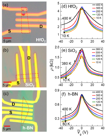
Experiments were performed with exfoliated graphene on 300 nm-SiO2/Si substrate blake2007making . Graphene samples were reliably identified as monolayers by means of Raman spectroscopy. ferrari2006raman ; graf2007spatially Figs. 1(a), (b) and (c) show optical images of graphene devices fabricated on HfO2, SiO2, and h-BN, respectively. For the preparation of graphene on HfO2, 30 nm-thick HfO2 was deposited on a SiO2/Si substrate by using atomic layer deposition (ALD) and graphene was transferred to the HfO2 film.jiao2008creation For the graphene device on h-BN, a 10 nm-thick flake of h-BN was first exfoliated on a SiO2/Si substrate, shown as green in Fig. 1(c), and then the graphene was transferred onto the h-BN flake. Electrodes were defined by using a conventional electron-beam lithography technique, and Pd(20 nm)/Au(30 nm) electrodes were deposited on top of the graphene. The temperature dependence of resistivity was studied between 10 and 400 K in a liquid helium system (Quantum Design PPMS).
Figs. 1(d), (e) and (f) display the resistivity as a function of gate voltage Ṽg at various fixed for graphene on HfO2, SiO2, and h-BN, respectively. The resistivity of graphene was larger on the HfO2 substrate for all applied gate voltages. Near the charge neutrality point (CNP), the resistivity of the graphene on HfO2 was five times larger than that of the graphene on h-BN. The mobility in graphene, estimated from positive gate voltages at K, was 3000, 5000 and 17000 cm2/Vs for HfO2, SiO2, and h-BN substrates, respectively. In the low- limit, the resistivity saturated at a temperature-independent value of for all three substrates, consistent with previous studies of graphene on SiO2.zou2010deposition ; chen2008intrinsic ; efetov2010controlling . At = 2 1012/cm2, we have of 1533, 540, 305 for HfO2, SiO2, and h-BN, respectively. The contact resistance of the Pd electrodes is about 10 to 30 .song2012determination ; watanabe2012low ; xia2011origins The residual resistivity mainly originates from electron scattering with static impurities and point defects. The h-BN substrate has an atomically smooth surface with less charge traps and dangling bonds,dean2010boron and in addition possesses a larger surface optical phonon energy of 101 meV, compared to 59 and 22 meV of SiO2 and HfO2, respectively. Therefore, the observed higher mobility and the smaller resistivity of the graphene on the h-BN substrate can be expected.
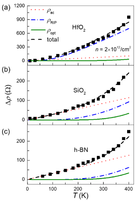
To investigate the role of surface optical phonons in more detail, we compare only the -dependent part of the resistivity, , for graphene samples prepared on the three different substrates. In Fig. 2, we plot , extracted from Fig. 1 for various at = 2 1012/cm2. Note is much larger for the graphene on HfO2.
We analyze and fit the -dependent resistivity by separating into three different contributions to the resistivity as follows.
| (1) |
() is the resistivity due to acoustic phonon scattering, and is linearly proportional to .hwang2008acoustic It is independent of carrier density and is given by
| (2) |
Here is Boltzmann’s constant, with and being the elementary charge and Planck constant, respectively. = 7.6 10-7 kg m-2 is the mass density of graphene. m/s is the Fermi velocity and m/s is the speed of sound. Red dotted lines in Fig. 2 indicate the contribution due to the acoustic phonon scattering and the slopes give the acoustic deformation potential = 303 eV, in good agreement with previous reports. hwang2008acoustic ; dean2010boron ; efetov2010controlling ; bolotin2008temperature shows a linear dependence at lower and becomes superlinear at higher , implying scattering with high-energy phonon modes. Note, whereas follows a linear behavior up to K for the graphene on h-BN (Fig. 2(c)), it deviates from the linear dependence already well below 100 K for the graphene on HfO2 (Fig. 2(a)).
The second term, (), expresses the resistivity contribution due to the scattering with remote interfacial phonons in the substrates, and can be written as chen2008intrinsic ; lin2013surface ; zou2010deposition
| (3) |
| Quantity (units) | HfO2zou2010deposition ; fischetti2001effective | SiO2fischetti2001effective ; fratini2008substrate | h-BNperebeinos2010inelastic ; geick1966normal |
|---|---|---|---|
| (meV) | 21 | 59 | 101 |
| (meV) | 54 | 155 | 196 |
| Scattering ratio | 0.96 | 6.83 | 2.17 |
Here and represent the energy of the two strongest surface optical phonon modes, with S being the ratio of coupling to the electrons. We used meV and 54 meV for HfO2, 59 and 155 meV for SiO2, and 101 and 196 meV for the h-BN substrate, respectively. In table I, the values of , and are summarized for the three different substrates.zou2010deposition ; perebeinos2010inelastic ; geick1966normal ; fischetti2001effective ; fratini2008substrate is a resistivity coefficient derived from fitting parameters and .chen2008intrinsic
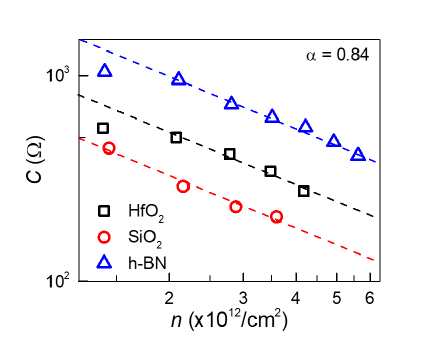
In Fig. 3, the resistivity coefficient is plotted as a function of the charge carrier density. The dashed lines represent fits with = 0.84. The resistivity coefficient decreases as carrier density increases due to the charge carrier screening effect.adam2007self ; siegel2013charge The difference in at the same carrier density is partly related to the difference in effective distance between the graphene and the substrate for each device. Following the approach of Ref. lin2013surface, , and using the relation, , we obtain 4.3, 1.4 and 1.3 Å for the graphene samples on HfO2, SiO2, and h-BN, respectively. Here, is the coupling parameter for the surface optical phonon mode and , with being the average dielectric permittivity of the air/graphene/substrate.lin2013surface Larger effective distance between the graphene and the HfO2 substrate is attributed to the roughness of the HfO2 after the ALD growth. An atomic force microscope (AFM) study shows much larger root-mean-square surface roughness of 10-14 Å for our HfO2 substrates, compared to 5 and 1-2 Å for SiO2, and h-BN, respectively.
The last term, () is the resistivity component due to electron scattering with the optical phonons of graphene. A phonon mode at K point, longitudinal (LO) and transverse optical (TO) phonon modes at point are considered. The A mode has an energy of 150 meV, and LO and TO modes have an energy of 200 meV. Owing to the relatively large energy, becomes important only above 300 K (Fig. 2). The resistivity induced by scattering between electrons and phonons can be expressed as follows.sohier2014phonon
| (4) |
is the relaxation time and depends on the optical phonon mode. is the equilibrium Fermi-Dirac distribution function. In the above equation, the density of states (DOS) of graphene and the relaxation time of each mode are substituted to calculate the resistivity component due to optical phonons.
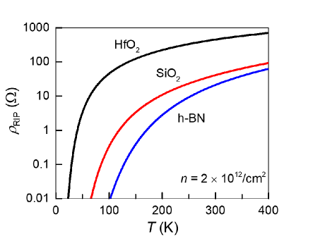
In Fig. 4, we plot as a function of temperature for = 2 1012/cm2 ( 170 meV). The resistivity arising from the surface phonon scattering is much larger for graphene on the HfO2 substrate. becomes larger than 10 above 60 K for HfO2, significantly at lower , compared to 200 and 250 K for SiO2 and h-BN, respectively. At K, it reaches 450 for graphene on the HfO2, whereas it remains below 20 for the h-BN substrate. Surface optical phonon energies of HfO2, SiO2 and h-BN are 21, 59 and 101 meV, respectively. The smaller surface phonon energy for HfO2 explains in general our results, yet larger Å for graphene on HfO2 leads to the underestimation of against values from other two substrates with Å. Note is inversely proportional to the effective graphene-substrate distance.
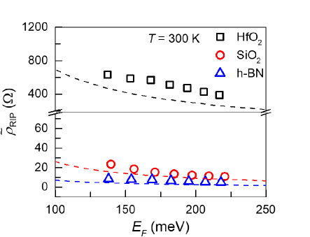
To compare our data with theoretical values from Ref. lin2013surface, , calculated for Å, we normalize to the effective graphene-substrate distance of 3.4 Å and display it in Fig. 5 as a function of the Fermi energy at 300 K. decreases as the Fermi energy increases because of the charge carrier screening effectadam2007self ; siegel2013charge . Our data are well matched to the theoretically calculated values, verifying the role of the remote interfacial phonons. Concerning the slight mismatch between our data and the theoretical values, we ignored in our discussion the out-of-plane (ZO) phonon mode in graphene. At ripples or bubbles, graphene floats locally and the out-of-plane ZO phonon mode ( meV) may play a role.morozov2008giant ; castro2010limits Also, we neglected the temperature dependence of contact resistance. A linear -dependence of contact resistance was reported for Pd-graphene contact.xia2011origins This can result in the overestimation of the acoustic deformation potential by eV in our previous discussion. On the other hand, the non-linear -dependent term for contact resistance is negligible.
In summary, we have studied the effect of surface optical phonons on the resistivity of graphene, prepared on three different substrates, HfO2, SiO2, and h-BN. For the h-BN substrate, with the larger surface optical phonon energy, the acoustic phonon scattering dominates and the resistivity shows a linear -dependence up to 200 K and then becomes superlinear. For the HfO2 substrate, with the lower surface optical phonon energy, the remote interfacial phonon scattering strongly dominates and results in much larger resistivity at room temperature. Our study suggests the use of an appropriate substrate can lead to a significant improvement in the charge transport of graphene.
Acknowledgements.
This paper was supported by Konkuk University in 2015.References
- (1) K. S. Novoselov, A. K. Geim, S. V. Morozov, D. Jiang, Y. Zhang, S. V. Dubonos, I. V. Grigorieva, and A. A. Firsov, Science 306, 666 (2004).
- (2) S. Morozov, K. Novoselov, M. Katsnelson, F. Schedin, D. Elias, J. A. Jaszczak, and A. Geim, Phys. Rev. Lett. 100, 016602 (2008).
- (3) K. I. Bolotin, K. Sikes, Z. Jiang, M. Klima, G. Fudenberg, J. Hone, P. Kim, and H. Stormer, Solid State Commun. 146, 351 (2008).
- (4) K. S. Novoselov, V. Fal, L. Colombo, P. Gellert, M. Schwab, and K. Kim, Nature (London) 490, 192 (2012).
- (5) H. Yang, J. Heo, S. Park, H. J. Song, D. H. Seo, K.-E. Byun, P. Kim, I. Yoo, H.-J. Chung, and K. Kim, Science 336, 1140 (2012).
- (6) J.-H. Chen, C. Jang, S. Xiao, M. Ishigami, and M. S. Fuhrer, Nat. Nanotechnol 3, 206 (2008).
- (7) I.-T. Lin and J.-M. Liu, Appl. Phys. Lett. 103, 081606 (2013).
- (8) P. Blake, E. Hill, A. C. Neto, K. Novoselove, D. Jiang, R. Yang, T. Booth, and A. Geim, Appl. Phys. Lett. 91, 063124 (2007).
- (9) A. Ferrari, J. Meyer, V. Scardaci, C. Casiraghi, M. Lazzeri, F. Mauri, S. Piscanec, D. Jiang, K. Novoselov, S. Roth, and A. Geim, Phys. Rev. Lett. 97, 187401 (2006).
- (10) D. Graf, F. Molitor, K. Ensslin, C. Stampfer, A. Jungen, C. Hierold, and L. Wirtz, Nano Lett. 7, 238 (2007).
- (11) L. Jiao, B. Fan, X. Xian, Z. Wu, J. Zhang, and Z. Liu, J. Am. Chem. Soc. 130, 12612 (2008).
- (12) K. Zou, X. Hong, D. Keefer, and J. Zhu, Phys. Rev. Lett. 105, 126601 (2010).
- (13) D. K. Efetov and P. Kim, Phys. Rev. Lett. 105, 256805 (2010).
- (14) S. M. Song, J. K. Park, O. J. Sul, and B. J. Cho, Nano Lett. 12, 3887 (2012).
- (15) E. Watanabe, A. Conwill, D. Tsuya, and Y. Koide, Diamond Relat. Mater. 24, 171 (2012).
- (16) F. Xia, V. Perebeinos, Y.-m. Lin, Y. Wu, and P. Avouris, Nat. Nanotechnol. 6, 179 (2011).
- (17) C. R. Dean, A. F. Young, I. Meric, C. Lee, L. Wang, S. Sorgenfrei, K. Watanabe, T. Taniguchi, P. Kim, K. Shepard, and J. Hone, Nat. Nanotechnol. 5, 722 (2010).
- (18) E. Hwang and S. D. Sarma, Phys. Rev. B 77, 115449 (2008).
- (19) K. Bolotin, K. Sikes, J. Hone, H. Stormer, and P. Kim, Phys. Rev. Lett. 101, 096802 (2008).
- (20) M. V. Fischetti, D. A. Neumayer, and E. A. Cartier, J. Appl. Phys. 90, 4587 (2001).
- (21) S. Fratini and F. Guinea, Phys. Rev. B 77, 195415 (2008).
- (22) V. Perebeinos and P. Avouris, Phys. Rev. B 81, 195442 (2010).
- (23) R. Geick, C. Perry, and G. Rupprecht, Phys. Rev. 146, 543 (1966).
- (24) S. Adam, E. Hwang, V. Galitski, and S. D. Sarma, Proc. Natl. Acad. Sci. U.S.A 104, 18392 (2007).
- (25) D. A. Siegel, W. Regan, A. V. Fedorov, A. Zettl, and A. Lanzara, Phys. Rev. Lett. 110, 146802 (2013).
- (26) T. Sohier, M. Calandra, C.-H. Park, N. Bonini, N. Marzari, and F. Mauri, Phys. Rev. B 90, 125414 (2014).
- (27) E. V. Castro, H. Ochoa, M. Katsnelson, R. Gorbachev, D. Elias, K. Novoselov, A. Geim, and F. Guinea, Phys. Rev. Lett. 105, 266601 (2010).