Large g factor in bilayer WS2 flakes
Abstract
The valley of transition metal dichalcogenides provides an additional platform to manipulate spin due to its unique selection rule. Normally, intralayer optical transitions in magnetic field show a Zeeman splitting with g factor of about . Here we report remarkable valley Zeeman effect exhibited by splitting of excitonic emission in a bilayer WS2, with a value of g factor as large as . The observed large g factor results from the interlayer recombination, as the conduction band and valence band are modified in opposite directions by magnetic field in different layers. The interlayer recombination is due to the defect induced inversion symmetry breaking, which is theoretically not accessible in ideal bilayer WS2 with inversion symmetry. Large g factor of interlayer emission offers potential benefits for future optical spin control and detection.
[figure]style=plain
Monolayer transition metal dichalcogenides (TMDs) have attracted considerable interests in their potentials for the next generation of nano-devices based on the valley pseudospin of electrons and holesXu et al. (2014). Valley-dependent optical polarization, arising from inversion symmetry breaking and strong spin-orbit coupling, provides a platform to manipulate spin information of photon, thus having prospects in quantum information processingGong et al. (2013); He et al. (2015); Srivastava et al. (2015). The study of the Zeeman splitting of the excitonic states plays an important role in investigating valleytronics, in which Landé g factor about has been obtained in monolayer WS2 both theoreticallyKoperski et al. (2019) and experimentallyKuhnert, Rahimi-Iman, and Heimbrodt (2017); Stier et al. (2016); Plechinger et al. (2016).
Recently, Giant pseudospsin g factors up to 38 have been observed in monolayer MoSe2 with controlling carrier concentration using a field transistor structure Wang, Mak, and Shan (2018); Back et al. (2017); Gustafsson et al. (2018). In the bilayer TMDs, however, there is an opportunity to increase the Zeeman splitting greatly by inducing interlayer emission. In natural TMDs materials, the adjacent layers are in reverse directions on the layer plane. The interlayer emission photons from adjacent layers are from combinations of electrons and holes in different valleys. Their corresponding valley orbital angular momenta are thus in opposite directions. When a magnetic field is applied, the energy levels of electrons and holes shift to opposite directions. Thus a larger g factor could be observed. Unfortunately, in ideal pristine bilayer TMDs, the interlayer emission is suppressed due to inversion symmetryGong et al. (2013); Zhu et al. (2014). Once inversion symmetry is broken, interlayer emission is no longer suppressed and a larger Zeeman splitting will appear. In fact, large g factors induced by symmetry breaking have been reported in heterostructures in MoSe2 /WSe2 Nagler et al. (2017) and in a bilayer MoTe2 Jiang et al. (2017). However, large g factor has not been reported in a bilayer WS2.
In this work, we report a large g factor in bilayer WS2 with numerous defects. The WS2 flakes were fabricated by exfoliating and the bilayer was confirmed by the thickness and the Raman characteristics. The Zeeman effect was investigated by the magneto-photoluminescence spectroscopy with a large g factor of about 16.5 observed at 30 K. We propose that the defect induced symmetry breaking leads to the interlayer emissions, resulting in the largely increased g factor.
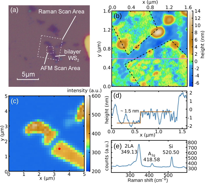
The WS2 flakes were mechanically exfoliated from bulk WS2 onto silicon substrates with 300-nm silica capping layer. To verify the number of layers, Atomic force microscopy (AFM) was performed with non-contact mode in air. The Raman spectrum was measured with a Raman microscope excited with a laser at nm. Microphotoluminescence (-PL) measurements were performed at 4.2 K and pumped with a -nm laser. Sample with WS2 flakes was placed on cryogenic confocal microscope system with high precision 3-dimensional piezo-driven motors. The PL spectra filtered with a nm long-pass filter were collected by spectrometer with a 300 g/mm grating. The sample was cooled down to K with liquid helium in the cryostat with a magnetic field from to T. An electric heater was used to heat the sample from to K.
Fig. 1(a) and (b) show the optical image and AFM image of the flake with a size of a few micrometers. The Raman intensity distribution of an out-of-plane motion mode (A1g peak) shown in Fig. 1(c) also reveals the shape of flakes, agreeing with optical and AFM images. According to the AFM scanning result (Fig. 1(b)), the material is not flat. The roughness of the flake surface implies the existence of defects. The result in Fig. 1(d) indicates that the height of thin part is about nm, which is the typical thickness of bilayer WS2Persson (2016). Although there are some contaminations in the AFM image outside the sample area (marked with dashed lines in Figure 1(b)), the bilayer height difference at the step edge is clear with considering both the AFM and Raman mode mapping. Meanwhile, according to the Raman spectrum shown in Fig. 1(e), the 2LA (second order longitude acoustic) peak at cm-1 and the A1g peak at cm-1 were observed. Comparing with the Raman results with an excitation laser at nmBerkdemir et al. (2013), the 2LA peak position around cm-1 is close to the peak position of trilayer and the much stronger intensity of 2LA than that of A1g implies monolayer. Nevertheless, the layer number should be less than three. Combining the AFM and Raman results, it can be confirmed that the region for the optical measurement is mainly a bilayer structure.
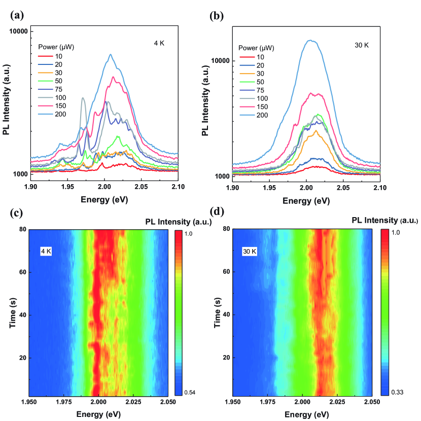
The measured PL spectra of our sample are unstable, in which the narrow peaks emerge and disappear randomly while a relatively stable broad peak always exists, as shown in Fig. 2. According to the peak wavelength, this wide peak is located in A exciton range, which is corresponding to the upper valence band in spin-orbit couplingXu et al. (2014). The peak is mainly from trions rather than neutral excitons at low temperature, according to the previous temperature-dependent PL spectraKato and Kaneko (2016); Plechinger et al. (2015). The neutral exciton peak is much weaker than trion and defect peaks at cryogenic temperaturePlechinger et al. (2015). As for the narrow peaks, not only the intensities but also the central wavelengths vary with time as shown in Fig. 2(c) and (d). The spectral fluctuation was also observed by other groups experimentallyBala et al. (2016); Chakraborty, Goodfellow, and Vamivakas (2016). Since these narrow peaks located at the red side of the trion, localized defect states are the most possible sourcesChakraborty, Goodfellow, and Vamivakas (2016). In addition to the existence of fluctuation, we also discover that the fluctuation is sensitive to temperature and pumping power. The spectrum becomes more stable with increasing pumping power as shown in Fig. 2(a) and (b). And the ratio of fluctuating peak intensity and the trion peak intensity decreases when temperature increases by comparing Fig. 2(c) at 4.2 K with Fig. 2(d) at 30 K.
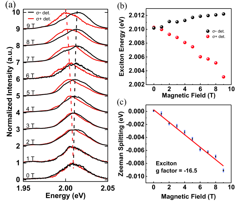
When a magnetic field perpendicular to the surface plane from T to T was applied, we observed a large Zeeman splitting of the wide peak as shown in Fig. 3(a). The sample was excited by linearly polarized laser to make two incident circularly polarized components equal. The polarization of PL was checked by a wave plate and a polarizer. The wave plate was controlled by a motor to measure two circularly polarized components of PL. The splitting and g factor were measured at different temperatures, ranging from K to K. Fig. 3 (b) and (c) show the fitted peak position and Zeeman splitting respectively, with the value of Landé g factor as large as at K. Additionally, there is a negative diamagnetic effect can be observed, which can be attributed to wavefunction expansion difference between initial and final states of the PL recombination for charged excitons Cao et al. (2015, 2016).
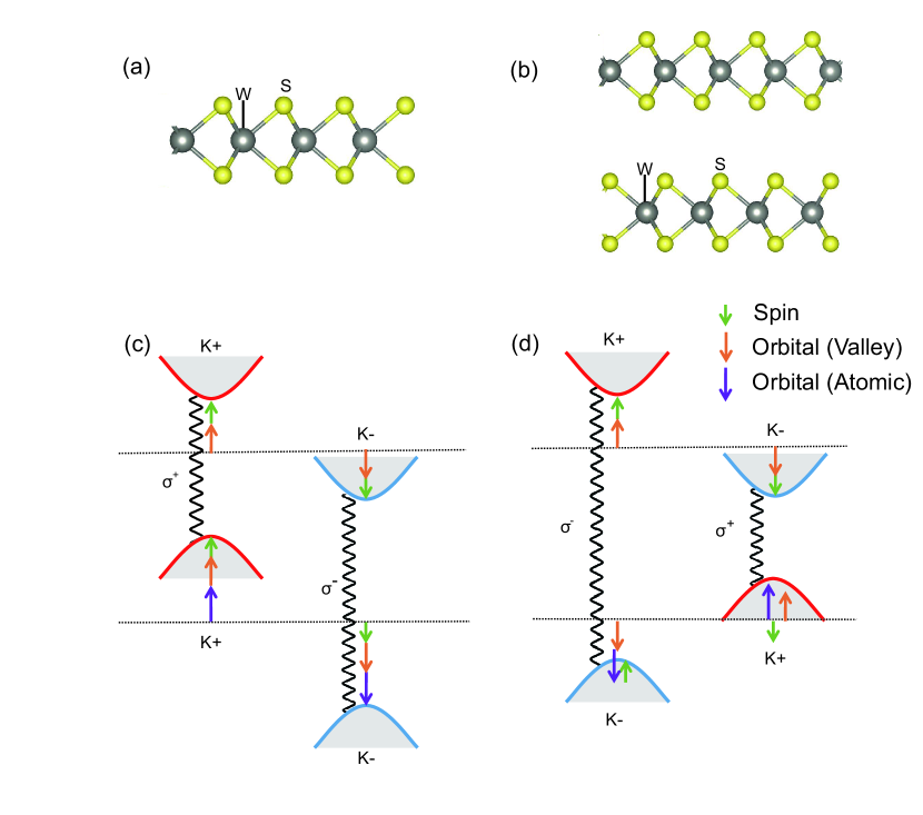
Figure 4 (a) and (b) show the crystal structure of single layer and bilayer WS2. To explain the observed large g factor, we attribute it to the enhanced interlayer recombination of bilayer WS2. The enhanced interlayer recombination could be due to the defect induced inversion symmetry breaking. Fig. 4 depicts the energy shift contributed by each angular momentum in monolayer and interlayer hopping respectively. Early modelGong et al. (2013) of theory gives the Hamiltonian as
| (1) |
Where the Pauli matrices are defined in basis of . The superscript and mean upper and lower layer respectively. The expressions describe the shapes of d orbit states of the transitional metal atom, which contribute to the states around valence band edge. is the energy dispersion, is the spin-valley coupling, is the valley index, is the interlayer hopping for holes, and denotes the spin. This model only considered spin contribution to the splitting, which is not sufficient to describe the large Zeeman splitting whose g factor is greater than . The orbital contribution to the Zeeman splitting should also be considered. A precise multiband model considering influences by other distant bands is more appropriate hereKormányos, Rakyta, and Burkard (2015); Wang et al. (2015); Rybkovskiy, Gerber, and Durnev (2017). The resulting g factor is given by,Nagler et al. (2017)
| (2) | ||||
Where indicates that the transition comes from the different or same valley, is the mass of free electron, is the effective mass of electron in conduction band at K point, and is the effective mass of hole in valence band at K point. In monolayer situation, take in , and the value of g factor is near . As for the interlayer emission, take in , and the value of g factor is much larger. There is an equivalent explanation of the model, which is easier to understand. Zeeman splitting is contributed by three factorsKoperski et al. (2017); Plechinger et al. (2016); Koperski et al. (2019), including spin, atomic orbital and valley orbital magnetic moment, as shown in Fig. 4(c) and (d). The spin contributes to the g factor. Because the shifts of conduction band and valence band are the same. The atomic orbital magnetic moment contributes . Because the conduction band is mainly , . The valence band is mainly , . The valley orbital magnetic moment contributes , which is related to Berry curvatureStier et al. (2016). Due to spin-orbit coupling, the conduction band also slightly splits into two bands. For WS2 materials, the splitting of spin state of upper conduction band is the same with that of the upper valence band, and the lower conduction band is corresponding to the lower valence bandKormányos et al. (2013); Liu et al. (2013).
According to the theoretical effective mass from Ref. Kormányos et al. (2015), the effective electron mass is for the upper conduction band and for the lower conduction band at K point. The effective hole mass is for the upper valence band and for the lower valence band. For A exciton, only the upper valence band should be considered. For , the spin state of upper conduction band is the same with the upper valence bandKormányos et al. (2013); Liu et al. (2013). Therefore, for monolayer situation, the predicted value of g factor should be around . But for interlayer situation, the predicted value of the g factor will increase to , which agrees well with our experimental results. The trend that interlayer g factor is much larger than intralayer g factor is consistent with different calculation methods, although the detailed effective masses might vary Kormányos et al. (2015); Ramasubramaniam (2012). If different effective masses are considered Ramasubramaniam (2012), the calculated g factors of interlayer emission could vary in the range of to . Nevertheless, the experimental result with value of g factor about verifies our assumption that the peak mainly comes from the interlayer emission.
It should be noted that defect related bound states may also attribute to the enhancement of g factorHe et al. (2015); Srivastava et al. (2015). In our case, it cannot be totally excluded in our measurement as the PL peak position is located at energy lower than the free excitons. However, normally the defected related bound states have much narrower linewidth of PL peaks, which can be identified in our sample at low temperature and are not stable as discussed above. Therefore, we believe the interlayer emission is dominated in our measurement for the broad peak at 30K, which corresponds well with our calculations as well.
In conclusion, a value of g factor as large as has been observed in a bilayer WS2 at K. The large g factor is due to interlayer emission, caused by inversion symmetry breaking induced by defects in the bilayer flakes. The existence of defects has been confirmed with AFM, Raman spectroscopy and fluctuating PL peak. The large g factor has been well explained with considering the effective masses in different valleys in bilayer situation. As the g factor increases, a larger energy difference between different spin states can be obtained with a small magnetic field. The results provide a great potential for spin initialization and detection, and a platform for valleytronics for on-chip optical quantum information devices.
Acknowledgements.
This work was supported by the National Natural Science Foundation of China under Grants No. 51761145104, No. 61675228, No. 11721404 and No. 11874419; the Strategic Priority Research Program, the Instrument Developing Project and the Interdisciplinary Innovation Team of the Chinese Academy of Sciences under Grants No. XDB07030200, No. XDB28000000 and No.YJKYYQ20180036.References
- Xu et al. (2014) X. D. Xu, W. Yao, D. Xiao, and T. F. Heinz, Nat. Phys. 10, 343 (2014).
- Gong et al. (2013) Z. R. Gong, G.-B. Liu, H. Y. Yu, D. Xiao, X. D. Cui, X. D. Xu, and W. Yao, Nat. Commun. 4, 2053 (2013).
- He et al. (2015) Y.-M. He, G. Clark, J. R. Schaibley, Y. He, M.-C. Chen, Y.-J. Wei, X. Ding, Q. Zhang, W. Yao, X. D. Xu, C.-Y. Lu, and J.-W. Pan, Nat. Nanotech. 10, 497 (2015).
- Srivastava et al. (2015) A. Srivastava, M. Sidler, A. V. Allain, D. S. Lembke, A. Kis, and A. Imamoǧlu, Nat. Nanotech. 10, 491 (2015).
- Koperski et al. (2019) M. Koperski, M. R. Molas, A. Arora, K. Nogajewski, M. Bartos, J. Wyzula, D. Vaclavkova, P. Kossacki, and M. Potemski, 2D Materials 6, 015001 (2019).
- Kuhnert, Rahimi-Iman, and Heimbrodt (2017) J. Kuhnert, A. Rahimi-Iman, and W. Heimbrodt, J. Phys.: Condens. Matter 29, 08LT02 (2017).
- Stier et al. (2016) A. V. Stier, K. M. McCreary, B. T. Jonker, J. Kono, and S. A. Crooker, Nat. Commun. 7, 10643 (2016).
- Plechinger et al. (2016) G. Plechinger, P. Nagler, A. Arora, A. Aguila, M. Ballottin, T. Frank, P. Steinleitner, M. Gmitra, J. Fabian, P. Christianen, R. Bratschitsch, C. Schüller, and T. Korn, Nano Lett. 16, 7899 (2016).
- Wang, Mak, and Shan (2018) Z. Wang, K. F. Mak, and J. Shan, Phys. Rev. Lett. 120, 066402 (2018).
- Back et al. (2017) P. Back, M. Sidler, O. Cotlet, A. Srivastava, N. Takemura, M. Kroner, and A. Imamoǧlu, Phys. Rev. Lett. 118, 237404 (2017).
- Gustafsson et al. (2018) M. V. Gustafsson, M. Yankowitz, C. Forsythe, D. Rhodes, K. Watanabe, T. Taniguchi, J. Hone, X. Zhu, and C. R. Dean, Nature Materials 17, 411 (2018).
- Zhu et al. (2014) B. R. Zhu, H. L. Zeng, J. F. Dai, Z. R. Gong, and X. D. Cui, PNAS 111, 11606 (2014).
- Nagler et al. (2017) P. Nagler, M. V. Ballottin, A. A. Mitioglu, F. Mooshammer, N. Paradiso, C. Strunk, R. Huber, A. Chernikov, P. C. M. Christianen, C. Schüller, and T. Korn, Nat. Commun. 8, 1551 (2017).
- Jiang et al. (2017) C. Y. Jiang, F. C. Liu, J. Cuadra, Z. M. Huang, K. Li, A. Srivastava, Z. Liu, and W.-B. Gao, Nat. Commun. 8, 802 (2017).
- Persson (2016) K. Persson, “Materials data on ws2 (sg:194),” https://materialsproject.org (2016).
- Berkdemir et al. (2013) A. Berkdemir, H. R. Gutiérrez, A. R. Botello-Méndez, N. P.-López, A. L. Elías, C.-I. Chia, B. Wang, V. H. Crespi, F. L.-Urías, J.-C. Charlier, H. Terrones, and M. Terrones, Sci. Rep. 3, 1755 (2013).
- Kato and Kaneko (2016) T. Kato and T. Kaneko, ACS Nano 10, 9687 (2016).
- Plechinger et al. (2015) G. Plechinger, P. Nagler, J. Kraus, N. Paradiso, C. Strunk, C. Schüller, and T. Korn, Phys. Stat. Sol. (RRL) 9, 457 (2015).
- Bala et al. (2016) L. Bala, E. M. Łacińska, K. Nogajewski, M. R. Molas, A. Wysmołek, and M. Potemski, Acta Phys. Pol. A 5, 1176 (2016).
- Chakraborty, Goodfellow, and Vamivakas (2016) C. Chakraborty, K. M. Goodfellow, and A. N. Vamivakas, Opt. Mater. Express 6, 2081 (2016).
- Cao et al. (2015) S. Cao, J. Tang, Y. Gao, Y. Sun, K. Qiu, Y. Zhao, M. He, J.-A. Shi, L. Gu, D. A. Williams, et al., Scientific reports 5, 8041 (2015).
- Cao et al. (2016) S. Cao, J. Tang, Y. Sun, K. Peng, Y. Gao, Y. Zhao, C. Qian, S. Sun, H. Ali, Y. Shao, et al., Nano Research 9, 306 (2016).
- Kormányos, Rakyta, and Burkard (2015) A. Kormányos, P. Rakyta, and G. Burkard, New Journal of Physics 17, 103006 (2015).
- Wang et al. (2015) G. Wang, L. Bouet, M. M. Glazov, T. A. E. L. Ivchenko, E. Palleau, X. Marie, and B. Urbaszek, 2D Materials 2, 034002 (2015).
- Rybkovskiy, Gerber, and Durnev (2017) D. V. Rybkovskiy, I. C. Gerber, and M. V. Durnev, Phys. Rev. B 95, 155406 (2017).
- Koperski et al. (2017) M. Koperski, M. R. Molas, A. Arora, K. Nogajewski, A. O. Slobodeniuk, C. Faugeras, and M. Potemski, Nanophotonics 6, 1289 (2017).
- Kormányos et al. (2013) A. Kormányos, V. Zólyomi, N. D. Drummond, P. Rakyta, G. Burkard, and V. I. Fal’ko, Phys. Rev. B 88, 045416 (2013).
- Liu et al. (2013) G.-B. Liu, W.-Y. Shan, Y. G. Yao, W. Yao, and D. Xiao, Phys. Rev. B 88, 085433 (2013).
- Kormányos et al. (2015) A. Kormányos, G. Burkard, M. Gmitra, J. Fabian, V. Zólyomi, N. D. Drummond, and V. Fal’ko, 2D Materials 2, 022001 (2015).
- Ramasubramaniam (2012) A. Ramasubramaniam, Phys. Rev. B 86, 115409 (2012).