A Theoretical Investigation of Charge Density Wave Instability in CuS
Abstract
The existence of a charge density wave (CDW) in transition metal dichalcogenide CuS has remained undetermined since its first experimental synthesis nearly 50 years ago. Despite conflicting experimental literature regarding its low temperature structure, there exists no theoretical study of the phonon properties and lattice stability of this material. By studying the first-principles electronic structure and phonon properties of CuS at various electronic temperatures, we identify temperature-sensitive soft phonon modes which unveil a previously unreported Kohn anomaly at approximately 100K. Variation of the electronic temperature shows the presence of two distinct phases, characterized at low temperature by a periodic charge modulation associated with the motion of the S dimers. Investigation of the Fermi surface presents a potential Fermi surface nesting vector related to the location of the Kohn anomaly and observed band splittings in the unfolded bandstructure. The combination of these results suggests a strong possibility of CDW order in CuS. Further study of CuS in monolayer form finds no evidence of a CDW phase, as the identified bulk periodic distortions cannot be realized in 2D. This behavior sets this material apart from other transition metal dichalcogenide materials, which exhibit a charge density wave phase down to the 2D limit. As CDW in TMDC materials is considered to compete with superconductivity, the lack of CDW in monolayer CuS suggests the possibility of enhanced superconductivity relative to other transition metal dichalcogenides. Overall, our work identifies CuS as a previously unrealized candidate to study interplay of superconductivity, CDW order, and dimensionality.
Transition metal dichalcogenides (TMDCs) like Ta, Nb(S,Se) have displayed interesting physics including charge density wave (CDW) formation and low temperature superconductivity Castro Neto (2001); Rossnagel (2011); Cudazzo et al. (2012); Frenzel et al. (2018); Basov et al. (2017); Keimer and Moore (2017); Cho et al. (2018). While bulk, layered TMDC structures can host CDW, recent studies have investigated the competition between CDW order and superconductivity, Chen et al. (2015); Chang et al. (2012); Cho et al. (2018) as well as the enhancement of superconducting T in monolayer TMDCs in relation to the suppression or lack of CDW order Frindt (1972); Yang et al. (2018); Wei et al. (2017); Navarro-Moratalla et al. (2016); Xi et al. (2015); Kang et al. (2011). Despite a lack of a unified understanding of the origins of CDW in TMDCs, thus far, studied examples have displayed similar CDW characteristics down to the 2D limit, possibly limiting T enhancement.
Though the superconducting behavior of TMDC CuS is well known Bither et al. (1968), there exists a long-standing debate about the existence of CDW order in this material Krill et al. (1976); Ueda et al. (2002). Initial studies of bulk susceptibility Bither et al. (1968); Gautier et al. (1974), nuclear magnetic resonance Gautier et al. (1974); Krill et al. (1976); Kontani et al. (2000), and specific heat Krill et al. (1976); Kontani et al. (2000) have presented evidence of a second order structural phase transition at 150K, hinting at the formation of a CDW structure. However, a more recent experiment rejected this possibility as a result of a contradictory Hall coefficient measurement Ueda et al. (2002), and this stance has been adopted by subsequent studies.
Throughout this experimental debate, theoretical study of CuS has remained extremely limited Bullett (1982); Temmerman et al. (1993); Kakihana et al. (2018). Presently, there are no reports of the phonon properties of CuS, which could provide critical insight regarding its structural phases. Theoretical studies of other CDW materials, including NbSe Calandra et al. (2009), TiSe Duong et al. (2015); Bianco et al. (2015) and TaSe Yan et al. (2015), have successfully captured CDW behavior and related phenomena through analysis of electronic-temperature dependent structural and electronic properties.
In this context, we present ab initio calculations of the electronic and phononic properties of CuS as a function of electronic temperatureBrown et al. (2016a); Shirodkar et al. (2018). We observe that the experimentally reported high-temperature structure Bither et al. (1968) exhibits instabilities and a Kohn anomaly in the phonon dispersion for calculations at low electronic temperature. By constructing and stabilizing a superstructure of CuS, we report for the first time the existence of a periodic manifestation of this material. We find that the transition to the distorted structure is governed by a twice-periodic displacement of the S dimers of CuS, resulting in a modulation of the charge density of the same periodicity. By evaluating the electronic structure of the low-temperature distorted structure, we observe the appearance of band splittings and identify a potential Fermi surface nesting vector associated with the Kohn anomaly. Subsequently, we investigate monolayer CuS Liu et al. (2018) and find no instabilities or any other hints of CDW formation, regardless of electronic temperature, possibly because it cannot host the dimer motions observed in the bulk structural distortion.
Together, our results strongly suggest CDW order in bulk CuS, and by identifying its origins, explain the absence of CDW in the 2D limit. We therefore present it as an exemplary platform to study the competition between superconductivity and CDW order, and in particular, the role dimensionality plays in these effects. We discuss the unique aspects of CDW formation relative to well-known TMDC materials, and further discuss pathways for enhancing superconductivity in both bulk and monolayer CuS.
In textbook 1D systems, the origin of CDW is conventionally analyzed in the Peierls instability picture Peierls (1930, 1956); Fröhlich (1954) where the system undergoes a periodic lattice distortion characterized by charge density modulation to form a symmetry-reduced state. This results in band splittings at the Fermi wavevector () related to a Fermi surface nesting vector , which connects multiple points on the Fermi surface and indicates the location of a Kohn anomaly in the phonon dispersion Kohn (1959). However, in higher dimensional systems, the analogy to the Peierls instability is not as straightforward Johannes and Mazin (2008) and Fermi surface nesting alone is generally not sufficient for understanding the origin of CDW formation. Other mechanisms include the excitonic insulator instability Bianco et al. (2015); Porer et al. (2014), Jahn-Teller effects Porer et al. (2014), momentum-dependent electron-phonon coupling Johannes and Mazin (2008); Zhu et al. (2015); Calandra et al. (2009) as well as a combination of these mechanisms.
Therefore, to investigate the occurrence of CDW in CuS, we begin by considering its structural stability. We start with the experimental pyrite (Pa3) structure measured at ambient temperatures Bither et al. (1968); Krill et al. (1976), with Cu atoms occupying fcc sites of the unit cell, and S dimers centered along cell edges. After structural relaxation, we perform density functional theory (DFT)Sundararaman et al. (2017) calculations with computational procedures previously introducedCiccarino et al. (2018); Narang et al. (2017); Brown et al. (2016b); Sundararaman et al. (2014). To describe CuS, we selected the ultrasoft RRKJ pseudopotentialsRappe et al. (1990); Dal Corso (2014) parameterized for the PBE exchange-correlation functionalPerdew et al. (1996). We also include a Hubbard U parameter (DFT+U) of eV, as determined from first principles linear response Cococcioni and de Gironcoli (2005). This relatively small is consistent with experimental studies which have found weak electronic correlation Ueda et al. (2002); Kakihana et al. (2018) in CuS, as we find the bands near the Fermi energy are mostly of Sulfur (as opposed to Copper ) character.
In order to probe temperature-dependent phenomena in CuS, we use the Fermi-Dirac smearing scheme to mimic an electronic temperature. All calculations where the smearing width or electronic temperature is not specified use a 0.001 Hartree smearing (equivalent to an electronic temperature of 315K). Finally, to compare the electronic structure of low- and high-symmetry structures, we apply a band unfolding technique. Here we determine the overlap of the supercell Bloch states with those of the primitive cell using a symmetry-averaged spectral function technique Tian et al. (2019), as outlined in Ref. 48.
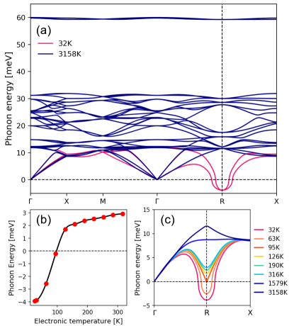
Initial calculations of the phonon dispersion of the experimental, high-temperature structure using low-temperature smearing reveal four soft phonon modes at the R point shown in Fig. 1(a). Upon varying the smearing parameter, we found these soft modes near this wavevector to be strongly sensitive to the electronic temperature, as shown in Fig. 1(b) and (c). We note the appearance of a discontinuity in the phonon dispersion (a Kohn anomaly) located at wavevector for an electronic temperature corresponding to approximately 100K.
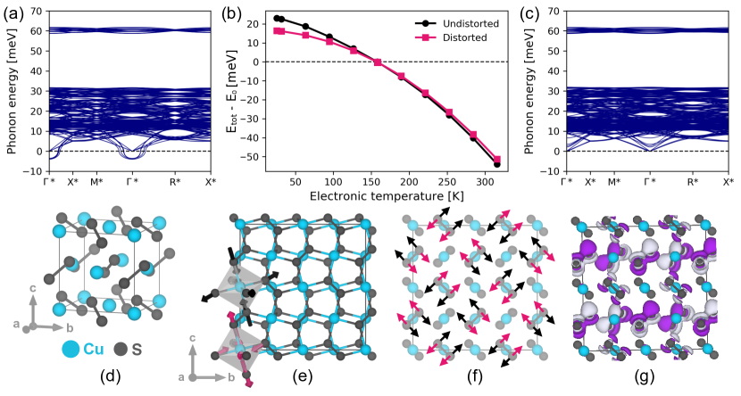
Motivated by past experimental work suggesting the existence of a superstructure in CuS at low temperatures Vanderschaeve and Escaig (1976), we sought to resolve the structural instability by using a supercell. The predicted phonon dispersion of the constructed supercell (depicted in Fig. 2(a)) reveals four negative phonon modes at an electronic temperature of 32K, consistent with the instabilities observed in the unit cell structure. We note the soft modes observed are at the point of the supercell, which is equivalent to R point in the original cell due to the corresponding change in the Brillouin zone of the supercell structure (see Fig. 1 in SI).
We identify the atomic displacements resulting from the four unstable phonon modes and observe each mode corresponds to periodic side-ways motions of S dimers, which cannot be captured in the single unit cell. These four modes collectively manifest themselves as an effective motion of the S dimers with a period of , twice the original unit cell lattice coefficient, as schematically shown in Fig. 2(f).
We perform energy minimization with respect to the ground state energy of the high-symmetry phase as a function of the magnitude of the eigendisplacements of each of these modes (for illustration of the individual modes and energy minimization, see Fig. 2 in SI). By applying this collective distortion to the constructed undistorted superstructure, we obtain a distorted structure with reduced symmetry, from (Pa3 to P-1) as shown in Fig. 2(e), and predict a stable phonon dispersion at low electronic temperatures (seen in Fig. 2(c)). These collective distortions lead to an alternating expansion and compression of Cu centered octahedra, as shown in Fig. 2(d), which could introduce a crystal field splitting of the orbital energy levels and may impact electron occupation and charge distribution near the Cu sites. By comparing the undistorted and distorted structures and calculating the difference in their charge densities, we identify a 2 periodic modulation of charge density, commensurate with the periodicity of the distorted structure, as shown in Fig. 2(g).
Additionally, we investigate the relative stability of the undistorted and distorted supercells (Fig.2(b)), and find that as we change electronic temperature of both structures, we see a crossover in the ground state energy at about 150K, a transition that would agree impressively well with experimental results Krill et al. (1976) and correspond to what was calculated in Fig. 1(b,c). When relaxed at higher electronic temperature, the distorted structure returns to the undistorted structure, indicating the process can be reversed.
The combination of the observed Kohn anomaly, periodic lattice distortion, periodic charge density modulation, and temperature-dependent phase crossover are all indicative of the presence of CDW in bulk CuS. Our results therefore capture, for the first time in a theoretical study, a stable low temperature distorted phase of CuS exhibiting strong indicators of CDW ordering.
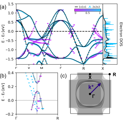
To understand the electronic origins of the potential CDW phase, we investigate the corresponding changes in the electronic structure. By using a band unfolding technique, we compare the effective band structure of the distorted supercell with that of the undistorted structure, seen in Fig. 3(a). We observe that the distortion results in multiple band splittings and formation of small gaps at multiple points along the band path. The locations of these gaps tend to occur halfway between high symmetry points (e.g., and R, R and X) and slightly above the Fermi energy level, in contrast to gap openings observed at in other CDW materials Yang et al. (2018); Singh et al. (2017); Rossnagel (2011).
We particularly focus on the splitting at approximately 0.2 eV above the Fermi level (Fig. 3(b)), which is centered at a wavevector , half that of the vector where the Kohn anomaly was observed in the undistorted structure). We find that this wavevector, when overlaid with the Fermi surface shown in Fig. 3(c), points to a saddle point in the surface, and that twice this vector () connects such saddle points diagonally across the Fermi surface. In the conventional 1D model of CDW formation Fröhlich (1954); Peierls (1956), the Peierls instability results in band gap formation at and a Kohn anomaly located at . This appears to be the case in CuS, indicating that Fermi surface nesting could be responsible for CDW formation in this material, contrary what occurs in NbSe Weber et al. (2011); Johannes and Mazin (2008) and TaSe Johannes and Mazin (2008) where no effective nesting exists at the CDW wavevector.
Additionally, we find that CuS shows weak electronic correlation Sachdev and Georges (1995) due to the dominance of sulfur rather than Cu orbitals at the Fermi level, while the gaps are energetically away from the Fermi level. This suggests a Mott-Hubbard-type metal-insulator transition Johnston et al. (2014) cannot provide a significant contribution to CDW formation. We also note that the splitting of the orbital energy level as a result of compression and expansion of alternating Cu site octahedral environments, which would account for the change in bandstructure approximately 0.5 eV below the Fermi energy level between the X and M points. This is supported by analyzing the relative contribution of and characteristics to the density of states (see SI Fig. 3). The resulting occupation shifts in the orbitals are due to shifts in shells, which, because they are energetically positioned below the Fermi level, cannot strongly contribute to the understanding of the observed gaps located slightly above the Fermi energy.
Despite the hints at Fermi surface nesting related CDW and band gap formation in bulk CuS, we note that there are a number of possible mechanisms which could result in a gap opening Dessau et al. (1998) and CDW formation, including the Jahn-Teller effect Porer et al. (2014) and the electron-phonon interaction Wijayaratne et al. (2017); Weber et al. (2011), which require further study in CuS.
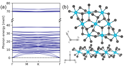
Beyond our investigation of bulk CuS, we extend our work to include its monolayer, which is formed as a quasi-layered hexagonal structure along the close-packed (111) plane as illustrated in Fig. 4(b). We predict a stable phonon dispersion for this structure, as shown in Fig. 4(a). Neither a Kohn anomaly nor soft phonon modes are observed for the same electronic temperature range, indicating the absence of CDW order in the monolayer limit. This finding agrees with experimental results which saw no CDW signature in thin film CuS on a SrTiO substrate Liu et al. (2018).
This prediction raises questions as to why CDW order in bulk does not persist to the monolayer, in contrast to other layered TMDC materials Ryu et al. (2018); Sakabe et al. (2017); Singh et al. (2017); Calandra et al. (2009). Understanding the difference between these two structures opens up a new avenue to understand CDW formation in the bulk structure. We note that the monolayer cannot capture the side-ways S dimer motions seen in our calculated bulk distorted superstructure, and as a result, we find the stability of the monolayer supports our finding and predicted origin of the potential CDW behavior in bulk CuS. However, a deeper understanding of the difference in bulk and monolayer structures prompts further study, particularly in attempts to increase the superconducting critical temperature in monolayer CuS. Therefore, we highlight the importance of this system as an ideal platform to study the coexistence of CDW order and superconductivity.
While the structural phase diagram of CuS has remained a debate for years, we uncover critical information regarding its ability to manifest a CDW structure through theoretical and computational methods. We predict temperature-sensitive soft phonon modes that appear at low electronic temperatures in the experimentally reported structure of CuS, corresponding to a Kohn anomaly at the R point for an electronic temperature of approximately 100K. We then realize the existence of a stable distorted phase with a 2 periodic lattice distortion and corresponding charge modulation at low electronic temperature. From this theoretical calculation, we establish a potential CDW transition and predict a crossover between the low and high symmetry structures at approximately 150K, in impressive agreement with what is reported in experiment. To further probe the electronic origins of the newly identified CDW structure, we observe a prominent band splitting near the Fermi energy at a wavevector half that of where the original instability occurred, similar to what is expected in the 1D perspective of CDW formation. Finally, we predict a stable monolayer with no CDW order signatures observed, in agreement with recent experiments, and note the potential difference in available dimer distortions as a possible reason for the lack of CDW in the monolayer.
Through this investigation of the phonon properties and electronic character of CuS, we report strong evidence of CDW in bulk CuS, suggesting Fermi surface nesting as an explanation for its occurrence. Additionally, because CuS lacks strong electronic correlations and simultaneously exhibits superconductivity, we identify this system as a promising platform to study the competition of superconductivity and CDW. In future work, we envision experimental studies of CDW order in bulk CuS (and absence thereof in monolayer) through angle resolved photoemission spectroscopy (ARPES and tr-ARPES), and low temperature scanning transmission electron microscopy (STEM).
Acknowledgements
The authors acknowledge funding from the Defense Advanced Research Projects Agency (DARPA) Defense Sciences Office (DSO) Driven and Nonequilibrium Quantum Systems program and the ONR grant on High-Tc Superconductivity at Oxide-Chalcogenide Interfaces (N00014-18-1-2691). This research used resources of the National Energy Research Scientific Computing Center, a DOE Office of Science User Facility supported by the Office of Science of the U.S. Department of Energy under Contract No. DE-AC02-05CH11231, as well as resources at the Research Computing Group at Harvard University. JC recognizes the support of the DOE Computational Science Graduate Fellowship (CSGF) under grant DE-FG02-97ER25308.
References
- Castro Neto (2001) A. H. Castro Neto, Physical Review Letters 86, 4382 (2001).
- Rossnagel (2011) K. Rossnagel, Journal of Physics: Condensed Matter 23, 213001 (2011).
- Cudazzo et al. (2012) P. Cudazzo, M. Gatti, and A. Rubio, Physical Review B 86, 075121 (2012).
- Frenzel et al. (2018) A. J. Frenzel, A. S. McLeod, D. Z.-R. Wang, Y. Liu, W. Lu, G. Ni, A. W. Tsen, Y. Sun, A. N. Pasupathy, and D. N. Basov, Phys. Rev. B 97, 035111 (2018).
- Basov et al. (2017) D. N. Basov, R. D. Averitt, and D. Hsieh, Nat. Mater. 16, 1077 (2017).
- Keimer and Moore (2017) B. Keimer and J. Moore, Nature Physics 13, 1045 (2017).
- Cho et al. (2018) K. Cho, M. Kończykowski, S. Teknowijoyo, M. A. Tanatar, J. Guss, P. B. Gartin, J. M. Wilde, A. Kreyssig, R. J. McQueeney, A. I. Goldman, V. Mishra, P. J. Hirschfeld, and R. Prozorov, Nature Communications 9, 2796 (2018).
- Chen et al. (2015) P. Chen, Y.-H. Chan, X.-Y. Fang, Y. Zhang, M. Y. Chou, S.-K. Mo, Z. Hussain, A.-V. Fedorov, and T.-C. Chiang, Nature Communications 6, 8943 (2015).
- Chang et al. (2012) J. Chang, E. Blackburn, A. T. Holmes, N. B. Christensen, J. Larsen, J. Mesot, R. Liang, D. A. Bonn, W. N. Hardy, A. Watenphul, M. v. Zimmermann, E. M. Forgan, and S. M. Hayden, Nature Physics 8, 871 (2012).
- Frindt (1972) R. F. Frindt, Phys. Rev. Lett. 28, 299 (1972).
- Yang et al. (2018) Y. Yang, S. Fang, V. Fatemi, J. Ruhman, E. Navarro-Moratalla, K. Watanabe, T. Taniguchi, E. Kaxiras, and P. Jarillo-Herrero, Physical Review B 98 (2018), 10.1103/PhysRevB.98.035203.
- Wei et al. (2017) M. J. Wei, W. J. Lu, R. C. Xiao, H. Y. Lv, P. Tong, W. H. Song, and Y. P. Sun, Physical Review B 96, 165404 (2017).
- Navarro-Moratalla et al. (2016) E. Navarro-Moratalla, J. O. Island, S. Mañas-Valero, E. Pinilla-Cienfuegos, A. Castellanos-Gomez, J. Quereda, G. Rubio-Bollinger, L. Chirolli, J. A. Silva-Guillén, N. Agraït, et al., Nature communications 7, 11043 (2016).
- Xi et al. (2015) X. Xi, L. Zhao, Z. Wang, H. Berger, L. Forró, J. Shan, and K. F. Mak, Nature nanotechnology 10, 765 (2015).
- Kang et al. (2011) L. Kang, B. Jin, X. Liu, X. Jia, J. Chen, Z. Ji, W. Xu, P. Wu, S. Mi, A. Pimenov, et al., Journal of Applied Physics 109, 033908 (2011).
- Bither et al. (1968) T. A. Bither, R. J. Bouchard, W. H. Cloud, P. C. Donohue, and W. J. Siemons, Inorganic Chemistry 7, 2208 (1968).
- Krill et al. (1976) G. Krill, P. Panissod, M. F. Lapierre, F. Gautier, C. Robert, and M. N. Eddine, Journal of Physics C: Solid State Physics 9, 1521 (1976).
- Ueda et al. (2002) H. Ueda, M. Nohara, K. Kitazawa, H. Takagi, A. Fujimori, T. Mizokawa, and T. Yagi, Physical Review B 65 (2002), 10.1103/PhysRevB.65.155104.
- Gautier et al. (1974) F. Gautier, G. Krill, P. Panissod, and C. Robert, Journal of Physics C: Solid State Physics 7, L170 (1974).
- Kontani et al. (2000) M. Kontani, T. Tutui, T. Moriwaka, and T. Mizukoshi, Physica B: Condensed Matter 284-288, 675 (2000).
- Bullett (1982) D. W. Bullett, Journal of Physics C: Solid State Physics 15, 6163 (1982).
- Temmerman et al. (1993) W. Temmerman, P. Durham, and D. Vaughan, Physics and Chemistry of Minerals 20 (1993), 10.1007/BF00208138.
- Kakihana et al. (2018) M. Kakihana, T. D. Matsuda, R. Higashinaka, Y. Aoki, A. Nakamura, D. Aoki, H. Harima, M. Hedo, T. Nakama, and Y. Ōnuki, Journal of the Physical Society of Japan 88, 014702 (2018).
- Calandra et al. (2009) M. Calandra, I. I. Mazin, and F. Mauri, Physical Review B 80 (2009), 10.1103/PhysRevB.80.241108.
- Duong et al. (2015) D. L. Duong, M. Burghard, and J. C. Schön, Physical Review B 92 (2015), 10.1103/PhysRevB.92.245131.
- Bianco et al. (2015) R. Bianco, M. Calandra, and F. Mauri, Physical Review B 92, 094107 (2015).
- Yan et al. (2015) J.-A. Yan, M. A. D. Cruz, B. Cook, and K. Varga, Scientific Reports 5, 16646 (2015).
- Brown et al. (2016a) A. M. Brown, R. Sundararaman, P. Narang, W. A. Goddard, and H. A. Atwater, Phys. Rev. B 94, 075120 (2016a).
- Shirodkar et al. (2018) S. N. Shirodkar, M. Mattheakis, P. Cazeaux, P. Narang, M. Soljačić, and E. Kaxiras, Phys. Rev. B 97, 195435 (2018).
- Liu et al. (2018) C. Liu, H. Yang, C.-L. Song, W. Li, K. He, X.-C. Ma, L. Wang, and Q.-K. Xue, Chinese Physics Letters 35, 027303 (2018).
- Peierls (1930) R. Peierls, Annalen der Physik 396, 121 (1930).
- Peierls (1956) R. E. Peierls, Quantum theory of solids (Clarendon Pr., 1956).
- Fröhlich (1954) H. Fröhlich, Proceedings of the Royal Society of London. Series A. Mathematical and Physical Sciences 223, 296 (1954).
- Kohn (1959) W. Kohn, Physical Review Letters 2, 393 (1959).
- Johannes and Mazin (2008) M. D. Johannes and I. I. Mazin, Physical Review B 77 (2008), 10.1103/PhysRevB.77.165135.
- Porer et al. (2014) M. Porer, U. Leierseder, J.-M. Ménard, H. Dachraoui, L. Mouchliadis, I. E. Perakis, U. Heinzmann, J. Demsar, K. Rossnagel, and R. Huber, Nature Materials 13 (2014), 10.1038/nmat4042.
- Zhu et al. (2015) X. Zhu, Y. Cao, J. Zhang, E. W. Plummer, and J. Guo, Proceedings of the National Academy of Sciences 112, 2367 (2015).
- Sundararaman et al. (2017) R. Sundararaman, K. Letchworth-Weaver, K. A. Schwarz, D. Gunceler, O. Yalcin, and T. Arias, SoftwareX 6, 278 (2017).
- Ciccarino et al. (2018) C. J. Ciccarino, T. Christensen, R. Sundararaman, and P. Narang, Nano Letters (2018), 10.1021/acs.nanolett.8b02300.
- Narang et al. (2017) P. Narang, L. Zhao, S. Claybrook, and R. Sundararaman, Adv. Opt. Mater. 5, 1600914 (2017).
- Brown et al. (2016b) A. M. Brown, R. Sundararaman, P. Narang, W. A. Goddard, and H. A. Atwater, ACS Nano 10, 957 (2016b).
- Sundararaman et al. (2014) R. Sundararaman, P. Narang, A. S. Jermyn, W. A. Goddard III, and H. A. Atwater, Nat. Commun. 5 (2014), 10.1038/ncomms6788.
- Rappe et al. (1990) A. M. Rappe, K. M. Rabe, E. Kaxiras, and J. D. Joannopoulos, Physical Review B 41, 1227 (1990).
- Dal Corso (2014) A. Dal Corso, Computational Materials Science 95, 337 (2014).
- Perdew et al. (1996) J. P. Perdew, K. Burke, and M. Ernzerhof, Phys. Rev. Lett. 77, 3865 (1996).
- Cococcioni and de Gironcoli (2005) M. Cococcioni and S. de Gironcoli, Phys. Rev. B 71, 035105 (2005).
- Tian et al. (2019) X. Tian, D. S. Kim, S. Yang, C. J. Ciccarino, Y. Gong, Y. Yang, Y. Yang, B. Duschatko, Y. Yuan, P. M. Ajayan, J.-C. Idrobo, P. Narang, and J. Miao, arXiv:1901.00633 [cond-mat] (2019), arXiv: 1901.00633.
- Medeiros et al. (2014) P. V. C. Medeiros, S. Stafström, and J. Björk, Physical Review B 89 (2014), 10.1103/PhysRevB.89.041407.
- Vanderschaeve and Escaig (1976) G. Vanderschaeve and B. Escaig, Materials Research Bulletin 11 (1976), 10.1016/0025-5408(76)90228-2.
- Singh et al. (2017) B. Singh, C.-H. Hsu, W.-F. Tsai, V. M. Pereira, and H. Lin, Physical Review B 95 (2017), 10.1103/PhysRevB.95.245136, arXiv: 1702.08329.
- Weber et al. (2011) F. Weber, S. Rosenkranz, J.-P. Castellan, R. Osborn, R. Hott, R. Heid, K.-P. Bohnen, T. Egami, A. H. Said, and D. Reznik, Physical Review Letters 107 (2011), 10.1103/PhysRevLett.107.107403.
- Sachdev and Georges (1995) S. Sachdev and A. Georges, Physical Review B 52, 9520 (1995).
- Johnston et al. (2014) S. Johnston, A. Mukherjee, I. Elfimov, M. Berciu, and G. A. Sawatzky, Physical Review Letters 112, 106404 (2014).
- Dessau et al. (1998) D. S. Dessau, T. Saitoh, C.-H. Park, Z.-X. Shen, P. Villella, N. Hamada, Y. Moritomo, and Y. Tokura, Physical Review Letters 81 (1998), 10.1103/PhysRevLett.81.192.
- Wijayaratne et al. (2017) K. Wijayaratne, J. Zhao, C. Malliakas, D. Young Chung, M. G. Kanatzidis, and U. Chatterjee, Journal of Materials Chemistry C 5, 11310 (2017).
- Ryu et al. (2018) H. Ryu, Y. Chen, H. Kim, H.-Z. Tsai, S. Tang, J. Jiang, F. Liou, S. Kahn, C. Jia, A. A. Omrani, J. H. Shim, Z. Hussain, Z.-X. Shen, K. Kim, B. I. Min, C. Hwang, M. F. Crommie, and S.-K. Mo, Nano Letters 18, 689 (2018).
- Sakabe et al. (2017) D. Sakabe, Z. Liu, K. Suenaga, K. Nakatsugawa, and S. Tanda, npj Quantum Materials 2, 22 (2017).