Electronic states of (InGa)(AsSb)/GaAs/GaP quantum dots
Abstract
Detailed theoretical studies of the electronic structure of (InGa)(AsSb)/GaAs/GaP quantum dots are presented. This system is unique since it exhibits concurrently direct and indirect transitions both in real and momentum space and is attractive for applications in quantum information technology, showing advantages as compared to the widely studied (In,Ga)As/GaAs dots. We proceed from the inspection of the confinement potentials for and conduction and valence bands, through the formulation of calculations for -indirect transitions, up to the excitonic structure of -transitions. Throughout this process we compare the results obtained for dots on both GaP and GaAs substrates, enabling us to make a direct comparison to the (In,Ga)As/GaAs quantum dot system. We also discuss the realization of quantum gates.
pacs:
78.67.Hc, 73.21.La, 85.35.Be, 77.65.LyI Introduction
Monolithic integration of III-V compounds with Si-technology is one of the key challenges of future photonics Liang and Bowers (2010). The problems caused by the large lattice mismatch between Si and typical emitter materials based on GaAs or InP substrates can be avoided to a large extent by employing a pseudomorphic approach, i.e. growing almost lattice matched compounds on Si. The III-V binary compound with the lattice constant closest to Si is GaP (0.37% lattice mismatch at 300K). GaP is an indirect semiconductor, and thus not seen as a useful laser material. It might serve however as a matrix for more appropriate material combinations. The initially obvious choice of employing InGaP as active material fails due to the borderline type-I/II nature of the bandoffset to GaP Hatami et al. (2003). (In,Ga)As/GaP, by contrast, features a type-I lineup and triggered a fair amount of research, both experimental and theoretical in nature Leon et al. (1998); Guo et al. (2009); Shamirzaev et al. (2010); Umeno et al. (2010); Fuchi et al. (2004); Nguyen Thanh et al. (2011); Rivoire et al. (2012). The main issue with this material combination is the large lattice mismatch and the resulting large strain in the (In,Ga)As active material, possibly leading to direct - indirect crossover of the ground state transition. Fukami et al. Fukami et al. (2011) were the first to evaluate the necessary fraction of In for a direct electron-hole ground state transition using model-solid theory for (InGa)(AsN)/GaP. Further theoretical insight was provided by the work of Robert et al. Robert et al. (2012, 2014, 2016) who first employed a mixed / tight-binding simulations, predicting a direct-indirect crossover at about 30% In-content for larger (In,Ga)As/GaP quantum dots (QDs). For smaller QDs they predicted an even larger In content for the direct transition in reciprocal space.
 |
In the present work we take the next step and assess the role of additional antimony incorporation, leading to In1-xGaxAsySb1-y/GaP QDs based on the experimental works of Sala et al. Sala et al. (2016); Sala (2018); Sala et al. (2018). Not only will we look at its suitability as optoelectronic material Arx (a) but also - as discussed by Sala et al. Sala (2018); Sala et al. (2018) - as material for QD-Flash memories.
The QD-Flash memory concept was suggested and developed by Bimberg et al. over a period of 20 years following the first studies by Kapteyn at al. on electron escape mechanism from InAs QDs using the deep level transient spectroscopy (DLTS) Kapteyn et al. (1999); Marent et al. (2011); Bonato et al. (2016); Bim . The concept, protected by 16 patents worldwide, attempts to combine the best of both memory worlds, the Dynamic Random Access Memories (DRAM) and the Flash worlds leading to a universal memory, strongly simplifying computer architecture. Fast read-write-erase operations, as fast or faster than those in current DRAM, shall be combined with non-volatility of information for more than 10 years in the same device. Presently most promising storage elements are of type-II QDs storing solely holes. GaSb QDs embedded in GaP show hole retention times of 4 days and the limit of 10 years is predicted to be crossed by varying the structures to (In,Ga)Sb QDs embedded in (Al,Ga)P.
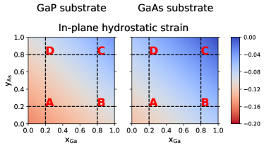
The secret for successful growth of such In1-xGaxAsySb1-y/GaP QDs by MOCVD constitutes a 5 ML GaAs interlayer (IL) on top of the GaP matrix material, thus, enabling QD formation Sala et al. (2016); Sala (2018), which will be carefully considered in the following simulations. The choice of GaAs layer is evident from Fig. 1 where we compare the effects of the GaP and more conventional GaAs substrates on hydrostatic strain in hypothetical bulk lattice-matched In1-xGaxAsySb1-y alloy. Note that Fig. 1 highlights also the labelling convention used in this work in order to avoid confusion: the Ga content in In1-xGaxAsySb1-y is marked as while that for As is .
II General remarks and outline
In our system, compared to e.g. (In,Ga)As/GaAs QDs, the -indirect electron states attain lower energy than the ones. This is a result of the large compressive strain in QDs occurring due to GaP substrate. Moreover, the eight- (six-) fold symmetry of L (X) bulk Bloch waves translates into four- (three-) L (X) envelope functions for quasiparticles in QDs, since each state is shared by two neighbouring Brillouin zones. We denote the resulting envelope wavefunctions L[110], L, L, and L (X[100], X[010], and X[001]). The degeneracy of envelopes for L[110], L, L, and L, or X[100], X[010], and X[001] bands is lifted in real dots due to structural imperfections (e.g. shape, composition) or by external perturbations (e.g. electric, magnetic, or strain fields) and we thus distinguish between these bands in the following, and study also the effects of degeneracy lifting. We carefully choose three exemplary points A, B, C, and D as seen in Fig. 1 and Tab. 1, that exhibit certain specific properties of our system, which will be discussed further in the the body of the paper.
| A | = 0.2; = 0.2 |
|---|---|
| B | = 0.8; = 0.2 |
| C | = 0.8; = 0.8 |
| D | = 0.2; = 0.8 |
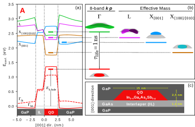
The paper is organized as follows: first we introduce our method of calculation. Single-particle states are calculated as a combination of one-band (for L- and X-point states) and eight-band approximation (for point states) {see top inset of Fig. 2 (b) and Fig. 3}. Owing to the very large lattice-mismatch between GaP and the QD-material, a method for the calculation of the inhomogeneous strain and its impact on the local bandedges is introduced, together with the effect of piezoelectricity. Our methods for accounting Coulomb interaction and calculation of optical properties are introduced thereafter.
Next, we continue with the analysis of the arising confinement potentials {Fig. 2 (a)} and analyze the electron and hole probability densities and eigen energies, respectively {Fig. 2 (b)}. Based on these results, we then inspect the electron-hole Coulomb integrals for -point states and derive information on type-I/II behavior. Then we discuss the localization energies of holes in our dots, which are relevant for the QD-flash memory concepts. We continue by studying the emission properties and the fine-structure of those excitons consisting of -electrons and holes. Finally, we present an application of In1-xGaxAsySb1-y/GaAs/GaP QD system as a possible realization of quantum gate and briefly discuss its properties.
 |
III Method of calculation
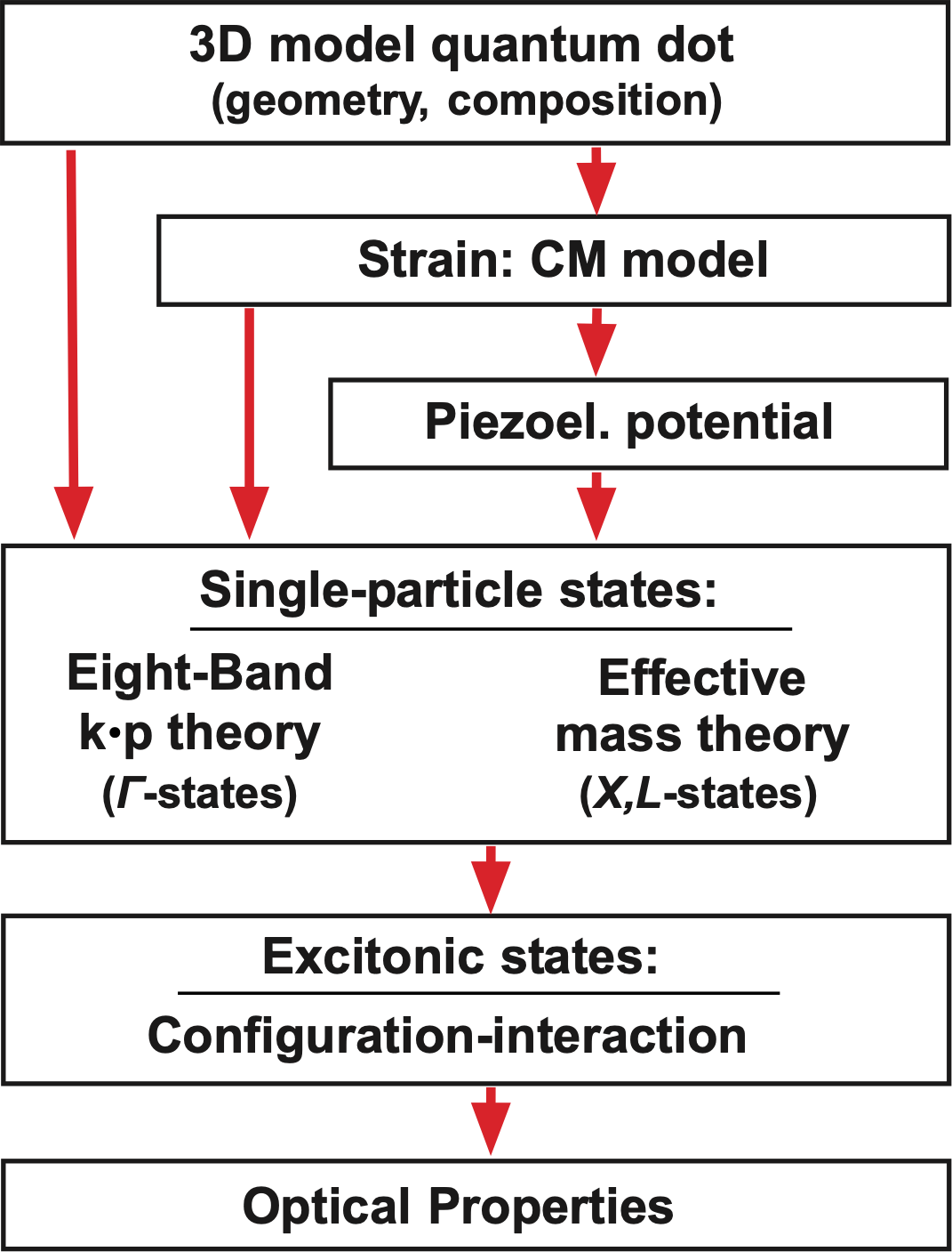 |
Figure 3 shows an outline of the modelling procedure employed in this paper. It starts with an implementation of the 3D QD model structure (size, shape, chemical composition), and carries on with the calculation of strain and piezoelectricity. The resulting strain and polarization fields then either enter the eight-band Hamiltonian for states located around the Brillouin-zone-center (-point), or the effective-mass Hamiltonian for those emerging off-center such as L- and X-point states. Solution of the resulting Schrödinger equations yields electron and hole single-particle states both at the - as well at X- and L-points. Coulomb interaction is accounted for by employing the configuration interaction (CI) method including dipole-dipole interaction. Finally, optical properties such as absorption spectra, capture cross sections, or lifetimes can be calculated.
III.1 Choice of model structure
The morphology of our model QD is related to the works of Stracke and Sala Stracke et al. (2014); Sala et al. (2016); Sala (2018); Sala et al. (2018): The whole structure is grown on GaP substrate with an IL between QD and substrate made of 5 ML GaAs {see Fig. 2 (c)}. Generally, the IL is of critical importance to enable the QD formation, as discovered by Stracke and coworkers for the In1-xGaxAs/GaAs/GaP QDs Stracke et al. (2012, 2014). There, the IL thickness used was around 2-3 ML, which remarkably affected the GaP surface reconstruction and diffusion, eventually enabling the QD formation. Similarly, for In1-xGaxAsySb1-y/GaAs/GaP QDs, the GaAs IL is used to enable the QD growth, but its thickness is of about 5ML Sala et al. (2016); Sala (2018). Here, it’s very likely that an intermixing via As-for-Sb exchange between the GaAs IL and the Sb of the QDs takes place, such that part of the IL becomes part of the QDs. Such process may lower the strain between QDs and GaP, where nominally the lattice mismatch was very high (nominally of 13 between In0.5Ga0.5Sb/GaP) for enabling an usual Stranski-Krastanov QD growth. Therefore, such intermixing may have lowered the high mismatch, thus enabling the QD formation Sala et al. (2016); Sala (2018); Sala et al. (2018), similarly observed also in Abramkin et al. Abramkin et al. (2014) for GaSb/GaP QDs. Note, that we do not consider the described intermixing of Sb to the IL in order to make our results more general, and not depending on particular QD growth conditions.
The square based QD itself is made of In1-xGaxAsySb1-y with a base-length of 15 nm and a height of 2.5 nm, based on realistic QD features Sala et al. (2016); Sala (2018); Sala et al. (2018). We use constant atomic distribution of the constituents of the QD in our work. While it is known that an alloy gradient is important for the built-in electron-hole dipole moment Fry et al. (2000); Grundmann et al. (1995); Klenovský et al. (2018) it has a rather small impact on emission energy or fine-structure of exciton Klenovský et al. (2018), which will be discussed in the following.
III.1.1 Alloying
To properly describe the In1-xGaxAsySb1-y alloy, we used in all steps of the aforementioned procedure the following interpolation equation Birner et al. (2007)
| (1a) | ||||
| (1b) | ||||
where Eq. (1a) gives the linear and Eq. (1b) the quadratic material interpolation parameters, respectively. For the full list of material parameters used in this work see Ref. Sup (see, also, references Luttinger (1956); Varshni (1967a); Dresselhaus et al. (1955); Wei and Zunger (1998, 1999); Van De Walle (1989) therein).
III.2 Single-particle states
Owing to the choice of materials and the arising large strain values, the conduction band electronic ground state is in general not a -state. Hence, we resort to a hybrid approach Klenovský et al. (2012) where we calculate the -states using the eight-band -model, and the L- and X-states using the effective mass model, both including strain and piezoelectricity. All the preceding steps of the calculation are done using the nextnano simulation suite Birner et al. (2007); Zibold (2007).
The choice of different models here is motivated by the relative smallness of the coupling parameter between conduction and valence Bloch states, respectively, which allows us to approximately decouple transitions involving conduction band (CB) from -valence bands (VBs) and, thus, treat the former by effective mass approach. The general reason is the emission probability of such an event in bulk indirect semiconductor in the low temperature limit ( where is the Bose-Einstein statistics) reads
| (2) |
where and label the virtual states and the phonon branches for , respectively, and mark Bloch waves in of valence and of conduction band, respectively, and are Hamiltonians for the electron-phonon and electron-photon interaction, respectively, is the energy of the -th virtual state at -point, is the bandgap of the indirect semiconductor, and marks the frequency of -th phonon branch corresponding to momentum ; marks the reduced Planck’s constant. Equation (2) is derived in Ref. Sup (see, also, references Luttinger (1956); Varshni (1967a); Dresselhaus et al. (1955); Wei and Zunger (1998, 1999); Van De Walle (1989) therein) and it is based on equation (6.61) in Ref. YuC describing the light absorption in indirect semiconductors, the general theory is on the other hand worked out, e. g., in Dir ; Lan . For comparison, in similar fashion the probability for transition in -point of direct semiconductor (Fermi’s Golden Rule) reads
| (3) |
The elements of the kind of Eqs. (2) and (3) are usually obtained by atomistic theories like the Density Functional Theory, empirical pseudopotentials Wang and Zunger (1997); Wang et al. (1997); Robert et al. (2016), or others and their evaluation is not the scope of this work. However, clearly the probability given by Eq. (2) is expected to be much smaller than for Eq. (3) owing to the necessity of the involvement of virtual states and coupling to phonons in the former case. Since Eq. (3) is the basis for computing the Kane’s parameter employed in eight-band method to describe the coupling of CB and VBs at point, it is reasonable to assume that a similar element for -indirect transition based on Eq. (2) will be much smaller than , finally leading to our choice of the methods of calculation for direct and indirect states and we, thus, also set . We note that our choice is verified by the results of Refs. Landsberg and Adams (1973) and Varshni (1967b) using which we estimate the upper limit for all bulk semiconductor constituents of In1-xGaxAsySb1-y alloy.
Another possible issue arises from mixing between individual CB states, like between L, X, and L-X. Here we resort to the results of Ref. Robert et al. (2016) and Wang and Zunger (1997) where that is computed for similar QD structures. In fact, the magnitude of mixing discussed in those works seems to be rather small, i. e., % Robert et al. (2016). Furthermore, Wang et al. Wang et al. (1997) found that the mixing is smaller in QDs than in higher dimensional structures. Moreover, the conclusion that our QDs are too large for CB mixing to be of considerable importance, can be deduced from results of Ref. Diaz and Bryant (2006). Hence, since we aim in this work on general properties of the studied system, it is reasonable to omit mixing between CB states here even though we note that a fuller description should be obtained when that is taken into account.
III.2.1 Eight band theory for -states
The energy levels and wavefunctions of zone-center electron and hole states are calculated using the eight-band model, which was originally developed for the description of electronic states in bulk materials Enders et al. (1995); Pollak (1990); Enders (1995). In the context of heterostructures, the envelope function version of the model has been applied to quantum wells (QWs) Gershoni et al. (1993), quantum wires Stier and Bimberg (1997), and QDs Jiang and Singh (1997); Pryor (1998); Stier et al. (1999); Majewski et al. (2004); Winkelnkemper et al. (2006). Details of the principles of our implementation are outlined in Ref. Stier and Bimberg (1997); Winkelnkemper et al. (2006).
This model enables us to treat QDs of arbitrary shape and material composition, including the effects of strain, piezoelectricity, VB mixing, and CB-VB interaction. The strain enters our model via deformation potentials as outlined by Bahder Bahder (1990). Its impact on the local bandedges as a function of the QD geometry will be discussed further below.
Due to the limited number of Bloch functions used for the wavefunction expansion, the results of the eight-band model are restricted to close vicinity of the Brillouin zone center. However, as mentioned before, we calculate off-center states using the effective mass model, detailed in the next paragraph.
III.2.2 Effective mass theory for L- and X-states
The single-particle states for L- and X-electrons are obtained within the envelope function method based on effective mass approximation, i.e., the following equation is solved Zibold (2007)
| (4) |
where and are the eigen energy and the envelope function, respectively, and is given by
| (5) |
Here, is the positionally dependent bulk conduction band energy for L or X point, is the external potential induced by, e.g., elastic strain, and is the gradient. The effective mass parameter is given by Zibold (2007)
| (6) |
where and are positionally dependent longitudinal and transversal effective masses, respectively, () for X-point (L-point) of the Brillouin zone and is the identity matrix.
III.2.3 Strain and its effect on local bandedges
As the impact of strain on the confinement is comparable to the band offsets at the heterojunctions, the wavefunctions and energies are very sensitive to the underlying strain distribution. The natural choice of appropriate strain model in the context of multiband theory is the continuum elasticity model Grundmann et al. (1995). Its pros and cons compared to valence-force-field like models are discussed in a number publications Stier et al. (1999); Schliwa et al. (2007); Pryor et al. (1998). The magnitude of the strain induced band-shifts is determined by the material dependent deformation potentials Bardeen and Shockley (1950); Herring and Vogt (1956). For the CB -point, as well as for the valleys at the X-point and the L-point, the strain induced energy shift is given by Herring and Vogt (1956):
| (7) |
with the absolute and the uniaxial deformation potentials, ; is the strain.
Evaluating Eq. (7) for the strain conditions at the vertical centerline of our QD with one arrives at:
where being the absolute deformation potential and the uniaxial shear deformation potential in -direction of CB.
The expression for is identical for all -points, whereas a strain dependent splitting occurs between the energies of , and . At the QD’s centerline, however, holds and the course of , is identical (see Fig. 4).
For VB the coupling between light-hole and split-off band results in more complex expressions Chao and Chuang (1992). With one obtains:
| (8) | |||||
| (9) | |||||
with being the absolute deformation potential and the uniaxial shear deformation potential in -direction of VB. denotes the spin-orbit splitting and the energy of the unstrained valence bandedge.
Remarkably, there is a large coupling of light-hole and split-off band (through the term under the root of Eq. (8) owing to both a sizable spin-orbit coupling, , and a large biaxial strain leading to large values of . As a result, the light-hole band becomes upshifted by at least 100 meV within the QD.
We would like to stress that the aim of the above analysis of strain-induced energy shifts was to show the general trends affecting, e. g., the computation of bandedges. Calculating single-particle states of our QDs we evaluated , , , and in each point of the simulation space and included the effects of shear strain.
III.2.4 Piezoelectricity
Piezoelectricity is defined as the generation of electric polarization by the application of stress to a crystal lacking a center of symmetry Cady (1946). Following our previous works Stier et al. (1999); Schliwa et al. (2009); Klenovský et al. (2018), we calculate the piezoelectric polarization () in first () and second () order Bester et al. (2006); Beya-Wakata et al. (2011)
| (10) |
and
| (11) |
where are indexed according to the Voigt notation, i.e., , , , , , , Beya-Wakata et al. (2011) where denote the crystallographic axes of the conventional cubic unit cell of the zincblende lattice. The values of the parameters , , , and are given in Ref. Sup .
The resulting piezoelectric potential is obtained by solving the Poisson’s equation, taking into account the material dependence of the static dielectric constant .
III.3 Coulomb interaction
As soon as more than one charge carrier is confined inside the QD, the influence of direct Coulomb interaction, exchange effects, and correlation lead to the formation of distinct multiparticle states which are calculated using the CI method. This method rests on a basis expansion of the excitonic Hamiltonians into Slater determinants, which consist of antisymmetrized products of single-particle wavefunctions, obtained from eight-band theory for -point states. The method is applicable within the strong confinement regime as the obtained basis functions are already similar to the weakly correlated many-body states Braskén et al. (2000); Shumway et al. (2001); Stier et al. (2001); Klenovský et al. (2017).
We proceed by giving a brief overview of the CI method used in this work, following Ref. Klenovský et al. (2017). In CI we solve the stationary Schrödinger equation
| (12) |
where is the eigen energy of the (multi-)excitonic state corresponding to and , i.e., the numbers of particles and , respectively, where with and standing for electron and hole, respectively. We look for solutions of Eq. (12) in the form
| (13) |
where runs over all and configurations in given . The configurations are assembled in the form of the Slater determinants , which are constructed from the single-particle basis states. Using the ansatz (13) we obtain the coefficients by the variational procedure, i.e., we solve the system of equations , under the constraint .
The elements of the CI Hamiltonian are . Here corresponds to the non-interacting (single-particle) part and the latter term introduces the Coulomb interaction of the kind
| (14) |
where and are the vacuum and spatially varying relative dielectric constants, respectively, where is the elementary charge, and the spatial position of the charges is marked by and , respectively. The Coulomb interaction described by () is called direct (exchange).
We add a comment about an ongoing discussion Bester (2008); Benedict (2002) related to the nature of the dielectric screening in Eq. (14), i.e., whether or not to set for the exchange integral, for both and , or use bulk values in both cases. We tested those options by computing the fine-structure splitting (FSS) of exciton and separately also the trion binding energies (TBE) relative to exciton, both using CI for typical InAs/GaAs QD (lens-shape, base diameter 20 nm, height 3 nm). We found that setting for resulted in a rather realistic values of both FSS and TBE for the basis composed solely of the ground state electron and hole states. However, for larger basis, while the values of FSS remained within experimentally realistic limits Luo et al. (2009), those for TBE were found unreasonably large and were increasing with basis size without reaching saturation, when higher energy single-particle states were included in the basis. On the other hand, the CI results, when was set to bulk values for both and , led to values of FSS and TBE within experimentally realistic limits, regardless of the CI basis size. Thus, on the grounds of inconsistent results obtained for we decided to use the bulk values of for both and .
III.4 Optical properties
The interband absorption and emission spectra are calculated by the Fermi’s golden rule, see also Eq. (3), applied to excitonic states calculated by the CI method, see Ref. Klenovský et al. (2017) for details. In this paper we focus on -point transitions only, and leave the other results for a separate publication. This is motivated (i) by the discussion following Eq. (2) and by experiments presented in Ref. Arx (a), where we report dominant contribution of -point transitions in photoluminescence (PL) spectra of In1-xGaxAsySb1-y/GaAs/GaP QDs.
The radiative rates and transition of the considered -point excitonic transitions are calculated according to
| (16) | |||||
| (17) | |||||
where and are the elementary charge and the mass of the free electron, respectively, is the energy of the emitted radiation with being the reduced Planck’s constant and the angular frequency of the radiation, respectively. Furthermore, and ( and ) mark the initial and final multi- (single-)particle state, respectively, denotes the envelope function, the associated Bloch function with band indexes , , and is the polarization vector; is the Kronecker symbol. We dropped the indices and on the right hand side of Eq. (III.4) because of no risk of confusion. Note, that in Eq. (16) the inner product must be performed before projecting on CI states and the summation in Eq. (17) runs over single-particle states and present in CI states and , respectively.
IV Confinement potentials
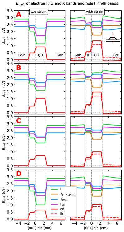 |
We start with the single-particle confinement potentials () for electrons and holes and show the results in Fig. 4 for along the QD growth axis parallel to [001] crystal direction, computed without and with the inclusion of elastic strain. We firstly notice that the strain has considerable effect on except for X[100]/[010] states which are bound inside QD body and for which attains the lowest energy in our structure, similarly to (In,Ga)As/GaP QDs Robert et al. (2012, 2014, 2016). On the other hand, the bands which are influenced much more by strain are X[001] and particularly , for which the strain can even revert the position of the minimum of outside of QD body. For the former (X[001]), the minimum of occurs above QD due to the tensile strain exerted by the dot body. We note that similar effect occurs also in SiGe/Si Klenovský et al. (2012) and (In,Ga)As/GaP Robert et al. (2014) QD systems. For the latter () the minimum is found in the GaAs-IL for Sb rich dots. As shown in Ref. Sala (2018), during the growth an Sb-soaking after the GaAs-IL deposition is employed prior to QD-nucleation. This is very likely to trigger an As-for-Sb anion exchange reaction at the GaAs-IL surface, leading to GaSb formation and thus a considerable material intermixing in the QD layer. Therefore, such intermixing leads there to the minimum of for -electrons () to be strongly positionally dependent in In1-xGaxAsySb1-y/GaAs/GaP QDs. Finally, we note that for L bands are affected by a mere increase in energy.
V Results for single-particle states
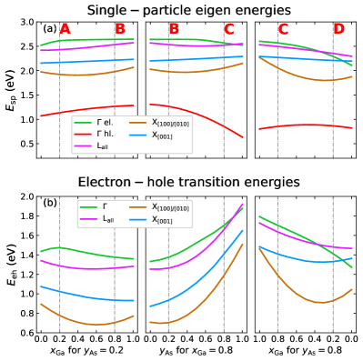 |
We now proceed with the results for single-particle states of our In1-xGaxAsySb1-y/GaAs/GaP QDs. For the alloys listed in table 1 we show the results for -, L-, and X-electron and -hole ground state energies () and the related interband transition energies () in Fig. 5. First of all, we observe that the first eight states involving L-electrons are almost degenerate in energy, hence, we do not distinguish between them in Fig. 5 and group them under the label Lall. The same holds true for (X[100], X010]) electrons, which we denote X[100]/[010]. Interestingly, for -electron states crosses that for Lall close to point C in the middle panel of Fig. 5 (a) and both Lall and X[001] close to point D in the rightmost panel of Fig. 5 (a).
However, since of electrons does not change considerably with dot composition, between electrons and holes is dictated by of the latter, see Fig. 5 (b). The energy of holes is mainly influenced by antimony content which is, indeed, one of the main features of our QD system and it will be important also when using of our dots for information storage in QD-Flash memory and for the quantum gate proposal are discussed later. The energies of holes, thus, cause the large increase in of 500 meV for recombinations between -electron to -hole states or even up to 700 meV for transitions from X[100]/[010], see middle panel of Fig. 5 (b). On the other hand, of electrons dictates the energy ordering of which is for most Ga and As concentrations from highest to lowest: , Lall, X[001], and X[100]/[010], see Fig. 5 (b). This is also the case for the energy flipping of for transitions from and Lall or X[001] to holes.
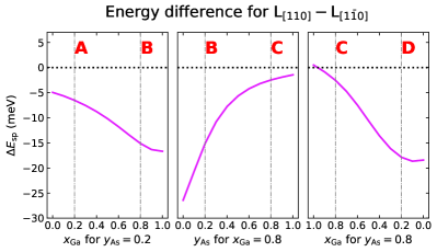 |
For completeness, we find the energy difference () between and , and , and and electrons to be smaller than in our structure. However, attains values of several tens of meV when computed between and bands, see Fig. 6. Clearly, for electrons is smaller than for , which is a result of the combined effect of shear strain, see Eq. (7), and piezoelectricity, Eqs. (10) and (11), for strained QDs fabricated from zincblende crystals due to their non-centrosymmetricity. The energy splitting seen in Fig. 6 is computed without taking into account mixing of L-Bloch waves with other electron bands which should be, however, rather small Robert et al. (2016).
We note, that we were able to observe transitions like those shown in Fig. 5 by PL for two samples with In0.2Ga0.8As0.8Sb0.2/GaAs/GaP and In0.5Ga0.5As/GaAs/GaP QDs, respectively, in Ref. Arx (a). A suitable method to observe transitions between -electrons and -holes, is a resonant PL technique similar, e. g., to that used in Ref. Rautert et al. (2019) for study of (In,Al)As/AlAs QDs.
 |
 |
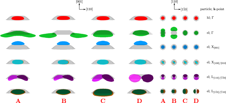
We proceed with the inspection of the wavefunctions of In1-xGaxAsySb1-y/GaAs/GaP QDs for and corresponding to A, B, C, and D (see Tab. 1), and we show that in Fig. 7. We find that the spatial location of the probability densities of states confirms our expectations drawn from the inspection of in Fig. 4. In particular, it allows us to make an assignment of the type of confinement of the -electrons in real space. Thus, C and D contents seem to correspond to type-I transition of -electrons to -holes, while B is type-II, and A corresponds to the transition between those two types of confinement. Further, the spatial position of wavefunctions shows that transitions involving X[001]-electrons are of type-II, and those for Lall and X[100]/[010] of type-I nature in real space, regardless of and contents in the dot.
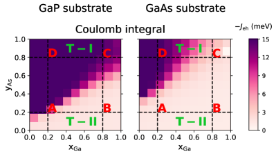
However, the assignment of -transitions can be done more precisely based on the inspection of the corresponding electron-hole Coulomb integrals (), see Fig. 8. We see that is by far smaller for type II compared to type I, owing to the spatial separation of the quasiparticles. Clearly, type I occurs in our system for dots rich in Indium and Arsenic, while those with larger Ga and Sb tend to be type-II. Notice also the comparison between GaP and GaAs substrates in Fig. 8. We will return to the identification of the type of confinement from the properties of excitons in the following.
V.1 Hole localization energies and storage time
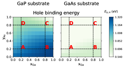 |
The variations of the QD valence bandedge energies upon chemical composition translates into a large variation of the hole localization energy defined by Marent (2010); Sala (2018); Sala et al. (2018) with being energy of the single-particle hole state and the substrate material -VB energy, respectively. The results for are shown in Fig. 9 as function of composition in In1-xGaxAsySb1-y QDs on GaAs-IL grown either on GaP or GaAs substrates. Evidently, the QDs grown on GaP exhibit more than twice compared to QDs on GaAs, thus, confirming the importance of substrate material for QD-Flash concept Nowozin (2013); Sala et al. (2016); Sala (2018); Sala et al. (2018).
The energy can be translated into the storage time of QD-Flash memory units by using the expression Marent (2010); Nowozin (2013); Marent et al. (2011); Sala (2018)
| (19) |
with depending on the bulk material valence -band effective mass , being the Boltzmann constant, the capture cross-section, and the temperature. If we let to depend on and and choose cm2 from Ref. Sala (2018); Sala et al. (2018) we find that the maximum eV in Fig. 9 relates to a storage time of 5000 s, occurring for pure GaSb QD with GaAs-IL grown in GaP. However, is a sensible parameter entering the calculation of the storage-time: it depends on the chemical composition and the QD-morphology itself (cmp. Ref. Bonato et al. (2015): cm2 and Ref. Sala et al. (2018): cm2). Both properties, and , are subject of constant technological optimization. Note that the value of is not part of our modelling scheme but enters the calculation as external parameter Nowozin (2013).
VI -excitons
We utilize the obtained single-particle wavefunctions as basis states for CI calculations and compute the corresponding exciton () states. Since we previously set , it is reasonable to evaluate in the following consisting of -electrons and -holes only to avoid omission of some Coulomb elements for complexes involving electrons.
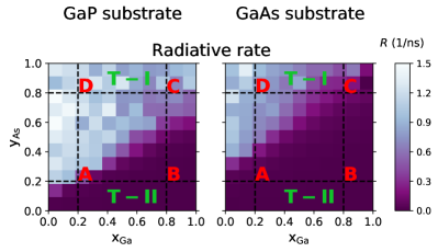 |
We first discuss the emission radiative rate () of calculated using the Fermi’s Golden rule as was discussed earlier, see also Ref. Klenovský et al. (2017) for details. The results for a number of and values are shown in Fig. 10, and together with Fig. 8, allow us to find the contents for which In1-xGaxAsySb1-y/GaAs/GaP QDs show type-I or type-II confinement. Type I can be expected for and consequently type II for . We also show in Fig. 10 the values of for the same dots on GaAs substrate for comparison. As expected, type II is associated with the amount of GaSb in the QD structure as found also elsewhere Klenovský et al. (2010a, b). Interestingly, type I for GaAs substrate occurs mostly for QDs with larger values of than for GaP substrate. This is again a result of much increased hydrostatic strain in the latter case, since the GaP substrate provides a considerably larger confinement for quasiparticles than the former. The aforementioned hints to the conclusion that QD structures grown on GaP might perform even better in optoelectronic applications than those grown on GaAs substrates which are currently under study Fischbach et al. (2017).
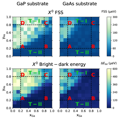 |
We now proceed with the fine structure of . That is caused in (In,Ga)As/GaAs QDs Schliwa et al. (2009); Křápek et al. (2015, 2016) by the effects of isotropic and anisotropic exchange interaction, which is the case also for the present system. The former causes the energy separation of bright and dark () while the latter results in FSS of .
The results for our dots are shown in Fig 11, again for both GaP and GaAs substrates in left and right panels, respectively. We find FSS of to be in the range of eV and of eV for both substrates in type-I regime. On the other hand, for type II those parameters drop to values eV. We note that the calculations of FSS and shown in Fig. 11 were performed with two electron and two hole single-particle basis states and expanded the exchange interaction into a multipole series Takagahara (1993); Křápek et al. (2015). Following Ref. Křápek et al. (2015) we considered the following terms of that expansion: monopole-monopole (EX0), monopole-dipole (EX1), and dipole-dipole (EX2). We find that irrespective of the substrate material (GaP or GaAs) the FSS in our system is dominated by EX2. On the other hand, EX0 and EX1 contribute to FSS and of only eV ( eV) and eV ( eV), respectively, for type-I (type-II) confinement. We further note that considerably smaller FSS for type II corroborates with the results of Refs. Křápek et al. (2015, 2016); Klenovský et al. (2015) for (In,Ga)As/Ga(As,Sb)/GaAs QDs and, in turn, confirms that to be a rather general property of dots which are type-II in real space.
The correlation is obtained in our CI calculations through admixing of excited single-particle states Klenovský et al. (2017). By taking the basis of two (six) ground state electron and two (six) hole states for calculations without (with) the effects of correlation, we have found the effect on FSS and energies to be eV (not shown). In total, the above findings make In1-xGaxAsySb1-y QDs with GaAs IL on GaP substrate a promising candidate for realization of optically bright single photon sources, different to type-I (In,Ga)As/GaAs QDs which are currently being under investigation as sources of light for quantum cryptography applications Fischbach et al. (2017); Paul et al. (2017); Schlehahn et al. (2018).
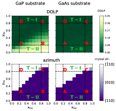 |
Furthermore, we would like to provide a useful way of experimental determination the type of confinement in In1-xGaxAsySb1-y/GaAs/GaP QDs based on measurement of the polarization of emission of , motivated by Ref. Klenovský et al. (2015). For the incoherent sum of the bright doublet, we show in Fig. 12 the polarization azimuth and the degree of linear polarization (DOLP), defined by
| (20) |
where and denote the maximum and minimum value of , respectively. Note that the azimuth is given in terms of the crystallographic axes in order to ease the comparison with the shape of the wavefunctions, shown in Fig. 7. Similarly as in Ref. Klenovský et al. (2015), we find that the azimuth of in type-II regime follows the orientation of the elongation of the wavefunction of the quasiparticle which is outside of the dot body. Contrary to Ref. Klenovský et al. (2015), in the present system the quasiparticles outside of QD are electrons which are elongated along axis, hence, the orientation of the azimuth in type II. In type I, on the other hand, the azimuth is dictated by the anisotropy of hole wavefunctions which is along axis. Thus, the flip of the polarization azimuth of emission from In1-xGaxAsySb1-y/GaAs/GaP QDs, when going from type I to type II, is a clear sign of the type of confinement.
On the other hand, DOLP of the incoherently summed is close to zero in type-I In1-xGaxAsySb1-y QDs on GaAs IL irrespective of the substrate. However, that is approaching for type II () in case of QDs grown on GaP substrate but not on GaAs. This is a consequence of the GaAs IL in In1-xGaxAsySb1-y/GaAs/GaP QDs providing additional confinement for -electrons which is not present, however, if the substrate is GaAs instead of GaP.
We note that the values of FSS, and DOLP, might be slightly different in dots which do not have uniform alloy content or are elongated.
For the sake of completeness, we note that the results corresponding to fine-structure, Fig. 11, can be confirmed experimentally, e. g., by resonant PL Rautert et al. (2019); Arx (b). The results discussed in Fig. 12 were in part observed in emission of type-I In1-xGaxAsySb1-y/GaAs/GaP QDs in Ref. Arx (a).
VII Application as quantum gates
The separation of -electron wavefunctions that are type-II in real space for structure B (see Tab. 1) into two segments, seen in Fig. 7, is qualitatively similar to that occurring for hole states in type-II (In,Ga)As QDs overgrown with Ga(As,Sb) layer Klenovský et al. (2010b). The electron wavefunctions form molecular-like states, in the sense that the four lowest energy states of a complex of two interacting electrons forms a singlet and a triplet Burkard et al. (1999); Klenovský et al. (2016). Hence, we tested the proposal of quantum gate (QG) given by Burkard et al. in Ref. Burkard et al. (1999) on our system. We note that the qubit discussed by Burkard et al. is based on the electron spin and it works by changing the sign of the exchange energy { () is the energy of triplet (singlet)} of two electron complex in QD by magnetic flux density () applied along [001] crystal direction. The necessary requirement for the correct operation of QG under consideration is that the lowest energy state of the two electron complex for T is singlet, i.e., a highly entangled spin state Burkard et al. (1999).
We test two In0.5Ga0.5Sb/GaAs/GaP QD structures: (i) QD1 with properties given in Fig. 2 (c) and (ii) QD2 with base diameter nm, height nm, and positioned on 3 ML thick GaAs IL. Note that both QD1 and QD2 are defined in GaP substrate and have and . The choice of was made in order to “push” -electron wavefunction towards GaAs IL, while is chosen to be some mean content mainly due to the fact that this parameter is not critical for the operation of our QG. We then apply on QD1 and QD2 in [001] direction, taking into account the Zeeman-Hamiltonian in single-particle eight-band calculations for -electrons. Note that due to the multiband we allowed also for coupling of electrons to valence band states. The states of two electron complexes is then computed by CI with four electron single-particle basis states.
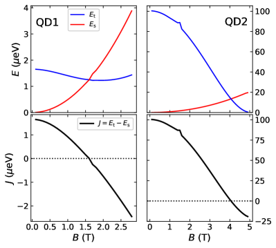 |
The results shown in Fig. 13 demonstrate that, for both QD1 and QD2, the lower energy state at T is singlet and that one can tune by increasing reaching crossing through zero at T and T, respectively. Note that, while tuning range of is considerably larger for QD2, the crossing occurs at larger as well.
| QD1 | QD2 | Ref. Burkard et al. (1999) | |
|---|---|---|---|
| () | 1.7 | 100 | 700 |
| (meV) | 14 | 8 | 3 |
| (nm) | 9.1 | 12 | 20 |
| 1.2 | 0.9 | 0.7 | |
| (%) | 0.4 | 5 | 20 |
To see the reason for that, we show in table 2 the comparison of results for QD1 and QD2. We choose similar parameters as in Ref. Klenovský et al. (2016) defined in Burkard et al. (1999): for T denoted by ; being the energy difference between the single-particle electron state belonging to Bloch wave with -symmetry and that with -symmetry to which the electron might escape, e. g., due to thermal radiation; the effective Bohr radius of the two electron complex where is the -point electron effective mass in GaAs Vurgaftman et al. (2001) and is the mass of free electron; ratio of where is half of the distance between the wavefunction segments; is the ratio of the probability density in the middle between the segments to the maximum probability density, which characterizes the coupling of the electrons. Clearly, QD2 seems to be more favorable for a realization of QG than QD1 which behaves somewhat on the borderline between electron quantum “molecule” and two uncoupled QDs. We show in Tab. 2 also the corresponding values of Burkard et al. Burkard et al. (1999). It is interesting to note that roughly corresponds to the maximum operational temperature which can be for QD1 and QD2 obtained by dividing by Boltzmann constant leading to values of K and K, respectively, both of which are higher than liquid nitrogen temperature.
Due to low coupling of the spins of electrons to that of the atomic nuclei, the In1-xGaxAsySb1-y/GaAs/GaP QD system provides potentially much lower dephasing Burkard et al. (1999) than the (In,Ga)As/Ga(As,Sb)/GaAs QDs studied in Ref. Klenovský et al. (2016), where QG was based on the spin of holes. However, clear disadvantage of the current proposal lies in the fact that -electrons are not the ground state for that quasiparticle, see Fig. 5 which might influence the way the two electron state is initialized in our QG. One possibility of overcoming that is to put QG into intrinsic part of PIN diode and utilize the effect of quantum tunneling by setting an appropriate voltage similarly as it is done in the QD-Flash memory concept Sala (2018). Another drawback then, however, lies in the time the two electrons will stay in -band in IL until they are scattered, e. g., to -indirect states. Here the mixing of those with ones will be important and following Ref. Diaz and Bryant (2006) that will be unfortunately more pronounced for QD2 because of its smaller size compared to QD1. Nevertheless, we believe that our system is an interesting alternative for QG realization.
VIII Conclusions
Studies of the electronic structure of In1-xGaxAsySb1-y/GaAs quantum dots grown either on GaP or GaAs substrates are presented. We first determine the confinement potentials for and conduction and valence bands. The latter along with the calculated single-particle hole states enable us to determine the most promising candidate structures for the realization of the QD-Flash memory concept from this system. Based on the calculated confinement potentials, we proceed with the determination of single-particle electron and hole states and the energy ordering of their mutual transitions. Here, we thoroughly discuss the method of calculations for -indirect transitions, and determine the form of the momentum matrix element that needs to be determined for such calculations to be correct. For transitions between -electron and -hole states we compute also the excitonic states. Through investigation of their emission rates, we identify for which concentrations of dot material constituents type-I or type-II confinement should be expected, and we show FSS and bright-dark splitting including the effect of the multipole expansion of exchange interaction. Moreover, we provide a neat method to experimentally determine the type of confinement from the measurements of the polarization of photoluminescence. Finally, we consider using In1-xGaxAsySb1-y/GaAs/GaP quantum dots as quantum gates and discuss their properties.
In conclusion, comparing to the (In,Ga)As/GaAs system, we show that, despite the presence of -indirect transitions, In1-xGaxAsySb1-y/GaAs/GaP quantum dots are perhaps more useful for effective realization of most of the building blocks of quantum information technology based on quantum dots, like entangled-photon sources or qubits. Left for future investigations based on full-zone methods such as the empirical tight-binding are the effects of inter-valley coupling and the calculation of L/X to transition probabilities.
IX Acknowledgements
P.K. would like to acknowledge the help of Elisa Maddalena Sala, Petr Steindl, and Diana Csontosová with grammar and visual style corrections and for fruitful discussions. A part of the work was carried out under the project CEITEC 2020 (LQ1601) with financial support from the Ministry of Education, Youth and Sports of the Czech Republic under the National Sustainability Programme II. This project has received national funding from the MEYS and the funding from European Union’s Horizon 2020 (2014-2020) research and innovation framework programme under grant agreement No 731473. P.K. was supported through the project MOBILITY, jointly funded by the Ministry of Education, Youth and Sports of the Czech Republic under code 7AMB17AT044. The work reported in this paper was (partially) funded by project EMPIR 17FUN06 Siqust. This project has received funding from the EMPIR programme co-financed by the Participating States and from the European Union’s Horizon 2020 research and innovation programme.
References
- Liang and Bowers (2010) D. Liang and J. E. Bowers, Nature Photonics 4, 511 (2010).
- Hatami et al. (2003) F. Hatami, W. T. Masselink, L. Schrottke, J. W. Tomm, V. Talalaev, C. Kristukat, and A. R. Goni, Physical Review B 67, 085306 (2003).
- Leon et al. (1998) R. Leon, C. Lobo, T. P. Chin, J. M. Woodall, S. Fafard, S. Ruvimov, Z. Liliental-Weber, and M. A. Stevens Kalceff, Applied Physics Letters 72, 1356 (1998).
- Guo et al. (2009) W. Guo, A. Bondi, C. Cornet, H. Folliot, A. Létoublon, S. Boyer-Richard, N. Chevalier, M. Gicquel, B. Alsahwa, A. L. Corre, J. Even, O. Durand, and S. Loualiche, physica status solidi (c) 6, 2207 (2009).
- Shamirzaev et al. (2010) T. S. Shamirzaev, D. S. Abramkin, A. K. Gutakovskii, and M. A. Putyato, Applied Physics Letters 97, 023108 (2010).
- Umeno et al. (2010) K. Umeno, Y. Furukawa, N. Urakami, R. Noma, S. Mitsuyoshi, A. Wakahara, and H. Yonezu, Physica E: Low-dimensional Systems and Nanostructures 42, 2772 (2010).
- Fuchi et al. (2004) S. Fuchi, Y. Nonogaki, H. Moriya, A. Koizumi, Y. Fujiwara, and Y. Takeda, Physica E: Low-dimensional Systems and Nanostructures 21, 36 (2004).
- Nguyen Thanh et al. (2011) T. Nguyen Thanh, C. Robert, C. Cornet, M. Perrin, J. M. Jancu, N. Bertru, J. Even, N. Chevalier, H. Folliot, O. Durand, and A. Le Corre, Applied Physics Letters 99, 143123 (2011).
- Rivoire et al. (2012) K. Rivoire, S. Buckley, Y. Song, M. L. Lee, and J. Vuckovic, Physical Review B 85, 045319 (2012).
- Fukami et al. (2011) F. Fukami, K. Umeno, Y. Furukawa, N. Urakami, S. Mitsuyoshi, H. Okada, H. Yonezu, and A. Wakahara, physica status solidi (c) 8, 322 (2011).
- Robert et al. (2012) C. Robert, C. Cornet, P. Turban, T. Nguyen Thanh, M. O. Nestoklon, J. Even, J. M. Jancu, M. Perrin, H. Folliot, T. Rohel, S. Tricot, A. Balocchi, D. Lagarde, X. Marie, N. Bertru, O. Durand, and A. Le Corre, Physical Review B 86, 205316 (2012).
- Robert et al. (2014) C. Robert, M. O. Nestoklon, K. Pereira da Silva, L. Pedesseau, C. Cornet, M. I. Alonso, A. R. Goni, P. Turban, J. . M. Jancu, J. Even, and O. Durand, Applied Physics Letters 104, 011908 (2014).
- Robert et al. (2016) C. Robert, K. Pereira DaSilva, M. O. Nestoklon, M. I. Alonso, P. Turban, J. . M. Jancu, J. Even, H. Carrere, A. Balocchi, P. M. Koenraad, X. Marie, O. Durand, A. R. Goni, and C. Cornet, Physical Review B 94, 075445 (2016).
- Sala et al. (2016) E. M. Sala, G. Stracke, S. Selve, T. Niermann, M. Lehmann, S. Schlichting, F. Nippert, G. Callsen, A. Strittmatter, and D. Bimberg, Applied Physics Letters 109, 102102 (2016).
- Sala (2018) E. M. Sala, Ph.D. thesis, Technische Universität Berlin (2018).
- Sala et al. (2018) E. M. Sala, I. F. Arikan, L. Bonato, F. Bertram, P. Veit, J. Christen, A. Strittmatter, and D. Bimberg, Physica Status Solidi B , 1800182 (2018).
- Arx (a) Petr Steindl, Elisa Maddalena Sala, Benito Alén, David Fuertes Marrón, Dieter Bimberg, Petr Klenovský, Phys. Rev. B submitted, arXiv:1906.09842 (a).
- Kapteyn et al. (1999) C. M. A. Kapteyn, F. Heinrichsdorff, O. Stier, R. Heitz, M. Grundmann, N. D. Zakharov, D. Bimberg, and P. Werner, Phys. Rev. B 60, 14265 (1999).
- Marent et al. (2011) A. Marent, T. Nowozin, M. Geller, and D. Bimberg, Semiconductor Science and Technology 26, 014026 (2011).
- Bonato et al. (2016) L. Bonato, I. F. Arikan, L. Desplanque, C. Coinon, X. Wallart, Y. Wang, P. Ruterana, and D. Bimberg, physica status solidi (b) 253, 1877 (2016).
- (21) Marent A., and Bimberg D. US patent 9.424,925, dated March 29, 2012.
- Stracke et al. (2014) G. Stracke, E. M. Sala, S. Selve, T. Niermann, A. Schliwa, A. Strittmatter, and D. Bimberg, Appl. Phys. Lett. 104, 123107 (2014).
- Stracke et al. (2012) G. Stracke, A. Glacki, T. Nowozin, L. Bonato, S. Rodt, C. Prohl, A. Lenz, H. Eisele, A. Schliwa, A. Strittmatter, U. W. Pohl, and D. Bimberg, Applied Physics Letters 101, 223110 (2012).
- Abramkin et al. (2014) D. S. Abramkin, V. T. Shamirzaev, M. A. Putyato, A. K. Gutakovskii, and T. S. Shamirzaev, JETP Lett. 88, 155319 (2014).
- Fry et al. (2000) P. W. Fry, I. E. Itskevich, D. J. Mowbray, M. S. Skolnick, J. J. Finley, J. A. Barker, E. P. O’Reilly, L. R. Wilson, I. A. Larkin, P. A. Maksym, M. Hopkinson, M. Al-Khafaji, J. P. R. David, A. G. Cullis, G. Hill, and J. C. Clark, Phys. Rev. Lett. 84, 733 (2000).
- Grundmann et al. (1995) M. Grundmann, O. Stier, and D. Bimberg, Phys. Rev. B 52, 11969 (1995).
- Klenovský et al. (2018) P. Klenovský, P. Steindl, J. Aberl, E. Zallo, R. Trotta, A. Rastelli, and T. Fromherz, Physical Review B 97, 245314 (2018).
- Birner et al. (2007) S. Birner, T. Zibold, T. Andlauer, T. Kubis, M. Sabathil, A. Trellakis, and P. Vogl, IEEE Trans. El. Dev. 54, 2137 (2007).
- (29) See Supplemental Material at [URL will be inserted by the production group] for the derivation of the formula given by Eq. (2) and the values of the material parameters used in the calculations.
- Luttinger (1956) J. M. Luttinger, Physical Review 102, 1030 (1956).
- Varshni (1967a) Y. P. Varshni, Physica 34, 149 (1967a).
- Dresselhaus et al. (1955) G. Dresselhaus, A. F. Kip, and C. Kittel, Physical Review 98, 368 (1955).
- Wei and Zunger (1998) S. H. Wei and A. Zunger, Applied Physics Letters 72, 2011 (1998).
- Wei and Zunger (1999) S. H. Wei and A. Zunger, Physical Review B 60, 5404 (1999).
- Van De Walle (1989) C. G. Van De Walle, Physical Review B 39, 1871 (1989).
- Klenovský et al. (2012) P. Klenovský, M. Brehm, V. Křápek, E. Lausecker, D. Munzar, F. Hackl, H. Steiner, T. Fromherz, G. Bauer, and J. Humlíček, Physical Review B 86, 115305 (8 pp.) (2012).
- Zibold (2007) T. Zibold, Ph.D. thesis, Technische Universität München (2007).
- (38) P.Y. Yu, M. Cardona, Fundamentals of Semiconductors (Springer, Berlin, 2001).
- (39) P. A. M. Dirac, The Principles of Quantum Mechanics (Oxford University Press, New York, 1958).
- (40) L. D. Landau, E. M. Lifshits, Course of Theoretical Physics 2: Quantum Mechanics (Pergamon, London, 1965).
- Wang and Zunger (1997) L. W. Wang and A. Zunger, Physical Review B 56, 12395 (1997).
- Wang et al. (1997) L. W. Wang, A. Franceschetti, and A. Zunger, Physical Review Letters 78, 2819 (1997).
- Landsberg and Adams (1973) P. T. Landsberg and M. J. Adams, Journal of Luminescence 7, 3 (1973).
- Varshni (1967b) Y. P. Varshni, Physica Status Solidi 19, 459 (1967b).
- Diaz and Bryant (2006) J. G. Diaz and G. W. Bryant, Physical Review B 73, 075329 (2006).
- Enders et al. (1995) P. Enders, A. Bärwolff, M. Woerner, and D. Suisky, Phys. Rev. B 51, 16695 (1995).
- Pollak (1990) F. H. Pollak, Semicond. Semimet. 32, 17 (1990).
- Enders (1995) P. Enders, phys. stat. sol. (b) 187, 541 (1995).
- Gershoni et al. (1993) D. Gershoni, C. H. Henry, and G. A. Baraff, IEEE J. of Quant. Elec. 29, 2433 (1993).
- Stier and Bimberg (1997) O. Stier and D. Bimberg, Phys. Rev. B 55, 7726 (1997).
- Jiang and Singh (1997) H. Jiang and J. Singh, Phys. Rev. B 56, 4696 (1997).
- Pryor (1998) C. Pryor, Phys. Rev. B 57, 7190 (1998).
- Stier et al. (1999) O. Stier, M. Grundmann, and D. Bimberg, Phys. Rev. B 59, 5688 (1999).
- Majewski et al. (2004) J. A. Majewski, S. Birner, A. Trellakis, M. Sabathil, and P. Vogl, phys. stat. sol. (c) 8, 2003 (2004).
- Winkelnkemper et al. (2006) M. Winkelnkemper, A. Schliwa, and D. Bimberg, Phys. Ref. B 74, 155322 (2006).
- Bahder (1990) T. B. Bahder, Phys. Rev. B 41, 11992 (1990).
- Schliwa et al. (2007) A. Schliwa, M. Winkelnkemper, and D. Bimberg, Physical Review B 76, 205324 (2007).
- Pryor et al. (1998) C. Pryor, J. Kim, L. W. Wang, A. J. Williamson, and A. Zunger, J. {A}ppl. {P}hys. 83, 2548 (1998).
- Bardeen and Shockley (1950) J. Bardeen and W. Shockley, Phys. Rev. 80, 72 (1950).
- Herring and Vogt (1956) C. Herring and E. Vogt, Physical Review 101, 944 (1956).
- Chao and Chuang (1992) C. Y.-P. Chao and S. L. Chuang, Physical Review B 46, 4110 (1992).
- Cady (1946) W. F. Cady, Piezoelectricity (McGraw-Hill, 1946).
- Schliwa et al. (2009) A. Schliwa, M. Winkelnkemper, and D. Bimberg, Phys. Rev. B 79, 075443 (2009).
- Bester et al. (2006) G. Bester, X. Wu, D. Vanderbilt, and A. Zunger, Phys. Rev. Lett. 96, 187602 (2006).
- Beya-Wakata et al. (2011) A. Beya-Wakata, P. Y. Prodhomme, and G. Bester, Physical Review B 84, 195207 (2011).
- Braskén et al. (2000) M. Braskén, M. Lindberg, D. Sundholm, and J. Olsen, Phys. Rev. B 61, 7652 (2000).
- Shumway et al. (2001) J. Shumway, A. Franceschetti, and A. Zunger, Phys. Rev. B 63, 155316 (2001).
- Stier et al. (2001) O. Stier, A. Schliwa, R. Heitz, M. Grundmann, and D. Bimberg, phys. stat. sol. (b) 224, 115 (2001).
- Klenovský et al. (2017) P. Klenovský, P. Steindl, and D. Geffroy, Scientific Reports 7, 45568 (2017).
- Bester (2008) G. Bester, Journal of Physics: Condensed Matter 21, 023202 (2008).
- Benedict (2002) L. X. Benedict, Phys. Rev. B 66, 193105 (2002).
- Luo et al. (2009) J.-W. Luo, G. Bester, and A. Zunger, New Journal of Physics 11, 123024 (2009).
- Stier (2000) O. Stier, Ph.D. thesis, Technische Universität Berlin (2000).
- Rautert et al. (2019) J. Rautert, T. S. Shamirzaev, S. V. Nekrasov, D. R. Yakovlev, P. Klenovsky, Y. G. Kusrayev, and M. Bayer, Physical Review B 99, 195411 (2019).
- Marent (2010) A. Marent, Ph.D. thesis, Technische Universität Berlin (2010).
- Nowozin (2013) T. Nowozin, Ph.D. thesis, Technische Universität Berlin (2013).
- Bonato et al. (2015) L. Bonato, E. M. Sala, G. Stracke, T. Nowozin, A. Strittmatter, M. N. Ajour, K. Daqrouq, and D. Bimberg, Applied Physics Letters 106, 042102 (2015).
- Klenovský et al. (2010a) P. Klenovský, V. Křápek, D. Munzar, and J. Humlíček, Quantum Dots 2010 245, 012086 (2010a).
- Klenovský et al. (2010b) P. Klenovský, V. Křápek, D. Munzar, and J. Humlíček, Applied Physics Letters 97, 203107 (2010b).
- Fischbach et al. (2017) S. Fischbach, A. Schlehahn, A. Thoma, N. Srocka, T. Gissibl, S. Ristok, S. Thiele, A. Kaganskiy, A. Strittmatter, T. Heindel, S. Rodt, A. Herkommer, H. Giessen, and S. Reitzenstein, Acs Photonics 4, 1327 (2017).
- Křápek et al. (2015) V. Křápek, P. Klenovský, and T. Šikola, Physical Review B 92, 195430 (2015).
- Křápek et al. (2016) V. Křápek, P. Klenovský, and T. Šikola, Acta Physica Polonica A 129, A66 (2016).
- Takagahara (1993) T. Takagahara, Physical Review B 47, 4569 (1993).
- Klenovský et al. (2015) P. Klenovský, D. Hemzal, P. Steindl, M. Zíková, V. Křápek, and J. Humlíček, Physical Review B 92, 241302(R) (2015).
- Paul et al. (2017) M. Paul, F. Olbrich, J. Hoeschele, S. Schreier, J. Kettler, S. L. Portalupi, M. Jetter, and P. Michler, Applied Physics Letters 111, 033102 (2017).
- Schlehahn et al. (2018) A. Schlehahn, S. Fischbach, R. Schmidt, A. Kaganskiy, A. Strittmatter, S. Rodt, T. Heindel, and S. Reitzenstein, Scientific Reports 8, 1340 (2018).
- Arx (b) Marcus Reindl, Jonas H. Weber, Daniel Huber, Christian Schimpf, Saimon F. Covreda Silva, Simone L. Portalupi, Rinaldo Trotta, Peter Michler, and Armando Rastelli submitted, arXiv:1901.11251 (b).
- Burkard et al. (1999) G. Burkard, D. Loss, and D. P. DiVincenzo, Physical Review B 59, 2070 (1999).
- Klenovský et al. (2016) P. Klenovský, V. Křápek, and J. Humlíček, Acta Physica Polonica A 129, A62 (2016).
- Vurgaftman et al. (2001) I. Vurgaftman, J. R. Meyer, and L. R. Ram-Mohan, Journal of Applied Physics 89, 5815 (2001).