Comprehensive tunneling spectroscopy of
quasi-freestanding MoS2 on graphene on Ir(111)
Abstract
We apply scanning tunneling spectroscopy to determine the bandgaps of mono-, bi- and trilayer MoS2 grown on a graphene single crystal on Ir(111). Besides the typical scanning tunneling spectroscopy at constant height, we employ two additional spectroscopic methods giving extra sensitivity and qualitative insight into the -vector of the tunneling electrons. Employing this comprehensive set of spectroscopic methods in tandem, we deduce a bandgap of eV for the monolayer. This is close to the predicted values for freestanding MoS2 and larger than is measured for MoS2 on other substrates. Through precise analysis of the ‘comprehensive’ tunneling spectroscopy we also identify critical point energies in the mono- and bilayer MoS2 band structures. These compare well with their calculated freestanding equivalents, evidencing the graphene/Ir(111) substrate as an excellent environment upon which to study the many feted electronic phenomena of monolayer MoS2 and similar materials. Additionally, this investigation serves to expand the fledgling field of the comprehensive tunneling spectroscopy technique itself.
I Introduction
The various exciting properties of monolayer molybdenum disulfide (ML-MoS2), the paradigmatic semiconducting transition metal dichalcogenide (TMDC), are well-documented Ganatra and Zhang (2014); Manzeli et al. (2017). Amongst these its large, direct bandgap is promising for the electronics communities, and is a basic quality to be characterized. Large-scale flakes can be grown epitaxially Hall et al. (2018); Najmaei et al. (2013); Li et al. (2018) or exfoliated Novoselov et al. (2005); Radisavljevic et al. (2011), but reliable characterization of the pristine electronic bandgap remains problematic.
Optical measurements are influenced by the large exciton binding energy of ML-MoS2. Standard angle-resolved photoemission spectroscopy (ARPES) has no access to the conduction band unless it is shifted below the Fermi energy through heavy doping. This, however, also leads to band distortion and bandgap renormalization due to the change in dielectric environment Miwa et al. (2015); Ehlen et al. (2018); Liang and Yang (2015); Erben et al. (2018). Pump-probe ARPES can measure the electronic bandgap Grubišić Čabo et al. (2015), but suffers from poor energy resolution.
Scanning tunneling spectroscopy (STS) can directly access the electronic density of states above and below , and it has indeed been performed on ML-MoS2 on a variety of substrates. However, the substrates — metallic by necessity — tend to screen, gate, and/or mechanically strain the MoS2. This leads to the predicted freestanding bandgap of eV Cheiwchanchamnangij and Lambrecht (2012); Qiu et al. (2013); Ramasubramaniam (2012); Shi et al. (2013) being considerably reduced. For example the bandgap measured by constant height STS is eV on an Au substrate Bruix et al. (2016), eV on graphene/SiC Liu et al. (2016), eV on quartz Rigosi et al. (2016), eV on graphene/Au Shi et al. (2016), and variously eV Lu et al. (2015), eV Zhang et al. (2014) or eV Huang et al. (2015) on graphite. In addition to simply reducing the bandgap size, substrate coupling will affect each band differently — due to the differing planar nature of the Mo and S orbitals, the band structure is distorted inhomogeneously across the MoS2 Brillouin zone (BZ) Bruix et al. (2016). Large bandgaps of eV Hong et al. (2018) and eV Krane et al. (2016) have been reported, but only in locations where the ML-MoS2 is locally decoupled from an inhomogeneous substrate. On top of all this, practical difficulties due to sulfur’s relatively high vapour pressure had, until recently Hall et al. (2018), hindered molecular beam epitaxy (MBE) synthesis of MoS2. Thus close-to-freestanding MoS2 flakes of sufficient size, quality, and cleanness on STS-permitting substrates have remained elusive.
Additional to the complications caused by the metallic substrates on which it is performed, there are shortcomings in the typical practice of STS. It has recently been shown by Zhang et al. Zhang et al. (2015) that constant height STS alone is insufficient for accurate bandgap determination, as states from the edge of the BZ can go undetected due to their reduced decay length. Therefore it remains an open question, how accurately the constant height STS measured bandgaps represent the magnitude of the ML-MoS2 direct gap. In contrast, constant current STS allows the tip to move closer to the sample to give access to these weaker signals, while mode STS (explained below) allows identification of the states’ location within the BZ.
In this work we present high-quality ML-, bilayer (BL-), and trilayer (TL-)MoS2 which is well decoupled from its graphene/Ir(111) substrate. Following the approach of Zhang et al. Zhang et al. (2015), we use ‘comprehensive STS’ (constant height, constant current and modes together) to identify not only the bandgaps but also various critical point energies (CPEs), i.e. local extrema in the band structure. These measured energies compare favourably with those of theoretical calculations for the freestanding materials, evidencing this system as an opportunity to study the inherent characteristics of mono- or few-layer MoS2 without obtrusive substrate effects.
Moreover, our analysis makes plain that standard constant height STS fails to detect both the valence band maximum and conduction band minimum, and thus does not measure the bandgap of ML-MoS2. This has implications for the interpretation of STS data of ML-MoS2, and indeed other materials with extremal points forming the bandgap at large parallel momenta. Comprehensive STS is not only more sensitive, but enables also the determination of the CPEs making up the tunneling spectrum. As shall be demonstrated here, this can prevent the false assignment of a band edge. It is thus a vital tool in the determination of the electronic structure of the semiconducting TMDCs. The technique and its associated analysis have only seen a few instances of usage Zhang et al. (2015, 2017); Krane et al. (2018), and so a broader implementation could be wished.
II Methods
The sample is prepared in situ at pressures mbar. The Ir(111) single crystal is cleaned by Ar+ ion sputtering and annealing at temperatures K. As described in Ref. Coraux et al. (2009), a closed monolayer of graphene (Gr) is grown on Ir(111) via temperature programmed growth and chemical vapour deposition (CVD) at K. ML- to few-layer MoS2 is subsequently grown on the Gr/Ir(111) substrate by van der Waals MBE, according to the methods developed in Ref. Hall et al. (2018). Mo is evaporated from an e-beam evaporator and S from FeS2 granules in a Knudsen cell. Specifically, we evaporate Mo in a S background pressure of mbar onto the room temperature substrate, and then anneal the system to K in the same S background pressure. The process of co-evaporation then annealing can be repeated in cycles, in order to promote well-oriented, multiple-layer growth.
Scanning tunneling microscopy (STM) and STS are performed at K and mbar with a tungsten tip. For STS we use a lock-in amplifier with modulation frequency Hz and modulation amplitudes mV — together with thermal broadening this yields experimental resolution of meV or better Morgenstern (2003). We perform comprehensive STS comprised of three different modes: constant height (recording ), constant current () and (), where is the tunneling current, the bias voltage and the tip-to-sample distance or ‘height’. The principles of these three modes shall be discussed.
For both constant height and constant current STS we measure the signal while is ramped, giving information on the local density of states of the sample Stroscio et al. (1986). Though constant height STS allows both valence and conduction bands to be measured in a single spectrum, certain states may go undetected if is too large. Constant current STS does not permit ramping across but offers greater dynamic range; the tip can move towards the sample and thereby detect some suppressed signals missed in constant height mode. This suppression can be due to the fact that a state with finite parallel momentum will decay into the vacuum with an inverse decay length
| (1) |
where is the free electron mass and is the bias-dependent tunneling barrier between tip and sample with work functions and respectively Feenstra et al. (1987); Tersoff and Hamann (1983). Thus, states at the edge of the BZ decay more quickly into the vacuum than those at the center. This necessitates the tip moving closer to detect them, especially if stabilization was performed at a voltage (energy) where -point states dominate.
We indirectly measure and thus through mode STS. Here the lock-in modulates the height ( pm) while is ramped at constant as before. Considering a tunneling current Tersoff and Hamann (1985) one finds
| (2) |
we measure this and thereby extract an effective tunneling decay constant. Through comparison with the spectra obtained via the two other modes, one can assign features of the STS spectra to particular critical points in the BZ. Thus, a degree of -space resolution has been added to the traditional STS. We note that inside the MoS2 bandgap, when the tip moves very close to the sample, the ‘thick barrier’ limit implicitly assumed in Eq. (2) does not necessarily hold and Gr states may contribute to the tunneling current. Therefore we do not draw inferences from values within the bandgap.
III Experimental Results
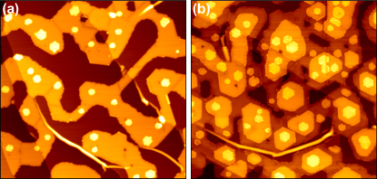
STM topographs of two typical MoS2 samples are shown in Fig. 1. In (a) an MoS2 coverage of around layers yields a network of ML-MoS2 extending over the Gr/Ir(111) substrate, crossing several Ir step edges. It is decorated by small BL islands of nm diameter. The cleanness and low defect density of the MoS2, reported previously Hall et al. (2018), were verified with STM here. Grain boundaries are visible between ML flakes of different orientation. The majority of these are mirror twin boundaries (MTBs), the properties of which are discussed in Ref. Jolie et al. (2019). In the lower section of the topograph a Gr wrinkle can be seen, resultant from the CVD growth.
With a higher coverage of approximately layers, shown in Fig. 1(b), the sample exhibits ML-, BL- and TL-MoS2 islands in coexistence. Small areas of exposed Gr are visible below the nearly-closed ML. Large, well-oriented BL and nm diameter TL islands form on top. MTBs are seen to also occur in the BL.
III.1 Constant height STS of mono- and bilayer MoS2
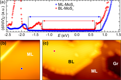
For illustrative purposes we first determine the bandgaps of ML- and BL-MoS2 using constant height STS only, as is typically done in the literature for this and other TMDCs. Fig. 2(a) shows two exemplary constant height spectra of ML- and BL-MoS2. Topographs in Fig. 2(b,c) show where the respective spectra were obtained. Note that all spectra in this work were recorded at locations at least nm from any defects — e.g. edges, MTBs, or point-defects — to avoid any perturbation or confinement effects which these may cause. As is common in the literature, we here define the band edges to be where the d/d signal becomes clearly discernible from background noise levels. Through this approach, we find the valence band maximum (VBM) to be located at eV and the conduction band minimum (CBM) to be at eV for ML-MoS2. Similarly for the BL, the corresponding band edges are found to be at eV and eV. This would yield bandgap estimates of eV and eV for ML- and BL-MoS2 respectively. However, it shall be demonstrated that these bandgap determinations for MoS2 are unreliable.
We briefly consider the band structures of ML- and BL-MoS2 close to , to guide proceeding STS analysis. The band structures sketched in Fig. 3 are based on previous density functional theory (DFT) calculations Cheiwchanchamnangij and Lambrecht (2012); Ramasubramaniam (2012); Qiu et al. (2013); Ramasubramaniam et al. (2011). As seen in Fig. 3(a), the ML has a direct bandgap located at the K-point. The VB is split by meV at K due to spin-orbit coupling, and a maximum at lies close in energy Cheiwchanchamnangij and Lambrecht (2012); Qiu et al. (2013); Ramasubramaniam (2012); Zhu et al. (2011); Ehlen et al. (2018). In contrast, the BL (b) has a smaller and indirect bandgap, with the VBM located at the -point and the CBM at the Q-point. The critical points at K and Q in the CB lie close in energy however, and so the true location of the CBM is debated in the literature Du et al. (2018); Liu et al. (2015). The VB is split at the -point due to interlayer hopping Debbichi et al. (2014).

III.2 Comprehensive STS of monolayer MoS2
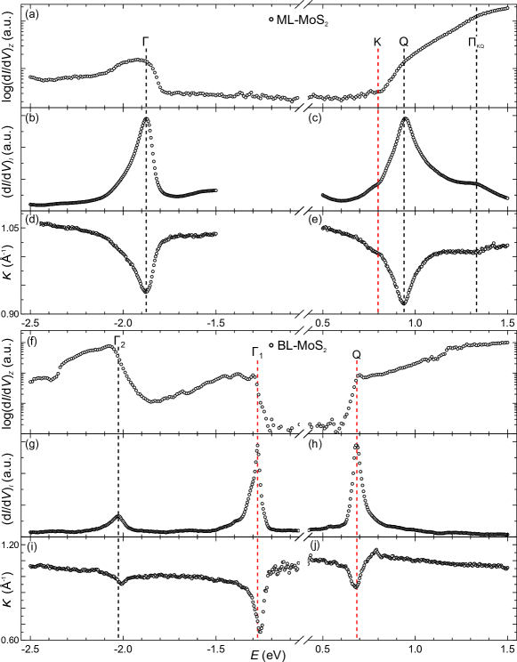
In Fig. 4 exemplary sets of comprehensive STS on ML- and BL-MoS2 are shown. The three different STS modes are considered together and for both the ML and BL are compared across at least five sets of spectra, taken on various islands and with different STM tips. Through this, some critical points in the respective band structures can be assigned.
Beginning with the VB of the ML, Fig. 4(a) shows the same constant height spectrum as in Fig. 2(a) now plotted logarithmically. In (b) constant current STS yields a main peak at eV with a slight shoulder towards larger binding energies. In (d) the corresponding measurement shows a dip, also at eV. This dip to indicates a sudden drop in the effective tunneling decay constant of the states there, i.e. states with less . (A discussion of the actual values extracted from follows in Sec. IV.) Considering the drop in and with reference to the band structure of ML-MoS2 [Fig. 3 (a)], we must assume this feature to be due to the -point. Though the VBM is expected to be the upper of the spin-split bands at the K-point, we can expect the spectrum to be totally dominated by states from . Firstly, the states at K decay faster into the vacuum due to their high . Furthermore, calculation has shown that the orbital character at the -point is predominantly Mo-d, while at K it is predominantly Mo-dxy,d, i.e. mostly out-of-plane and mostly in-plane respectively Komsa and Krasheninnikov (2013); Cappelluti et al. (2013); Padilha et al. (2014). Thus, if the bands at K and lie sufficiently close in energy we would expect the -band to mask the K-band in our STS signal. Indeed in ab initio calculations the separation between the upper K-band (K↑) and the band at is found variously to be around Cheiwchanchamnangij and Lambrecht (2012), Zhu et al. (2011), Ramasubramaniam (2012) or eV Qiu et al. (2013). We conclude that both branches of the spin-split band at K are masked by states. An estimate for the position of K↑ (i.e. the VBM) can nonetheless be made. In ARPES experiments on ML-MoS2 grown on Gr/Ir(111) by the same method as in this work, a separation between and K↑ of eV was found Ehlen et al. (2018); Ehlen . This energy separation would locate K↑ at eV in our case. We consider lower and upper bounds based on the aforementioned DFT calculations to be eV Cheiwchanchamnangij and Lambrecht (2012) and eV Qiu et al. (2013) respectively, i.e. for K↑ to lie between eV and eV. Taking these bounds as a conservative uncertainty, we estimate the VBM of our ML-MoS2 system to be located at eV.
The CB of ML-MoS2 also shows various features in constant current STS, Fig. 4(c). A main peak at eV is flanked by a small shoulder at eV and, towards higher energies, a broad hump at eV. In (e), shows a clear dip to at eV. Consulting the theoretical band structure [Fig. 3(a)], a local minimum close to the CB edge is expected at the Q-point, and any states are much further from the Fermi level — thus this feature must be assigned to the Q-point. Across our sets this peak tended to take one of two values — either eV or eV approximately — and typically has a broad shape suggestive of more than one contributing state. We find no correlation of the Q-point peak value to the lateral position in the MoS2 layer. The properties could be due to the spin-splitting of the band at the Q-point, predicted to be of magnitude eV Qiu et al. (2013); Ramasubramaniam (2012); Cheiwchanchamnangij and Lambrecht (2012); Zhu et al. (2011). The faint shoulder at eV has no obvious corresponding feature in (e) here, though a small peak was occasionally seen at this energy in spectra. The feature was practically undetectable in constant height STS, suggesting that it originates from states of large and/or of mostly in-plane orbital nature. This fact, combined with a small peak sometimes seen in and with consultation of the ML-MoS2 band structure, compels assigning this feature to states at the K-point. This represents the CBM of ML-MoS2, found at eV across the measured sets. This K-point extremum being detectable, in contrast to the K-point of the VB, can be explained by its orbital character. The K-point at the CBM is dominated by out-of-plane Mo-d orbitals; at the VBM it is dominated by in-plane Mo-dxy,d orbitals Komsa and Krasheninnikov (2013); Cappelluti et al. (2013); Padilha et al. (2014). Finally, we assign the broad hump at eV to the local maximum lying roughly halfway between the K- and Q-points, which we term . The (average) assigned CPEs for the ML are summarized in Table 1.
| (K↑) | K | Q | ||
|---|---|---|---|---|
| () |
It should be noted that the CPEs constituting band edges have alternatively been defined by Zhang et al. Zhang et al. (2015) to be at the midpoint of the transition from TMDC to substrate states in the STS signal. This is practically equivalent to us taking the energy at FWHM of the peaks closest to — for example in Fig.4(c), with Gaussians fitted to the various features including the K-point shoulder, this would yield a CBM at eV rather than eV. However, due to ambiguities of peak-fitting in our spectra and for simplicity, we chose instead to define the band edges at the peak centers in constant current STS.
III.3 Comprehensive STS of bilayer MoS2
In constant height STS of the BL-MoS2, Fig. 4(f), two sharp rises in intensity are seen in the VB. These are accompanied by clear peaks in constant current and clear dips in measurements, (g) and (i) respectively. Based on their nature and with consideration of the generic BL band structure [Fig. 3(b)], we can confidently assign the features marked at eV and eV to the split bands at the -point, labelled and respectively. The signal from is much weaker in constant current and STS because in the midst of the VB states the feedback loop has taken the tip further away from the sample, making it less sensitive to the onset of the -band. Also for this reason, and considering their faster decay into the vacuum, it is wholly unsurprising that the K-point states expected close to eV were not reliably detected.
Similarly in the CB a sharp rise in constant height [Fig. 4(f)] coincides with a peak in constant current (h) and dip in (j). The last of these indicates states from near the centre of the BZ. Consultation of Fig. 3(b) shows that -states lie deep in the CB, and thus we assign this feature at eV to the Q-point representing the CBM. The small peak in at around eV in (j) could possibly be due to the K-point minimum, but this feature was not observed consistently enough with different tips to allow an unambiguous deconvolution. Considering the Q-point states’ energetic proximity, their location at the band edge, and their smaller , they could be expected to mask the K-point states in STS. Indeed this issue is non-trivial; there is debate in the literature as to whether the CBM of BL-MoS2 lies at the K-point Chu et al. (2015); Cheiwchanchamnangij and Lambrecht (2012) or at the Q-point Du et al. (2018); Mak et al. (2010); Debbichi et al. (2014), a matter of relevance due to the lack of symmetry at the latter. The (average) assigned CPEs for the BL are summarized in Table 2.
| Q | ||
|---|---|---|
With the band extrema identified in Tables 1 and 2 we determine bandgaps of eV and eV. For the specific sets shown in Fig. 4 the bandgaps are eV and eV respectively.
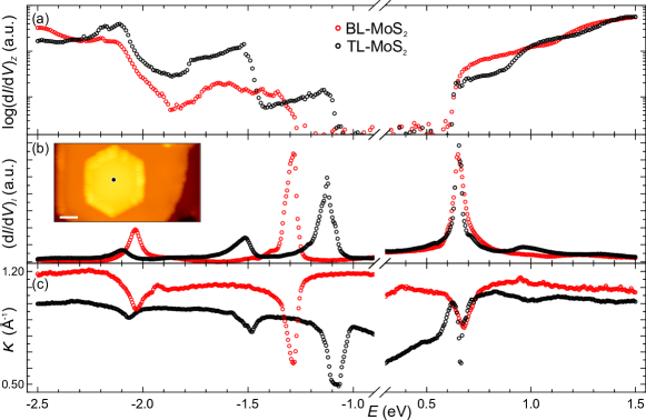
III.4 Comprehensive STS of trilayer MoS2
Fig. 5 shows comprehensive STS of TL-MoS2, together with a BL set for comparison. The small size of the TL islands — for example nm diameter in Fig. 5 — means that interfering quantum confinement effects cannot be ruled out. Nonetheless, some qualitative features are obvious from the spectroscopic data. Namely, a third branch in the VB has appeared due to further splitting of the band at , while the CB edge remains mostly unchanged, in line with theoretical calculations Padilha et al. (2014); Trainer et al. (2017). This is discussed further in Sec. IV. A bandgap of eV is estimated based on Fig. 5, though we provide this value tentatively due to limited statistics. Additionally, although investigations of such islands did not show lateral confinement, the aforementioned quantum-size issue should be noted.
IV Discussion
We find that using constant height STS alone would lead to a eV overestimation of (when compared with comprehensive STS analysis) because the measured states are not actually those at the respective band edges. In constant height STS both band extrema go undetected. In comprehensive STS the CBM at K is detected. The VBM is not detected but, importantly, a false assignment of the VBM is prevented through measurements. One could wrongly assume that the peak in Fig. 4(a,b) is due to the VBM (at the K-point), but the drop in rules this out. Put simply: comprehensive STS sees more states, and when it is blind to certain states then it can tell us that this is the case.
The benefits of the more thorough technique are further illustrated by accurate observation of layer-dependent phenomena in the MoS2. It is known from the literature that the bandgap reduction with increasing thickness is due to the VBM — specifically the -point — shifting to smaller binding energies, while the CBM does not change significantly in energy Padilha et al. (2014); Trainer et al. (2017); Bradley et al. (2015). Using only constant height STS the CBM appears to shift by eV towards upon addition of a second MoS2 layer, whereas the shift is indeed much less drastic ( eV) in comprehensive STS. The continuation of these trends — a static CBM and an up-shifting VBM — is visible as the thickness is increased from BL to TL [Fig. 5]. Additionally, the well-documented lifting of degeneracy in the -band and its consequent splitting from one (ML) to two (BL) to three (TL) branches is clearly visible across the data sets. Thereby the coupling of each newly added MoS2 layer to those underneath is seen through comprehensive STS.
The technique has its limitations, of course. As discussed, we could not unambiguously detect the K-point states which represent the VBM of ML-MoS2, presumably due to their short decay length, in-plane orbital character, and proximity to the dominating point. States being hidden due to a combination of these factors is an issue; previous comprehensive STS investigations of ML-MoS2 have also failed to identify the VBM Krane et al. (2018). The K-point VBM was clearly detected in ML-MoSe2 and ML-WSe2, presumably because in these cases it is separated from the -point by large energies of eV and eV respectively Zhang et al. (2015). However, the CBs of these materials and their sulfide analogues exhibit a trend — the K-point STS signal becomes less and less prominent as it moves energetically closer to the Q-point Zhang et al. (2015).
Measuring helps reveal a state’s location in the BZ, but extracting the corresponding values of proves non-trivial. In Eq. (1) the only unknown variable is the energy barrier . We can set this (to eV) to obtain reasonable values for most CPEs. However, this is an ad hoc adjustment and it fails for some CPEs regardless. Similar problems arise in measurements in the literature Zhang et al. (2015); Krane et al. (2018). The values of given here remain valid; we additionally take spectra at various bias voltages, to which is then fitted, showing excellent agreement with spectra. We suggest the difficulty in translating into actual values is due to an oversimplified picture of the tunneling that forms the basis of Eq. (1). Nonetheless, serves as a useful qualitative measure of a state’s position in the BZ relative to states energetically nearby.
A more puzzling issue is an apparent mismatch between STS and ARPES studies. Specifically, the -point in the VBM of ML-MoS2 on Gr/Ir(111) is found to be eV in STS (this work) but eV in ARPES Ehlen et al. (2018); Ehlen . The -points in BL-MoS2 on the same substrate coincide however; eV and eV in STS (this work) compared with eV and eV in ARPES Ehlen et al. (2018); Ehlen . In collaborative STS Bruix et al. (2016) and ARPES Miwa et al. (2015) investigation of ML-MoS2 on Au(111), discrepancies of eV and eV were found for the - and K-point respectively. Comprehensive STS on the same system showed further disagreement Krane et al. (2018). A comparative study of comprehensive STS and ARPES (performed on the same sample in the same UHV chamber) would present a considerable experimental challenge, but would be worthwhile if the community is to address these problems of inconsistency.
Despite the discussed experimental uncertainties, it is clear that ML-MoS2 on Gr/Ir(111) is a very well decoupled system. Our conservative estimate eV represents the largest STS-measured bandgap of ML-MoS2 on a homogeneous substrate. This value comes much closer to the freestanding eV predicted by DFT Cheiwchanchamnangij and Lambrecht (2012); Qiu et al. (2013); Ramasubramaniam (2012); Shi et al. (2013) than those of ML-MoS2 measured on other substrates, such as graphite ( eV Huang et al. (2015)). If we would instead take the bandgap size of eV based on constant height STS alone — as is done in the literature with which we compare this work — our system appears even better decoupled. ML-MoS2 nanopatches suspended over Au(111) vacancy islands of roughly nm diameter have shown an apparent bandgap of eV indicating that they are quasi-freestanding Krane et al. (2016), but their small size leaves them liable to lateral quantum confinement effects. An apparent bandgap of eV has been reported for water-intercalated areas of ML-MoS2 on graphite Hong et al. (2018). However, the interficial water layer and defects resultant from the wet transfer process have competing doping effects and leave the MoS2 inhomogeneous.
The freestanding nature of our system is further apparent upon closer examination of the measured CPE values. In Table 3 the energy separations of ML- and BL-MoS2 CPEs can be compared with those of various DFT calculations. Taking into account that there is considerable discrepancy within the DFT results themselves, the measured CPEs agree reasonably with calculation. The bandgap eV also compares well with values eV Cheiwchanchamnangij and Lambrecht (2012) and eV Debbichi et al. (2014) from the literature.
Previous experiments on ML-MoS2 on Gr/Ir(111) suggest weak substrate interaction also. MoS2 islands are mobile enough to be moved laterally on the surface using the STM tip Hall et al. (2018). Additional evidence of weak interaction was seen in photoluminescence spectroscopy, x-ray photoemission spectroscopy, temperature dependent Raman spectroscopy, and ARPES Ehlen et al. (2018). For example, comparing Raman measurements at room temperature and at K showed that the ML-MoS2 does not follow the thermal expansion of its substrate. Instead its expansion resembles that of a freestanding layer, meaning that it is not strained by the substrate. In ARPES, no hybridization of Gr and MoS2 bands was seen Ehlen et al. (2018).
| ML CB | ML CB | BL VB | |
| Ref. | (eV) | (eV) | (eV) |
| this work | |||
| Cheiwchanchamnangij and Lambrecht (2012) | , | ||
| Qiu et al. (2013) | , | - | |
| Ramasubramaniam (2012); Ramasubramaniam et al. (2011) | , | ||
| Zhu et al. (2011) | , | - | |
| Debbichi et al. (2014) | - | - |
V Conclusion
We have characterized the electronic structure of quasi-freestanding ML-, BL- and TL-MoS2 on Gr/Ir(111) with high-precision STS analysis, whereby the bandgaps have been determined, various CPEs close to identified, and layer-dependent phenomena observed. The measured bandgap sizes are close to those of the freestanding material, showing that MoS2 is well decoupled from this substrate. The measured CPEs can be cross-referenced with those predicted by DFT calculations from the literature, further corroborating this. Thus Gr/Ir(111) represents a substrate for STS investigations of the inherent properties of 2D-TMDCs, with minimal interference from gating, band-rehybridization, or strain effects.
This work implores the use of comprehensive STS where possible. The technique gives access to states otherwise undetectable, for example the CBM of ML-MoS2 here. Moreover, it adds a degree of -space resolution, allowing identification of band structure features and preventing false assignments, for example of the VBM of ML-MoS2 here. Thus the supplementary constant current and STS modes are crucial for accurately determining the bandgap of ML-MoS2, or of similar semiconductors with band edges located near the BZ boundary.
Acknowledgements.
This work was funded by the Deutsche Forschungsgemeinschaft (DFG, German Research Foundation) - Project number 277146847 - CRC 1238 (subprojects A01 and B06). W.J. acknowledges financial support from the Bonn-Cologne Graduate School of Physics and Astronomy (BCGS).References
- Ganatra and Zhang (2014) R. Ganatra and Q. Zhang, ACS Nano 8, 4074 (2014).
- Manzeli et al. (2017) S. Manzeli, D. Ovchinnikov, D. Pasquier, O. V. Yazyev, and A. Kis, Nat. Rev. Mater. 2, 17033 (2017).
- Hall et al. (2018) J. Hall, B. Pielić, C. Murray, W. Jolie, T. Wekking, C. Busse, M. Kralj, and T. Michely, 2D Mater. 5, 025005 (2018).
- Najmaei et al. (2013) S. Najmaei, Z. Liu, W. Zhou, X. Zou, G. Shi, S. Lei, B. I. Yakobson, J. C. Idrobo, P. M. Ajayan, and J. Lou, Nat. Mater. 12, 754 (2013).
- Li et al. (2018) H. Li, Y. Li, A. Aljarb, Y. Shi, and L.-J. Li, Chem. Rev. 118, 6134 (2018).
- Novoselov et al. (2005) K. S. Novoselov, D. Jiang, F. Schedin, T. J. Booth, V. V. Khotkevich, S. V. Morozov, and A. K. Geim, Proc. Natl. Acad. Sci. 102, 10451 (2005).
- Radisavljevic et al. (2011) B. Radisavljevic, A. Radenovic, J. Brivio, V. Giacometti, and A. Kis, Nat. Nanotechnol. 6, 147 (2011).
- Miwa et al. (2015) J. A. Miwa, S. Ulstrup, S. G. Sørensen, M. Dendzik, A. Grubišić Čabo, M. Bianchi, J. V. Lauritsen, and P. Hofmann, Phys. Rev. Lett. 114, 046802 (2015).
- Ehlen et al. (2018) N. Ehlen, J. Hall, B. V. Senkovskiy, M. Hell, J. Li, A. Herman, D. Smirnov, A. Fedorov, V. Yu Voroshnin, G. Di Santo, L. Petaccia, T. Michely, and A. Grüneis, 2D Mater. 6, 011006 (2018).
- Liang and Yang (2015) Y. Liang and L. Yang, Phys. Rev. Lett. 114, 063001 (2015).
- Erben et al. (2018) D. Erben, A. Steinhoff, C. Gies, G. Schönhoff, T. O. Wehling, and F. Jahnke, Phys. Rev. B 98, 035434 (2018).
- Grubišić Čabo et al. (2015) A. Grubišić Čabo, J. A. Miwa, S. S. Grønborg, J. M. Riley, J. C. Johannsen, C. Cacho, O. Alexander, R. T. Chapman, E. Springate, M. Grioni, J. V. Lauritsen, P. D. King, P. Hofmann, and S. Ulstrup, Nano Lett. 15, 5883 (2015).
- Cheiwchanchamnangij and Lambrecht (2012) T. Cheiwchanchamnangij and W. R. L. Lambrecht, Phys. Rev. B 85, 205302 (2012).
- Qiu et al. (2013) D. Y. Qiu, F. H. da Jornada, and S. G. Louie, Phys. Rev. Lett. 111, 216805 (2013).
- Ramasubramaniam (2012) A. Ramasubramaniam, Phys. Rev. B 86, 115409 (2012).
- Shi et al. (2013) H. Shi, H. Pan, Y.-W. Zhang, and B. I. Yakobson, Phys. Rev. B 87, 155304 (2013).
- Bruix et al. (2016) A. Bruix, J. A. Miwa, N. Hauptmann, D. Wegner, S. Ulstrup, S. S. Grønborg, C. E. Sanders, M. Dendzik, A. Grubišić Čabo, M. Bianchi, J. V. Lauritsen, A. A. Khajetoorians, B. Hammer, and P. Hofmann, Phys. Rev. B 93, 165422 (2016).
- Liu et al. (2016) X. Liu, I. Balla, H. Bergeron, G. P. Campbell, M. J. Bedzyk, and M. C. Hersam, ACS Nano 10, 1067 (2016).
- Rigosi et al. (2016) A. F. Rigosi, H. M. Hill, K. T. Rim, G. W. Flynn, and T. F. Heinz, Phys. Rev. B 94, 075440 (2016).
- Shi et al. (2016) J. Shi, X. Zhou, G.-F. Han, M. Liu, D. Ma, J. Sun, C. Li, Q. Ji, Y. Zhang, X. Song, X.-Y. Lang, Q. Jiang, Z. Liu, and Y. Zhang, Adv. Mater. Interfaces 3, 1600332 (2016).
- Lu et al. (2015) C.-I. Lu, C. J. Butler, J.-K. Huang, C.-R. Hsing, H.-H. Yang, Y.-H. Chu, C.-H. Luo, Y.-C. Sun, S.-H. Hsu, K.-H. O. Yang, C.-M. Wei, L.-J. Li, and M.-T. Lin, Appl. Phys. Lett. 106, 181904 (2015).
- Zhang et al. (2014) C. Zhang, A. Johnson, C.-L. Hsu, L.-J. Li, and C.-K. Shih, Nano Lett. 14, 2443 (2014).
- Huang et al. (2015) Y. L. Huang, Y. Chen, W. Zhang, S. Y. Quek, C.-H. Chen, L.-J. Li, W.-T. Hsu, W.-H. Chang, Y. J. Zheng, W. Chen, and A. T. S. Wee, Nat. Commun. 6, 6298 (2015).
- Hong et al. (2018) M. Hong, P. Yang, X. Zhou, S. Zhao, C. Xie, J. Shi, Z. Zhang, Q. Fu, and Y. Zhang, Adv. Mater. Interfaces 5, 1800641 (2018).
- Krane et al. (2016) N. Krane, C. Lotze, J. M. Läger, G. Reecht, and K. J. Franke, Nano Lett. 16, 5163 (2016).
- Zhang et al. (2015) C. Zhang, Y. Chen, A. Johnson, M.-Y. Li, L.-J. Li, P. C. Mende, R. M. Feenstra, and C.-K. Shih, Nano Lett. 15, 6494 (2015).
- Zhang et al. (2017) C. Zhang, C.-P. Chuu, X. Ren, M.-Y. Li, L.-J. Li, C. Jin, M.-Y. Chou, and C.-K. Shih, Sci. Adv. 3, e1601459 (2017).
- Krane et al. (2018) N. Krane, C. Lotze, and K. J. Franke, Surf. Sci. 678, 136 (2018).
- Coraux et al. (2009) J. Coraux, A. T. N’Diaye, M. Engler, C. Busse, D. Wall, N. Buckanie, F. J. Meyer zu Heringdorf, R. van Gastel, B. Poelsema, and T. Michely, New J. Phys. 11, 023006 (2009).
- Morgenstern (2003) M. Morgenstern, Surf. Rev. Lett. 10, 933 (2003).
- Stroscio et al. (1986) J. A. Stroscio, R. M. Feenstra, and A. P. Fein, Phys. Rev. Lett. 57, 2579 (1986).
- Feenstra et al. (1987) R. M. Feenstra, J. A. Stroscio, and A. P. Fein, Surf. Sci. 181, 295 (1987).
- Tersoff and Hamann (1983) J. Tersoff and D. R. Hamann, Phys. Rev. Lett. 50, 1998 (1983).
- Tersoff and Hamann (1985) J. Tersoff and D. R. Hamann, Phys. Rev. B 31, 805 (1985).
- Jolie et al. (2019) W. Jolie, C. Murray, P. S. Weiß, J. Hall, F. Portner, N. Atodiresei, A. V. Krasheninnikov, C. Busse, H.-P. Komsa, A. Rosch, and T. Michely, Phys. Rev. X (2019).
- Ramasubramaniam et al. (2011) A. Ramasubramaniam, D. Naveh, and E. Towe, Phys. Rev. B 84, 205325 (2011).
- Zhu et al. (2011) Z. Y. Zhu, Y. C. Cheng, and U. Schwingenschlögl, Phys. Rev. B 84, 153402 (2011).
- Du et al. (2018) L. Du, T. Zhang, M. Liao, G. Liu, S. Wang, R. He, Z. Ye, H. Yu, R. Yang, D. Shi, Y. Yao, and G. Zhang, Phys. Rev. B 97, 165410 (2018).
- Liu et al. (2015) G.-B. Liu, D. Xiao, Y. Yao, X. Xu, and W. Yao, Chem. Soc. Rev. 44, 2643 (2015).
- Debbichi et al. (2014) L. Debbichi, O. Eriksson, and S. Lebègue, Phys. Rev. B 89, 205311 (2014).
- Komsa and Krasheninnikov (2013) H.-P. Komsa and A. V. Krasheninnikov, Phys. Rev. B 88, 085318 (2013).
- Cappelluti et al. (2013) E. Cappelluti, R. Roldán, J. A. Silva-Guillén, P. Ordejón, and F. Guinea, Phys. Rev. B 88, 075409 (2013).
- Padilha et al. (2014) J. E. Padilha, H. Peelaers, A. Janotti, and C. G. Van de Walle, Phys. Rev. B 90, 205420 (2014).
- (44) N. Ehlen, (private communication) .
- Chu et al. (2015) T. Chu, H. Ilatikhameneh, G. Klimeck, R. Rahman, and Z. Chen, Nano Lett. 15, 8000 (2015).
- Mak et al. (2010) K. F. Mak, C. Lee, J. Hone, J. Shan, and T. F. Heinz, Phys. Rev. Lett. 105, 136805 (2010).
- Trainer et al. (2017) D. J. Trainer, A. V. Putilov, C. Di Giorgio, T. Saari, B. Wang, M. Wolak, R. U. Chandrasena, C. Lane, T.-R. Chang, H.-T. Jeng, H. Lin, F. Kronast, A. X. Gray, X. X. Xi, J. Nieminen, A. Bansil, and M. Iavarone, Sci. Rep. 7, 40559 (2017).
- Bradley et al. (2015) A. J. Bradley, M. M. Ugeda, F. H. Da Jornada, D. Y. Qiu, W. Ruan, Y. Zhang, S. Wickenburg, A. Riss, J. Lu, S. K. Mo, Z. Hussain, Z. X. Shen, S. G. Louie, and M. F. Crommie, Nano Lett. 15, 2594 (2015).