Single-atom control of the optoelectronic response in sub-nanometric cavities
Abstract
By means of ab-initio time dependent density functional theory calculations carried out on an prototypical hybrid plasmonic device (two metallic nanoparticles bridged by a one-atom junction), we demonstrate the strong interplay between photoinduced excitation of localized surface plasmons and electron transport through the single atom. Such an interplay is remarkably sensitive to the atomic orbitals of the junction. Therefore, we show the possibility of a twofold tuning (plasmonic response and photoinduced current across the juntion) just by changing a single atom in the device.
The interface between Plasmonics and electron transport phenomena is becoming an intense area of research Ward et al. (2010); Arielly et al. (2011); Savage et al. (2012); Scholl et al. (2013); Hajisalem et al. (2014); Vadai et al. (2013); Tan et al. (2014); Benz et al. (2015); Lerch and Reinhard (2016); Sanders et al. (2016); Xiang et al. (2017); Lerch and Reinhard (2017). This is mainly motivated by the ability of localized surface plasmons to concentrate light in sub-nanometric “hot spots” in a controllable manner Benz et al. (2016); Barbry et al. (2015); Urbieta et al. (2018); Shin et al. (2018), which offers unique opportunities in the design of novel molecular-scale optoelectronic devices exhibiting highly tunable operativeness. Systems comprising plasmonic nanostructures bridged by tunnel junctions constitute the natural route towards the realization of such devices. Among those, simple vacuum nanogaps in metallic nanoparticle dimers have been addressed experimentally Savage et al. (2012); Scholl et al. (2013); Hajisalem et al. (2014), and analyzed theoretically using methods that account for the quantum nature of the electron dynamics Zuloaga et al. (2009); Marinica et al. (2012); Esteban et al. (2012), and also for the specific atomic structure of the system Zhang et al. (2014); Barbry et al. (2015); Varas et al. (2015, 2016). Then, the interplay between the plasmonic response and the across-gap photoinduced current is presently well understood. More interesting is the case of hybrid systems where metallic nanostructures are bridged by atomic or molecular junctions Ward et al. (2010); Arielly et al. (2011); Vadai et al. (2013); Tan et al. (2014); Benz et al. (2015); Lerch and Reinhard (2016); Sanders et al. (2016); Xiang et al. (2017); Lerch and Reinhard (2017), since the electron orbitals of the junction also contributes to the current Galperin and Nitzan (2012). In fact, it has been proposed that even a single-atom junction located in a plasmonic cavity can modify dramatically its optical response Emboras et al. (2016). Consequently, mechanically-induced discontinuous changes on the composition of multiple-atom junctions will be reflected accordingly on both the optical absorption spectrum and the conductance of the junction Rossi et al. (2015); Marchesin et al. (2016).
Theoretical analyses of these hybrid plasmonic devices Rossi et al. (2015); Marchesin et al. (2016); Song et al. (2011, 2012); Kulkarni and Manjavacas (2015) are by far not as abundant as for their vacuum nanogaps counterparts, and a full understanding of the underlying excitation mechanisms is still lacking. In this Letter we provide simple but robust explanations of the most relevant phenomena, which are assessed by means of ab-initio calculations of a prototypical hybrid plasmonic system: two metallic clusters bridged by a single atom (see Fig. 1). We show that, due to the high sensitivity of the photoinduced current to the position of the energy levels of the junction, the optoelectronic response of the nanodevice can be indeed tuned by such a single atom.
The two clusters are in their stable icosahedral arrangement Noya et al. (2007) and orientated facing three-atom edges separated by a distance nm. Therefore, the system is symmetric with respect to the plane, being the dimer axis and the axis parallel to the facing edges. For this separation the overlap of the ground-state densities of the two clusters is negligible [for the “bare” dimer, the minimum of the potential barrier on the plane is eV above the Fermi level ()].
Well-converged Kohn-Sham (KS) calculations Kohn and Sham (1965) using standard norm-conserving pseudopotentials Troullier and Martins (1991) and the spin-dependent generalized gradient approximation Perdew et al. (1996), are carried out on a real space representation (grid spacing of 0.026 nm) using the OCTOPUS code Marques et al. (2003); Castro et al. (2006); Andrade et al. (2015). Then, the linear optical response of the system to an incident monochromatic electromagnetic field polarized along the dimer axis is obtained in the quasi-static approximation using time dependent density functional theory (TDDFT) Runge and Gross (1984). Namely, since the wavelength of the incident light is much larger than the size of the nanosystem, the perturbing electric field is . The frequency-dependent response is evaluated from a single propagation of the TDDFT Runge-Gross equations considering that the system is perturbed at by a delta-kick electric field Yabana and Bertsch (1996). From the corresponding induced electron density we can calculate the-component of the induced electric dipole, , and the induced charge in the region of the system, . Then, the absorption cross section is given by , where
| (1) |
is the frequency-dependent polarizability, and is a damping frequency accounting for non-electronic dissipation mechanisms. On the other hand,
| (2) |
is the intensity of the induced AC current across the junction. In practice, the time propagation is truncated at a time , and well-resolved results are achieved by using , , and a time step .
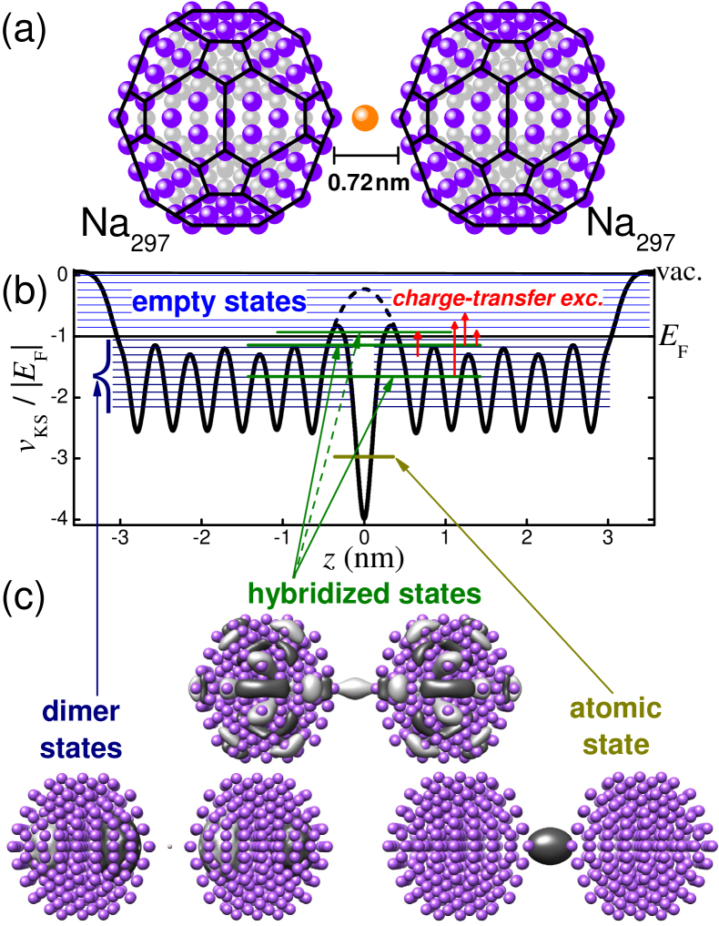
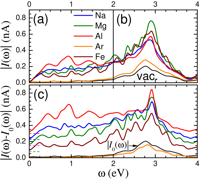
The calculated optoelectronic response is depicted in Fig. 2 and 3 for different one-atom junctions (Na, Mg, Al, Ar, and Fe) and compared to the response of the bare dimer. In line with previous jellium Zuloaga et al. (2009); Marinica et al. (2012) and ab-initio Zhang et al. (2014); Varas et al. (2015) TDDFT calculations, the optical absorption for the dimer (Fig. 2) is dominated by the so-called bonding dipolar plasmon (BDP) at , whereas a second mode, the bonding quadrupolar plasmon (BQD), appears as a less-defined spectral feature at . These plasmonic features emerge after a high renormalization of low-energy single-electron excitations due to the electron-electron (e-e) interaction Yannouleas et al. (1993); Bernadotte et al. (2013); Zhang et al. (2017). The induced AC current across the empty cavity (Fig. 3) is very weak in the low-frequency region, since it is established by excitations between bonding and antibonding dimer states below the potential barrier. However, for energies greater than the current is mainly established through excitations to unoccupied states above the potential barrier (including virtual resonant states above the vacuum level), which are strongly enhanced by the induced -field associated to a plasmon resonance.
The above picture changes dramatically for single-atom junctions. As it is schematically depicted in Fig. 1, the presence of the atom leads to a depletion of the potential barrier, as well as to the appearance of deeply-bound atomic states and occupied and unoccupied hybridized atom-dimer states. Single-electron excitations involving one of these new hybridized orbitals are much less renormalized by the e-e interaction than the ones between dimer states. As a consequence, under an independent electron picture (i.e., neglecting e-e interactions in the excitation process) those transitions can hardly be distinguished in the absorption spectrum. However, once e-e interactions are considered, the series of low-energy excitations from an occupied hybridized state to several unoccupied dimer states (or from several occupied dimer states to an unoccupied hybridized state) are not obscured anymore by nearby excitations between dimer states. Then, they become visible (not embedded in the quasi-continuum of dimer excitations) as identifiable features in the spectrum at frequencies having an oscillator strength , being the KS excitation energy (i.e., the independent-electron transition energy), the Coulomb interaction operator, and the so-called XC kernel Appel et al. (2003). That is, although these modes are not plasmonic at all, they appear in the spectrum thanks to the plasmonic response of the system. Bearing in mind the quasi-continuous DOS of the dimer states and that one atomic orbital of energy leads to several hybridized states around , once the lifetime of the excitations is accounted for, the expected outcome from each atomic orbital is a series of asymmetric Fano-like peaks. The overall structure of each series will depend on the DOS of occupied [unoccupied] dimer states if the hybridized state that is involved in the transitions is unoccupied [occupied].
These excitations are naturally associated to a net charge transfer (CT) between the clusters. For the case of an incident low-frequency E-field in resonance with a transition between the states and , the driven current across the junction is in phase with the external field, whereas its intensity is . As a consequence, the amplitude of the photoinduced density, , will follow an oscillatory behavior in the low-frequency regime resembling the one corresponding to the optical absorption. These are indeed the trends shown by the ab-initio calculations as can be seen in panels (a) of Fig. 2 and 3. Then, it is not a surprise that the changes induced by an Ar atom are negligible, whereas the optoelectronic response for the rest of the cases depends very sensitively on the atom that constitutes the junction.
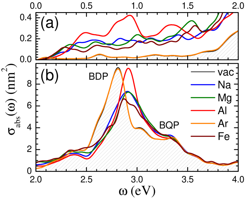
As mentioned above, this low-frequency response is mainly determined by the DOS of the system. The eigenenergies of the hybridized states can be easily extracted by direct comparison of the DOSs of the bridged- and the bare-dimer systems. For the Mg and Fe cases, the occupied s-like hybridized states lie well below the Fermi level (around 2.3 and 2.7 eV below for Mg and Fe, respectively; the Fe atomic states preserving their atomic character), whereas the unoccupied hybridized states appear for both cases around 0.3 eV above . Therefore, the CT modes correspond to transitions from occupied dimer states to unoccupied hybridized states. Since the hybridization is larger for the embedded Mg atom, the absorption is more intense in this case, but their overall spectral shape is very similar. For the Na junction, there are occupied and unoccupied 3s hybridized states around the Fermi level. Then, the optical absorption spectrum results from the superposition of two series of peaks, corresponding to transitions from [to] occupied [unoccupied] hybridized states. Finally, for Al we have several channels for the CT modes: occupied and unoccupied hybridized states close to , as well as unoccupied ones. Due to the number of channels and the efficient hybridization of the p orbitals, the optical absorption for the Al junction is more intense but less resolved.
CT modes do also contribute to the higher-frequency response, which is primarily dominated by the BDP of the dimer. Since CT excitations involve a dimer state, they will be necessarily hybridized with the renormalized single-electron excitations that constitutes the surface plasmon. For the systems considered in this Letter, a detailed quantitative analysis of such hybridizations is cumbersome. However, if atomic-chain dimers are considered instead, the plasmon is made up by only one (or a few) highly renormalized single-electron excitations Bernadotte et al. (2013). In this case, the strong hybridization of CT and plasmon modes is evident Sánchez-Barquilla et al. (2019) and the final plasmonic feature is made up by two CT excitations with a mixed “plexcitonic”character Manjavacas et al. (2011). Moreover, new CT channels involving deeper occupied hybridized states will now contribute to the response. The AC current across the junction will be then enhanced by the participation of hybridized CT modes in the plasmonic response and, to a lesser extent, by the aforementioned depletion of the potential barrier between the clusters. As a consequence, a redistribution of the spectral weight around the original BDP frequency is expected, which results on changes of the width and shape of the surface plasmon peak. In addition, due to the enhanced current between the nanoparticles, the BDP will be blueshifted Pérez-González et al. (2010).
| Atom | vac. | Na | Mg | Al | Si | P | S | Cl | Ar | Fe |
|---|---|---|---|---|---|---|---|---|---|---|
| (eV) | 2.81 | 2.91 | 2.91 | 2.92 | 2.89 | 2.88 | 2.87 | 2.85 | 2.81 | 2.88 |
| (eV) | 0.31 | 0.55 | 0.49 | 0.32 | 0.39 | 0.37 | 0.32 | 0.31 | 0.31 | 0.58 |
The above considerations perfectly explain the results depicted in panels (b) of Fig. 2 and 3 [see also Table 1, where we present the maximum and the width (FWHM) of the plasmon peak for different atomic junctions]. The inclusion of an Ar atom does not change at all the optical absorption, but the intensity of the induced current increases for eV range due to the depletion of the potential barrier. However, for the rest of the junctions there is a noticeable modification of the plasmonic response which depends on the specific atomic element. In general, the main BDP feature is blueshifted, broadened, and for the Fe case also fragmented.
This dependence plenty manifests in the behavior of the induced current. A fair estimation of the changes in the current due to the one-atom junction itself is given by , where is the intensity of the induced current for the bare dimer. As we may see in panel (c) of Fig. 3, there is a plasmon-induced strong enhancement of the CT-modes contribution to the current. Besides, for the Mg- and Fe-bridged systems there are new oscillatory features which correspond to higher-frequency series of CT excitations from occupied s-like hybridized states of the Mg and Fe atoms. In fact, for the case of Fe the hybridization of one of these CT excitations is so intense that it can be distinguished not only in the AC current spectrum but also in the optical absorption, being the main responsible of the aforementioned split of the BDP.
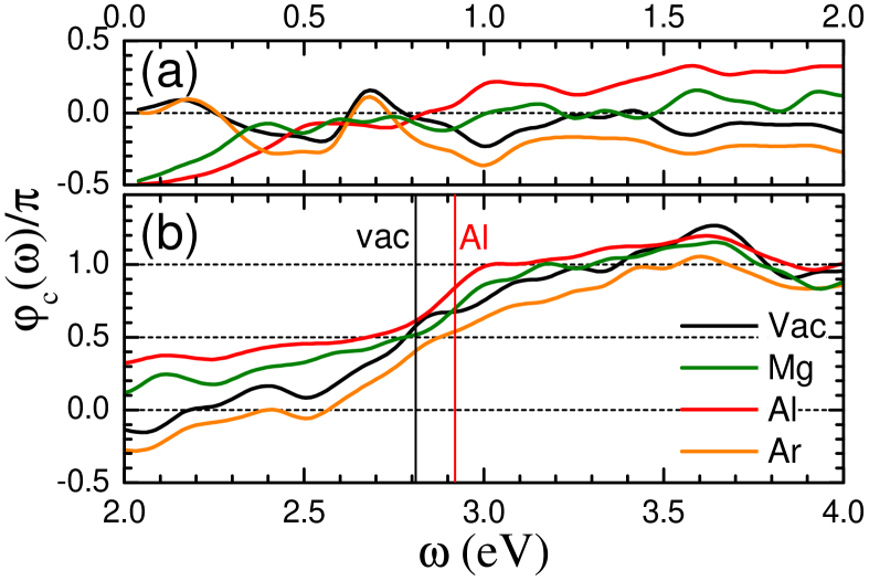
Finally, the existence of CT modes is also reflected on the AC-current phase (see Fig. 4). When such modes do not exist (as in the bare and Ar-bridged dimers), the induced current in the static limit () is in phase with the external E-field, which is the expected behavior of a “pure” tunneling regime. Then, in the low-frequency range, where the driving E-field is mainly the external one, oscillates around zero, although the center of the oscillations is shifted to negative values for higher frequencies. Since this shift is more pronunced for the Ar-bridged dimer and appears at lower frequencies than for the bare dimer, we may attribute it to the opening of new excitation channels above the potential barrier betwen the two clusters. Finally, in the “plasmonic” frequency range, where the driving E-field is mainly the induced one, the phase increases almost monotonically from , in such a way that at the BDP frequency Marinica et al. (2012); Varas et al. (2016) and at the BQP frequency.
By contrast, when the current is mainly established by excitations of CT modes (for instance, Mg- and Al-bridged dimers), in the static limit, as correponds to an out-of-resonance transition. Then, the phase increases monotonically to a value approximately equal to zero until the onset of CT excitations is reached and, eventually, it slowly increases in an oscillatory manner to a value around the bare-dimer BDP plasmon frequency . Finally, the behavior for as the frequency increases is qualiatively simlar than in the previous case. However, it is worth emphasizing that the phase at the corresponding BDP frequency is closer to than to , which is the most noticeable outcome of the existence of CT excitations in this frequency range.
In conclusion, we have elucidated and illustrated by means of ab-initio calculations the mechanisms of the optoelectronic response in hybrid systems composed by metallic plasmonic nanoparticles bridged by atomic junctions. We have shown how the changes in the optical and transport properties of the system depend strongly on the nature of the single atom junction but, unlike the DC regime in the limit of zero bias, the induced current is also affected by the overall DOS of the nanoparticles. Furthermore, the AC current can be enhanced through the hybridization of surface plasmon resonances and charge-transfer modes. Thus, the control of various parameters, such as the geometry of the nanoparticles, their separation, type of molecules constituting the junction, and also the dielectric environment, would offer us unique ways towards new molecular optoelectronic devices.
Acknowledgements.
Enlightening discussions with J. C. Cuevas, A. I. Fernández-Domínguez, and C. Tejedor are thankfully acknowledged. This work has been supported by the European Research Council (ERC-2011-AdG-290981 and ERC-2015-AdG-694097) and the Spanish Government (“María de Maeztu” Programme for Units of Excellence in R&D MDM-2014-0377 and grant MAT2014-53432-C5-5-R).References
- Ward et al. (2010) D. R. Ward, F. Hüser, F. Pauly, J. C. Cuevas, and D. Natelson, Nat. Nanotechnology 5, 732 (2010).
- Arielly et al. (2011) R. Arielly, A. Ofarim, G. Noy, and Y. Selzer, Nano Lett. 11, 2968 (2011).
- Savage et al. (2012) K. J. Savage, M. M. Hawkeye, R. Esteban, A. G. Borisov, J. Aizpurua, and J. J. Baumberg, Nature (London) 491, 574 (2012).
- Scholl et al. (2013) J. A. Scholl, A. García-Etxarri, A. L. Koh, and J. A. Dionne, Nano Lett. 13, 564 (2013).
- Hajisalem et al. (2014) G. Hajisalem, M. S. Nezami, and R. Gordon, Nano Lett. 14, 6651 (2014).
- Vadai et al. (2013) M. Vadai, N. Nachman, M. Ben-Zion, M. Barkle, F. Pauly, J. C. Cuevas, and Y. Selzer, J. Phys. Chem. Lett. 4, 2811 (2013).
- Tan et al. (2014) S. F. Tan, L. Wu, J. K. Yang, P. Bai, M. Bosman, and C. A. Nijhuis, Science 343, 1496 (2014).
- Benz et al. (2015) F. Benz, C. Tserkezis, L. O. Herrmann, B. de Nijs, A. Sanders, D. O. Sigle, L. Pukenas, S. D. Evans, J. Aizpurua, and J. J. Baumberg, Nano Lett. 15, 669 (2015).
- Lerch and Reinhard (2016) S. Lerch and B. M. Reinhard, Adv. Mater. 28, 2030 (2016).
- Sanders et al. (2016) A. Sanders, R. W. Bowman, and J. J. Baumberg, Sci. Reports 6, 22988 (2016).
- Xiang et al. (2017) D. Xiang, J. Wu, and R. Gordon, Nano Lett. 17, 2584 (2017).
- Lerch and Reinhard (2017) S. Lerch and B. M. Reinhard, Int. J. of Mod. Phys. B 31, 1740002 (2017).
- Benz et al. (2016) F. Benz, M. K. Schmidt, A. Dreismann, R. Chikkaraddy, Y. Zhang, A. Demetriadou, C. Carnegie, H. Ohadi, B. de Nijs, R. Esteban, J. Aizpurua, and J. J. Baumberg, Science 354, 726 (2016).
- Barbry et al. (2015) M. Barbry, P. Koval, F. Marchesin, R. Esteban, A. G. Borisov, J. Aizpurua, and D. Sánchez-Portal, Nano Lett. 15, 3410 (2015).
- Urbieta et al. (2018) M. Urbieta, M. Barbry, Y. Zhang, P. Koval, D. Sánchez-Portal, N. Zabala, and J. Aizpurua, ACS Nano 12, 585 (2018).
- Shin et al. (2018) H.-H. Shin, G. J. Yeon, H.-K. Choi, S.-M. Park, K. S. Lee, and Z. H. Kim, Nano Lett. 18, 262 (2018).
- Zuloaga et al. (2009) J. Zuloaga, E. Prodan, and P. Nordlander, Nano Lett. 9, 887 (2009).
- Marinica et al. (2012) D. Marinica, A. Kazansky, P. Nordlander, J. Aizpurua, and A. G. Borisov, Nano Lett. 12, 1333 (2012).
- Esteban et al. (2012) R. Esteban, A. G. Borisov, P. Nordlander, and J. Aizpurua, Nature Comm. 3, 825 (2012).
- Zhang et al. (2014) P. Zhang, J. Feist, A. Rubio, P. García-González, and F. J. García-Vidal, Phys. Rev. B 90, 161407 (2014).
- Varas et al. (2015) A. Varas, P. García-González, F. J. García-Vidal, and A. Rubio, J. Phys. Chem. Lett. 6, 1891 (2015).
- Varas et al. (2016) A. Varas, P. García-González, J. Feist, F. J. García-Vidal, and A. Rubio, Nanophotonics 5, 409 (2016).
- Galperin and Nitzan (2012) M. Galperin and A. Nitzan, Phys. Chem. Chem. Phys. 14, 9421 (2012).
- Emboras et al. (2016) A. Emboras, J. Niegemann, P. Ma, C. Haffner, A. Pedersen, M. Luisier, C. Hafner, T. Schimmel, and J. Leuthold, Nano Lett. 16, 709 (2016).
- Rossi et al. (2015) T. P. Rossi, A. Zugarramurdi, M. J. Puska, and R. M. Nieminen, Phys. Rev. Lett. 115, 236804 (2015).
- Marchesin et al. (2016) F. Marchesin, P. Koval, M. Barbry, J. Aizpurua, and D. Sánchez-Portal, ACS Photonics 3, 269 (2016).
- Song et al. (2011) P. Song, P. Nordlander, and S. Gao, J. Chem. Phys. 134, 074701 (2011).
- Song et al. (2012) P. Song, S. Meng, P. Nordlander, and S. Gao, Phys. Rev. B 86, 121410 (2012).
- Kulkarni and Manjavacas (2015) V. Kulkarni and A. Manjavacas, ACS Photonics 2, 987 (2015).
- Noya et al. (2007) E. G. Noya, J. P. Doye, D. J. Wales, and A. Aguado, Eur. Phys. J. D 43, 57 (2007).
- Kohn and Sham (1965) W. Kohn and L. J. Sham, Phys. Rev. 140, A1133 (1965).
- Troullier and Martins (1991) N. Troullier and J. L. Martins, Phys. Rev. B 43, 1993 (1991).
- Perdew et al. (1996) J. P. Perdew, K. Burke, and M. Ernzerhof, Phys. Rev. Lett. 77, 3865 (1996).
- Marques et al. (2003) M. A. L. Marques, A. Castro, G. F. Bertsch, and A. Rubio, Comp. Phys. Comm. 151, 60 (2003).
- Castro et al. (2006) A. Castro, H. Appel, M. Oliveira, C. A. Rozzi, X. Andrade, F. Lorenzen, M. A. L. Marques, E. K. U. Gross, and A. Rubio, Phys. Stat. Sol. (b) 243, 2465 (2006).
- Andrade et al. (2015) X. Andrade, D. Strubbe, U. De Giovannini, A. H. Larsen, M. Oliveira, J. Alberdi-Rodriguez, A. Varas, I. Theophilou, N. Helbig, M. Verstreate, L. Stella, F. Nogueira, A. Aspuru-Guzik, A. Castro, M. A. L. Marques, and A. Rubio, Phys. Chem. Chem. Phys. 17, 31371 (2015).
- Runge and Gross (1984) E. Runge and E. K. U. Gross, Phys. Rev. Lett. 52, 997 (1984).
- Yabana and Bertsch (1996) K. Yabana and G. F. Bertsch, Phys. Rev. B 54, 4484 (1996).
- Yannouleas et al. (1993) C. Yannouleas, E. Vigezzi, and R. A. Broglia, Phys. Rev. B 47, 9849 (1993).
- Bernadotte et al. (2013) S. Bernadotte, F. Evers, and C. R. Jacob, J. Phys. Chem. C 117, 1863 (2013).
- Zhang et al. (2017) R. Zhang, L. Bursi, J. D. Cox, Y. Cui, C. M. Krauter, A. Alabastri, A. Manjavacas, A. Calzolari, S. Corni, E. Molinari, E. A. Carter, F. J. García de Abajo, H. Zhang, and P. Nordlander, ACS Nano 11, 7321 (2017).
- Appel et al. (2003) H. Appel, E. K. U. Gross, and K. Burke, Phys. Rev. Lett. 90, 043005 (2003).
- Sánchez-Barquilla et al. (2019) M. Sánchez-Barquilla, J. Reino, and P. García-González, (unpublished) (2019).
- Manjavacas et al. (2011) A. Manjavacas, F. J. García de Abajo, and P. Nordlander, Nano Letters 11, 2318 (2011).
- Pérez-González et al. (2010) O. Pérez-González, N. Zabala, A. G. Borisov, N. J. Halas, P. Nordlander, and J. Aizpurua, Nano Lett. 10, 3090 (2010).