Ab initio Investigation of Structural Stability and Exfoliation Energies in Transition Metal Dichalcogenides based on Ti-, V-, and Mo-Group Elements
Abstract
In this work, we report an ab initio investigation based on density functional theory of the structural, energetic and electronic properties of 2D layered chalcogenides compounds based in the combination of the transition-metals (\ceTi, \ceZr, \ceHf, \ceV, \ceNb, \ceTa, \ceCr, \ceMo, \ceW and chalcogenides (\ceS, \ceSe, \ceTe) in three polymorphic phases: trigonal prismatic (2H), octahedral (1T) and distorted octahedral (1T). We determined the most stable phases for each compound, verifying the existence of the 1T phase for a small number of the compounds and we have also identified the magnetic compounds. In addition, with the determination of the exfoliation energies, we indicated the potential candidates to form one layer material and we have also found a relation between the exfoliation energy and the effective Bader charge in the metal, suggesting that when the materials present small exfoliation energy, it is due to the Coulomb repulsion between the chalcogen planes. Finally, we analyzed the electronic properties, identifying the semiconductor, semimetal and metal materials and predicting the band gap of the semiconductors. In our results, the dependence of the band gap on the -orbital is explicit. In conclusion, we have investigated the properties of stable and metastable phases for a large set of TMD materials, and our findings may be auxiliary in the synthesis of metastable phases and in the development of new TMDs applications.
I Introduction
Layered Materials have been known for years Wilson and Yoffe (1969) and are applied in areas as diverse as dry lubricants Clauss (1972), batteries Whittingham (2004), catalysts Lv et al. (2014), among others. Recently, layered transition-metal dichalcogenides (TMDs), materials with chemical formula i \ce2, with being a transition-metal and a chalcogen (\ceS, \ceSe and \ceTe), have attracted wide technological interest due to their capacity of being isolated into one layer, like graphene does Chhowalla et al. (2013); Geim and Novoselov (2007), and the wide spectrum of the electronic properties they present, being metals, semimetals, semiconductors and insulators Kolobov and Tominaga (2016). Recently, there were reported TMDs presenting exotic electronic properties, such as having topological insulator states Peng et al. (2017), being a Weyl semimetal Deng et al. (2016) and displaying charge density waves Kolobov and Tominaga (2016). The wide spectrum of properties presented by TMDs is enabled by their large number of chemical compositions combining and and the existence of several polymorphic phases Hulliger and Lévy (1977); Chhowalla et al. (2013); Kolobov and Tominaga (2016).
In TMDs, layers composed of covalently bound and planes are bound to each other by van der Waals interactions, and distinct coordination environments of the metal atoms within each layer generate structural polymorphism in these materials. Among these polymorphic phases, we highlight the most stable ones for a wide variety of materials Voiry et al. (2015); Hulliger and Lévy (1977): trigonal prismatic (2H), octahedral (1T) and distorted octahedral (1T). The lowest energy polymorph for a TMD depends mainly on the atomic radii and on the filling of the metal - orbitals Voiry et al. (2015), e.g., \ceTi group metals (\ceTi, \ceZr and \ceHf) favor 1T as the lowest energy phase Yang et al. (2017). On the other hand, the Peierls distortion mechanism is crucial for the energetic favoring of the 1T phase in some compounds, since it breaks the degeneracy of electronic states, reducing the energy Yang et al. (2017); Besse et al. (2018).
The coexistence among different phases is linked to parameters such as temperature or pressureKeum et al. (2015); Cho et al. (2015), and for the same material two different polymorphic phases may drastically change properties, e.g., \ceMoS2 in 2H and 1T phase is a semiconductor and a metal respectively Wypych and Schöllhorn (1992); Tang and en Jiang (2015). The synthesis of many polymorphic phases has been possible with the advance of experimental techniques Wong et al. (2016); Diaz et al. (2016); Loh et al. (2015); Tan et al. (2014), allowing to obtain polymorphic phases which are not at the lowest energies. However, few studies were done in these metastable phases and a comprehensive characterization of TMD compounds and polymorphs is important to explore their properties and identify stability factors.
A key factor for the renewed interest in layered TMDs is the production of two-dimensional (2D) materials from the mechanical or chemical exfoliation of the layers Novoselov et al. (2005). The easiness to exfoliate the materials comes from the weak binding between layers, which depends on the van der Waals interactions, much weaker than the in-plane covalent bonding. However, some materials are more difficult to exfoliate than others due to stronger interlayer binding and, as suggested by Monet et al. Mounet et al. (2018), the exfoliation energy can be used to determinate how easy it is to exfoliate the layers from the crystal. Previous studies report exfoliation energies only for TMDs at the lowest energy phases and studies involving another polymorphic phases are not common. Therefore, a thorough evaluation of the exfoliation energy in different TMD compounds and polymorphs is called for as an effective way to guide the production of two-dimensional materials.
To obtain a comprehensive description of the properties of layered TMDs, we performed a first-principles investigation of the stability, exfoliation energy and electronic properties of TMDs formed by \ceTi-, \ceV- and \ceCr-group transition metals and \ceS, \ceSe and \ceTe, in three different polymorphic phases: 2H, 1T, 1T’. The elastic constants of the materials were calculated, which provide means to evaluate their stability, and the magnetic order was also considered. Based on the exfoliation energies and on the analysis of charge transfer between metals and chalcogens, we identified trends correlating the intralayer charge transfer with the magnitude of interlayer binding. Lastly, we classified all the studied TMDs compositions and polymorphic phases according to their electronic properties.
II Theoretical Approach and Computational Details
Our first-principles calculations are based on the density functional theory (DFT) formalism Hohenberg and Kohn (1964); Kohn and Sham (1965) within the semi-local exchange and correlation functional proposed by Perdew–Burke–Ernzerhof (PBE) Perdew et al. (1996). The Kohn–Sham equations were solved using the PAW method Blöchl (1994) as implemented in the Vienna ab initio simulation package (VASP), version Kresse and Hafner (1993); Kresse and Furthmüller (1996). We focus on layered dichalcogenides, and it is well known from the literature that the PBE functional underestimates long range interactions such as the London dispersion Tsuneda (2014). To minimize this problem, we employed the semi-empirical DFT-D3 method proposed by Grimme et al. Grimme et al. (2010), which has been shown to provide structural properties for \ceMoS2 in good agreement with experimental results Peelaers and de Walle (2014a).
It has been well known that (semi-) local functionals fail to accurately predict band gap energies Perdew and Zunger (1981); Parr and Weitao (1994); Mori-Sánchez et al. (2008); Kim et al. (2009); Engel and Dreizler (2011); Bastos et al. (2018), and hence, to minimize this problem, the electronic properties, such as density of states (DOS) and band structures were computed using the hybrid functional proposed by Heyd–Scuseria–Ernzerhof Heyd et al. (2003, 2006) (HSE06), which contains the PBE correlation and separates the exchange term in long and short range terms by a screening function with the parameter . The short range term is composed of of exact exchange and of PBE exchange, while the long-range term is composed only by PBE exchange. We included also the relativistic effects of spin-orbit-coupling (SOC) for the valence states through the second-variational approach Koelling and Harmon (1977).
Spin-orbit coupling (SOC) effects were included for the valence states through the second-variational approachKoelling and Harmon (1977). As showed in our previous work Bastos et al. (2018), the SOC have small impact in the structural properties, hence, for volume equilibrium, relative energy stability, exfoliation energy and elastic constants calculations, the SOC was neglected. For electronic properties, such as band structures and DOS, SOC corrections were considered only in combination with the PBE functional, due to the high computational cost of the combined HSE06-SOC calculations.
Structural optimizations were performed with PBE+D3 through the minimization of the stress tensor and of the forces on every atom. We used, for the plane-waves basis set, cutoff energy of the maximum energy recommended by VASP (ENMAX parameter from POTCAR file, as described in Table I of Supplemental Material) to determine the equilibrium lattice parameters. Using the optimized structures, the elastic constants were computed using contributions from strain-stress relations for distortions in the lattice with rigid ions and ionic relaxation contributions, determined from the inversion of ionic Hessian matrix LePage and Saxe (2002); Wu et al. (2005). To achieve the convergence condition for the elastic constant we increased the cutoff energy to ENMAX. The cutoff energy employed to compute the electronic properties, i.e., DOS, band structure and Bader charge, as well as to obtain cohesive energy and exfoliation energy, was ENMAX.
For the integration in the first Brillouin zone, we employed a Monkhorst–Pack scheme Monkhorst and Pack (1976) using a k-mesh of for 2H-\ceMoS2, and meshes with same k-point density for the remaining structures, to obtain the equilibrium structure parameters. On the other hand, the k-mesh was increased in all systems, e.g. to for 2H-\ceMoS2, to compute the electronic properties. Due to the limitations of parallel calculations of elastic constants in VASP, we employed a -centered k-mesh with fixed grid of , and for 2H, 1T, and 1T structures, respectively, for all chemical compositions. More details about the computational approach are provided in the Supplemental Material.
III Crystal structures: \ce2
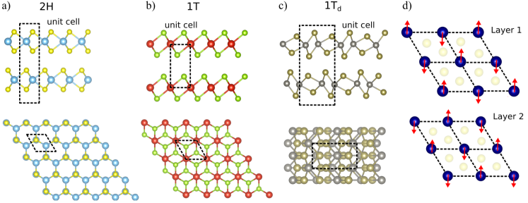
Our study concentrates on the most commonly observed TMD structural phases, 2H, 1T and 1TKolobov and Tominaga (2016). In Fig. 1, we present the schematics of the polytypes crystal structures, with 1a), 1b) and 1c) showing the top and lateral views, and 1d) indicating an example of supercell employed to access the magnetic ordering. The 2H structure, shown in 1a), is composed of a hexagonal lattice, with 2 formula units (f.u.) per unit cell, whose atoms planes are in the AbA BaB stacking sequence (capital and lower case letters for chalcogen and metal atoms planes, respectively), belonging to the space group Hulliger and Lévy (1977). The 1T structure, shown in 1b), is composed of a hexagonal lattice with 1 f.u. per unit cell, with AbCABC stacking sequence, belonging to the space group Hulliger and Lévy (1977). Each layer of the 1T structure, shown in 1c), can be generated from a 1T monolayer by reconstructions in a orthorhombic cell, originating dimerized lines of metal atoms, a distortion which has been shown to be driven by a Peierls transition mechanism Besse et al. (2018). The 1T structure is composed of an orthorhombic lattice with 4 f.u. in the unit cell, belonging to the space group. The bonding geometry symmetries correspond to , and point groups for 2H, 1T and 1T, respectively.
We address materials composed by \ceTi-, \ceV- and \ceMo-group metals, with not fully occupied -orbitals, thus some of the TMDs can exhibit non-zero magnetic moment, as has been experimentally observed in \ceVS2 and \ceVSe2 with ferromagnetic ordering in low temperatures Gao et al. (2013); Hulliger and Lévy (1977). To address the intrinsic magnetism in bulk TMDs, we employed supercells containing eight f.u., allowing to model antiferromagnetic configurations, as exemplified in Fig. 1d). For non-magnetic and ferromagnetic orderings, the unit cell was employed, since it can represent such configurations. To increase the reliability of our results, we built four antiferromagnetic initial configurations with supercells, plus the ferromagnetic one, and equilibrium volumes were obtained for every initial configuration, from which the lowest energy structure was subsequently selected. Tables with the energy comparison for the five initial configurations can be found in the Supplemental Material.
IV Results
IV.1 Relative energy stability
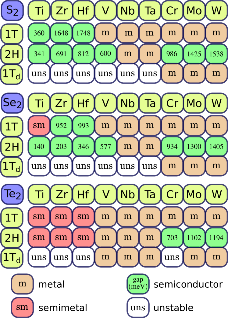
We obtained the equilibrium geometric configurations for all compounds and analyzed the relative stability between the phases (2H, 1T, 1T) by comparison of the total energy, Fig. 2. For \ceTi group compounds, \ceV group selenides and tellurides, and \ceCrTe2, the 1T phase does not present a local minimum structure in the potential surface, i.e., even if the structural relaxation starts from the 1T structure, it yields the structural configuration of the 1T phase. Therefore, these compounds are not stable in the 1T phase and these structures were not further considered in our calculations.
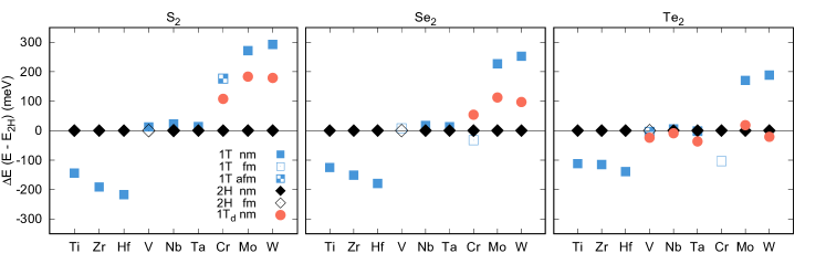
Figure 2 shows the relative total energies obtained for the three polymorphic phases using 2H phase as the reference. For all the \ceTi group compounds (\ceTi, \ceZr and \ceHf combined with \ceS,\ceSe and \ceTe) the lowest energy phase is 1T, as expected Chhowalla et al. (2013), while for the \ceV and \ceCr groups compounds there is an alternation of the lowest energy phase. The \ceV group compounds have a small energy difference between the phases, which is manifested with the synthesis of 2H and 1T phases among these materials Kolobov and Tominaga (2016), and 2H is the most stable for compounds with \ceS and \ceSe whereas 1T is the most stable for compounds with \ceTe. Compounds with \ceV are experimentally observed in the 2H phase, in contrast with our results, however it has been shown that due to the small energy difference between the phases, temperature effects might change the lowest energy phase, in agreement with the synthesis of 1T-\ceVS2 at room temperatureZhang et al. (2013).
In \ceCr group, 2H predominates as the lowest energy phase (\ceMo2, \ceWS2, \ceWSe2), as expected Chhowalla et al. (2013). The exceptions are \ceCrSe2 (1T), \ceCrTe2 (1T), and \ceWTe2 (1T), which were all experimentally observed crystal structures Freitas et al. (2013, 2015); Kolobov and Tominaga (2016). Finally, the room temperature crystal structures of \ceNbTe2 and \ceTaTe2, which are formed of a monoclinic lattice Brown (1966), are not considered in our calculations. However, among the structures considered, the 1T phase, that has the same intra-layer structural configuration of distorted octahedral coordination of metal atoms, was obtained as the lowest energy one for these compounds.
Therefore, our results are in line with the general rule of the strong influence of the filling of metal orbitals on the lowest energy phase of each compound Chhowalla et al. (2013); Yang et al. (2017), as can be seen in the preference of 1T phase for \ceTi group compounds, and mostly 2H phase for TMDs of \ceV and \ceCr groups. However, other effects are important to determine the energetic favored phase, like magnetism. From our results, only the \ceV group and \ceCr compounds favor a magnetic ordering, depending on the phase: \ceVS2, \ceVSe2, \ceVTe2 and \ceNbS2 in 2H phase are ferromagnetic, as well as \ceVSe2 and \ceTaTe2 in 1T phase, while \ceCrS2 and \ceVTe2 in 1T phase are antiferromagnetic. This information is also presented in Fig. 2. A recent theoretical work Mounet et al. (2018) reported that the 1T monolayers of \ceV dichalcogenides are ferromagnetic, and 1T-\ceCrSe2 monolayer is reported as antiferromagnetic.
The antiferromagnetic ordering was also obtained by experimental measurements in bulk 1T-\ceCrSe2Freitas et al. (2013), although we obtained lower energy for the ferromagnetic ordering. The energy difference between the two orderings in our calculations, however, is of only , i.e., the phases are approximately degenerate and stable. Furthermore, this difference is so small that, the use of a different vdW correction may change the result, also considering that variations on the lattice parameter were shown to modify the energetic preference between the two orderingsFreitas et al. (2013). The relative energies for all magnetic configurations are presented in the Supplemental Material.
IV.2 Exfoliation energy
To investigate the strength of interlayer binding in TMDs and determine how easily they can be exfoliated, we calculated the exfoliation energy. As the polymorphic structures have different unit cells, we calculate exfoliation energies per monolayer area in the unit cell. In Fig. 3, the exfoliation energy is shown as a function of metal effective Bader charge Bader (1994); Tang et al. (2009), i.e., an estimate of the charge transfer from metal to chalcogen atoms. Several works, using different levels of vdW corrections Björkman et al. (2012a, b); Choudhary et al. (2017); Ashton et al. (2017); Mounet et al. (2018), propose a classification of the materials that are easily or potentially exfoliable based on the exfoliation energy. We adopt the classification in which materials with exfoliation energy of are considered easily exfoliable, while materials with energies above these values up to are considered potentially exfoliable.
In our results, almost all the studied compounds have exfoliation energy in the range of and can be classified as easily exfoliable, as shown in Fig. 3. The exceptions are: \ceCrSe2 and \ceCrTe2 in the 1T phase, with , respectively; \ceVTe2, \ceTaTe2 and \ceNbTe2 in the 1T phase, with , respectively.
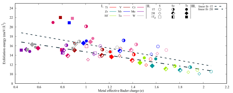
An analysis of Fig. 3, shows that the exfoliation energy decreases linearly with the increase of the metal effective Bader charge, presenting a clear trend. This relation arises because with the increase of the charge on metal atoms, and consequently increase of the magnitude of the charge on the chalcogen plane, the effective Coulomb repulsion among the layers also increases, resulting in larger interlayer distances and smaller exfoliation energy. There is a small difference between polymorphic phases, as indicated by the separate linear fittings in Fig. 3, which may be related to the atom ordering in the chalcogen plane. As generally 1T phase has higher in-plane lattice parameters when compared with 2H, less charge is accumulated in the chalcogen plane in 1T than in 2H. As a result, the distance between planes is smaller and the exfoliation energy is larger. Nevertheless, this difference is small, as shown for 2H and 1T \ceZrS2 in Fig. 3. When the charge transfer is lower, Coulomb repulsion plays a smaller role, leading the exfoliation energies to be more dependent on other effects, e.g. van der Waals interaction, causing larger deviations from the linear trend, as with the cases of stronger () interlayer binding. Thus, the linear correlation is not clear for 1T, which may be due to the non-uniformities in the chalcogen plane caused by the distortions typical of this phase. All values of exfoliation energy and Bader charge are available in Supplemental Material.
IV.3 Equilibrium volume
In Fig. 4, we show in-plane, , and perpendicular, , lattice parameters. Due to the different number of layers in the unit cells between the polymorphs, in order to compare all the materials, we used the value of the out-of-plane lattice parameter divided by the number of layers to obtain . As expected, the lattice parameters increase monotonically with the chalcogen atomic radius (covalent radius reference values are for \ceS, \ceSe, \ceTe respectivelyKittel (1996)), as shown in Fig. 4 a),d). The exceptions are the 1T \ceCr compounds that present an abnormal increase of from \ceCrSe2 to \ceCrS2.
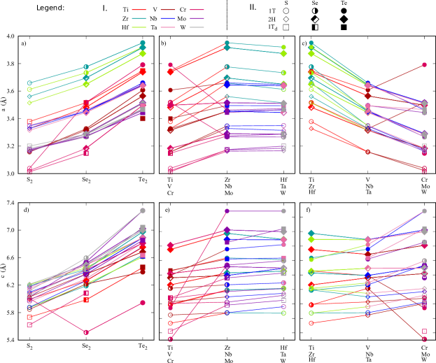
The effect of varying transition-metal period, with fixed metal group and chalcogen species, on the lattice parameters is represented in Fig. 4 b), e). Compounds with transition-metal belonging to period (\ceTi, \ceV and \ceCr) have the smallest parameters, while compounds with transition metals belonging to periods (\ceZr, \ceNb and \ceMo) and (\ceHf, \ceTa and \ceW) have similar lattice parameters. This is also in agreement with the trend of atomic radii of the transition metals, which are the smallest for transition metals belonging to period and have close values for transition metals from periods and , for example for \ceCr, \ceMo and \ceW, respectively Kittel (1996).
| phase | phase | phase | |||||||||||||||
| \ceTiS2 | 2H | DFT | \ceTiSe2 | 2H | DFT | \ceTiTe2 | 2H | DFT | |||||||||
| 1T | 1T | 1T | |||||||||||||||
| 1T | unstable | 1T | unstable | 1T | unstable | ||||||||||||
| 1T | Exp. | 1T | Exp. | 1T | Exp. | ||||||||||||
| \ceZrS2 | 2H | DFT | \ceZrSe2 | 2H | DFT | \ceZrTe2 | 2H | DFT | |||||||||
| 1T | 1T | 1T | |||||||||||||||
| 1T | unstable | 1T | unstable | 1T | unstable | ||||||||||||
| 1T | Exp. | 1T | Exp. | 1T | Exp. | ||||||||||||
| \ceHfS2 | 2H | DFT | \ceHfSe2 | 2H | DFT | \ceHfTe2 | 2H | DFT | |||||||||
| 1T | 1T | 1T | |||||||||||||||
| 1T | unstable | 1T | unstable | 1T | unstable | ||||||||||||
| 2H | Exp. | 2H | Exp. | 2H | Exp. | ||||||||||||
| 1T | 1T | 1T | |||||||||||||||
| \ceVS2 | 2H | DFT | \ceVSe2 | 2H | DFT | \ceVTe2 | 2H | DFT | |||||||||
| 1T | 1T | 1T | |||||||||||||||
| 1T | unstable | 1T | unstable | 1T | |||||||||||||
| 1T | Exp. | 1T | Exp. | 1T | Exp. | ||||||||||||
| \ceNbS2 | 2H | DFT | \ceNbSe2 | 2H | DFT | \ceNbTe2 | 2H | DFT | |||||||||
| 1T | 1T | 1T | |||||||||||||||
| 1T | unstable | 1T | unstable | 1T | |||||||||||||
| 2H | Exp. | 2H | Exp. | 2H | Exp. | ||||||||||||
| 1T | 1T | 1T | |||||||||||||||
| \ceTaS2 | 2H | DFT | \ceTaSe2 | 2H | DFT | \ceTaTe2 | 2H | DFT | |||||||||
| 1T | 1T | 1T | |||||||||||||||
| 1T | unstable | 1T | unstable | 1T | |||||||||||||
| 2H | Exp. | 2H | Exp. | 2H | Exp. | ||||||||||||
| 1T | 1T | 1T | |||||||||||||||
| \ceCrS2 | 2H | DFT | \ceCrSe2 | 2H | DFT | \ceCrTe2 | 2H | DFT | |||||||||
| 1T | 1T | 1T | |||||||||||||||
| 1T | 1T | 1T | unstable | ||||||||||||||
| \ceMoS2 | 2H | DFT | \ceMoSe2 | 2H | DFT | \ceMoTe2 | 2H | DFT | |||||||||
| 1T | 1T | 1T | |||||||||||||||
| 1T | 1T | 1T | |||||||||||||||
| 2H | Exp. | 2H | Exp. | 2H | Exp. | ||||||||||||
| \ceWS2 | 2H | DFT | \ceWSe2 | 2H | DFT | \ceWTe2 | 2H | DFT | |||||||||
| 1T | 1T | 1T | |||||||||||||||
| 1T | 1T | 1T | |||||||||||||||
| 2H | Exp. | 2H | Exp. | 1T | Exp. | ||||||||||||
The atomic radii of transition metals (e.g., , and for \ceTi, \ceV and \ceCr, respectively Kittel (1996)) also determine the decrease of the parameter with the increase of the column number of the transition metal group, for a fixed period and a chalcogen species, as shown in Fig. 4c). There is no clearly defined trend for the parameter. Compared with the experimental data for the already synthesized TMDs, as showed in the Table 1, the calculated lattice parameters present mean absolute percentage errors (MAPE) lower than for in-plane lattice parameters ( and ) and lower than for the perpendicular lattice parameter (), indicating that PBE-D3 predicts reasonable values for VdW effects in TMDs.
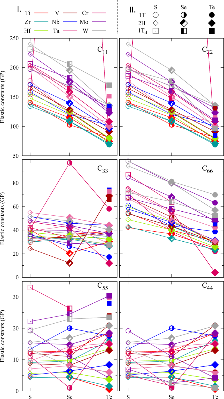
IV.4 Elastic constants
As we consider some compositions and polymorphic phases not yet synthesized, the structural stability of the materials was addressed by the Born elastic stability criteria Born and Huang (1998), and hence, we analyzed the stability of the TMDs through the evaluation of the elastic constants and verification of the Born elastic stability criteria as discussed by Mouhat and Coudert Mouhat and Coudert (2014). Due to their symmetry, the crystals of 1T, 2H and 1T phases present , and non-zero and independent elastic constants, respectively, which must satisfy the necessary and sufficient conditions for stability discussed below.
For the 1T phase ( space group), with elastic constants , , , , and (and ), the conditions are:
| (1) |
For the crystal of 2H phase ( space group), that has the elastic constants , , , , (with ), the conditions are:
| (2) |
Finally, the elastic constants of the 1T phase crystal ( space group), , , , , , , , and , must satisfy the following conditions:
| (3) |
All the elastics constants values are shown in the Supplemental Material, while the diagonal elastic constants are shown in Fig. 5. We found that all conditions for the elastic stability are satisfied, and hence, those configurations are local minimum structures. Our results are in agreement with previous calculations Peelaers and de Walle (2014b) and experimental results Kolobov and Tominaga (2016); Feldman (1976). For the elastic constants and , which are not related to the out of plane direction (), the magnitude decreases with the chalcogen radius and have higher values when compared with the other elastic constants, as shown in Fig. 5. This occurs because in plane binding, that is dominated by covalent bonds, is weaker for larger chalcogen radius, and is stronger than the out of plane van der Waals interactions. Therefore, the other elastic constants, which are related to the direction, have a smaller magnitude, and present deviant trends for the chalcogen radius, due to the role of the van der Waals interactions in the interlayer interactions.
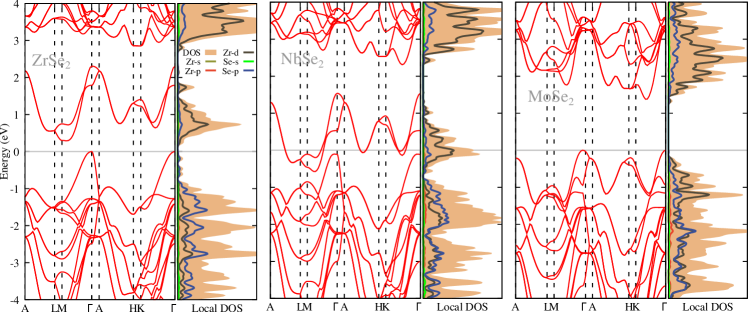
IV.5 Band structure and density of states
To characterize the materials according to their electronic properties, we calculated the band structure and the density of states of the stable TMDs with the hybrid functional HSE06. The results for 2H-phase selenides of the -metals are shown in Fig. 6, and the results for the other systems are in the Supplemental Material. From the analysis of the results, the materials were classified as metals, semi-metals or semiconductors, as indicated in Fig. 7. Among all the studied TMDs, were identified as semiconductors, with band gaps ranging from .
In the literature, works that estimate the band gaps for TMDs in the bulk phase mainly use the crystal structures acquired from crystallographic databases Lebègue et al. (2013); Zhu et al. (2018) presenting band gap values that differ from our results. The difference of values is due to the use of the PBE functional, that is known to underestimate the band gap Perdew and Zunger (1981); Bastos et al. (2016, 2018). In Table IV.5, we present the values of PBE, PBE+SOC, HSE06 and experimental band gaps for the TMD semiconductor materials. The comparison of PBE and PBE+SOC shows that the inclusion of SOC modify the gap values usually from less than one to a few decades of , exception made for \ceZrSe2-1T, \ceHfSe2-1T and \ceWTe2-2H where this difference is about 150 . However, the PBE functional usually underestimates the gap in the order of several hundreds of s. Despite the absence of the SOC corrections on the HSE06 calculations this functional shows more realistic band gaps when compared with the experimentally measured values, preventing the high computational costs associated to the combined use of HSE06 and SOC.
For each phase and considering compositions with the same chalcogen, the transition metal electron count determines the electronic character of the material. For example, in 2H-\ceSe compounds, as shown in Fig. 6, with the progressive filling of the band from \ceZr to \ceNb to \ceMo \ceZrSe2 is a semiconductor, while \ceNbSe2 is a metal, and the band is fully occupied in \ceMoSe2, recovering the semiconductor character. Therefore, if the -orbitals are completely occupied or empty, the TMDs have semiconducting behavior, while if the -orbitals have the partial occupation, the TMDs have conducting behavior. These results are in agreement with other reports in the literature Yang et al. (2017); Voiry et al. (2015). Because the crystal symmetry, i.e. the polymorphic phase, strongly affects the energy of the bands, the same compound can have different electronic properties depending on the polymorphic phase. For example, \ceMoS2 is metallic in the 1T phase, but is a semiconductor in the 2H phaseWypych and Schöllhorn (1992); Tang and en Jiang (2015).
Band gaps vary with the composition in a similar way for the three studied phases. The increase in chalcogen atomic number narrows the band gap, because the energy of - derived states, which compose the valence band maximum, is increased. For semiconductors with the same phase and chalcogen, the band gap increases with the transition metal atomic number, e.g., \ceTiQ2\ceZrQ2\ceHfQ2gap in phase 1T, as shown in Fig. 7. This trend occurs due to the localization of the orbitals, since their energy difference from the Fermi energy increases, i.e., looking for compounds with the same phase, the -orbitals in \ceTiS2 have energies closer to Fermi energy than those in \ceZrS2.
PBE, PBE with spin-orbit coupling (PBE+SOC), HSE06 and experimental band gaps for TMD semiconductor materials. All energies are given in . Material Phase PBE PBE+SOC HSE06 Exp. \ceTiS2 1T \ceZrS2 1T \ceZrSe2 1T \ceHfS2 1T \ceHfSe2 1T \ceTiS2 2H \ceTiSe2 2H \ceZrS2 2H \ceZrSe2 2H \ceHfS2 2H \ceHfSe2 2H \ceVS2 2H \ceVSe2 2H \ceCrS2 2H \ceCrSe2 2H \ceCrTe2 2H \ceMoS2 2H 1230b \ceMoSe2 2H 1090b \ceMoTe2 2H 880a \ceWS2 2H 1350b \ceWSe2 2H 1200b \ceWTe2 2H
V Conclusion
We investigated TMD bulk compounds obtained by the combination of nine transition-metals (\ceTi, \ceZr, \ceHf, \ceV, \ceNb, \ceTa, \ceCr, \ceMo and \ceW) with three chalcogens (\ceS, \ceSe and \ceTe) in three polymorphic phases, namely, 1T, 2H, and 1T. We obtained the equilibrium geometry configuration and the lowest energy phase for each material, which are in good agreement with experimental data for the already synthesized compositions. The magnetic ordering was also addressed, and some of the materials with transition-metal from the \ceV group and compounds with \ceCr showed ferromagnetic or antiferromagnetic behavior. The effects of chemical composition on the equilibrium lattice parameters mostly follow the expected trends based on the atomic radius.
To investigate the stability of the crystal structures, we obtained the elastic constants and employed the Born elastic stability criteria, which was satisfied for all the systems. The exfoliation energy of all stable materials was calculated, indicating that the majority of the studied TMDs have weak interlayer binding and therefore are predicted as easy to exfoliate in order to obtain their two-dimensional form. We found that the increase of the charge transfer within each layer decreases the magnitude of the exfoliation energy, due to the Coulomb repulsion between chalcogen planes. The electronic band structure and density of states were calculated, which allowed classifying the materials like metal, semimetal or semiconductor, according to their band gap. We demonstrated that the occupation of metal band determines the electronic character of the material. This study provides a comprehensible understanding of the properties of layered TMDs in different polymorphic phases, including material not yet synthesized, and therefore can contribute to further development of layered and two-dimensional materials based on TMDs.
VI Acknowledgments
The authors gratefully acknowledge support from FAPESP (São Paulo Research Foundation, Grant Number 2017/11631-2), Shell and the strategic importance of the support given by ANP (Brazil’s National Oil, Natural Gas and Biofuels Agency) through the R&D levy regulation. R.B. acknowledges financial support (Ph.D. fellowship) from FAPESP, Grant No. 2017/09077-7. This study was financed in part by the Coordenação de Aperfeiçoamento de Pessoal de Nível Superior - Brasil (CAPES) - Finance Code 001. G.M.S. acknowledges CAPES-CsF (grant No. 88881.068174/2014-01) and CNPq (grants No. 304289/2015-9 and 308806/2018-2).
References
- Wilson and Yoffe (1969) J. Wilson and A. Yoffe, Adv. Phys. 18, 193 (1969).
- Clauss (1972) F. J. Clauss, Solid Lubricants and Self-Lubricating Solids (Elsevier, 1972).
- Whittingham (2004) M. S. Whittingham, Chem. Rev. 104, 4271 (2004).
- Lv et al. (2014) R. Lv, J. A. Robinson, R. E. Schaak, D. Sun, Y. Sun, T. E. Mallouk, and M. Terrones, Acc. Chem. Res. 48, 56 (2014).
- Chhowalla et al. (2013) M. Chhowalla, H. S. Shin, G. Eda, L.-J. Li, K. P. Loh, and H. Zhang, Nat. Chem. 5, 263 (2013).
- Geim and Novoselov (2007) A. K. Geim and K. S. Novoselov, Nat. Mater. 6, 183 (2007).
- Kolobov and Tominaga (2016) A. V. Kolobov and J. Tominaga, Two-Dimensional Transition-Metal Dichalcogenides (Springer International Publishing, 2016).
- Peng et al. (2017) L. Peng, Y. Yuan, G. Li, X. Yang, J.-J. Xian, C.-J. Yi, Y.-G. Shi, and Y.-S. Fu, Nat. Commun. 8, 65 (2017).
- Deng et al. (2016) K. Deng, G. Wan, P. Deng, K. Zhang, S. Ding, E. Wang, M. Yan, H. Huang, H. Zhang, Z. Xu, J. Denlinger, A. Fedorov, H. Yang, W. Duan, H. Yao, Y. Wu, S. Fan, H. Zhang, X. Chen, and S. Zhou, Nat. Phys. 12, 1105 (2016).
- Hulliger and Lévy (1977) F. Hulliger and F. Lévy, Structural Chemistry of Layer-Type Phases, 1st ed., Physics and Chemistry of Materials with Layered Structures 5 (Springer Netherlands, 1977).
- Voiry et al. (2015) D. Voiry, A. Mohite, and M. Chhowalla, Chem. Soc. Rev. 44, 2702 (2015).
- Yang et al. (2017) H. Yang, S. W. Kim, M. Chhowalla, and Y. H. Lee, Nat. Phys. 13, 931 (2017).
- Besse et al. (2018) R. Besse, N. A. M. S. Caturello, C. M. O. Bastos, D. Guedes-Sobrinho, M. P. Lima, G. M. Sipahi, and J. L. F. D. Silva, J. Phys. Chem. C 122, 20483 (2018).
- Keum et al. (2015) D. H. Keum, S. Cho, J. H. Kim, D.-H. Choe, H.-J. Sung, M. Kan, H. Kang, J.-Y. Hwang, S. W. Kim, H. Yang, K. J. Chang, and Y. H. Lee, Nat. Phys. 11, 482 (2015).
- Cho et al. (2015) S. Cho, S. Kim, J. H. Kim, J. Zhao, J. Seok, D. H. Keum, J. Baik, D.-H. Choe, K. J. Chang, K. Suenaga, S. W. Kim, Y. H. Lee, and H. Yang, Science 349, 625 (2015).
- Wypych and Schöllhorn (1992) F. Wypych and R. Schöllhorn, J. Chem. Soc., Chem. Commun. 0, 1386 (1992).
- Tang and en Jiang (2015) Q. Tang and D. en Jiang, Chem. Mater. 27, 3743 (2015).
- Wong et al. (2016) S. L. Wong, H. Liu, and D. Chi, Prog. Cryst. Growth Charact. Mater. 62, 9 (2016).
- Diaz et al. (2016) H. C. Diaz, Y. Ma, R. Chaghi, and M. Batzill, Appl. Phys. Lett. 108, 191606 (2016).
- Loh et al. (2015) T. A. J. Loh, D. H. C. Chua, and A. T. S. Wee, Sci. Rep. 5, 18116 (2015).
- Tan et al. (2014) L. K. Tan, B. Liu, J. H. Teng, S. Guo, H. Y. Low, and K. P. Loh, Nanoscale 6, 10584 (2014).
- Novoselov et al. (2005) K. S. Novoselov, D. Jiang, F. Schedin, T. J. Booth, V. V. Khotkevich, S. V. Morozov, and A. K. Geim, Proc. Natl. Acad. Sci. U. S. A. 102, 10451 (2005).
- Mounet et al. (2018) N. Mounet, M. Gibertini, P. Schwaller, D. Campi, A. Merkys, A. Marrazzo, T. Sohier, I. E. Castelli, A. Cepellotti, G. Pizzi, and N. Marzari, Nat. Nanotechnol. 13, 246 (2018).
- Hohenberg and Kohn (1964) P. Hohenberg and W. Kohn, Phys. Rev. 136, B864 (1964).
- Kohn and Sham (1965) W. Kohn and L. J. Sham, Phys. Rev. 140, A1133 (1965).
- Perdew et al. (1996) J. P. Perdew, K. Burke, and M. Ernzerhof, Phys. Rev. Lett. 77, 3865 (1996).
- Blöchl (1994) P. E. Blöchl, Phys. Rev. B 50, 17953 (1994).
- Kresse and Hafner (1993) G. Kresse and J. Hafner, Phys. Rev. B 48, 13115 (1993).
- Kresse and Furthmüller (1996) G. Kresse and J. Furthmüller, Phys. Rev. B 54, 11169 (1996).
- Tsuneda (2014) T. Tsuneda, Density Functional Theory in Quantum Chemistry (Springer Nature, 2014).
- Grimme et al. (2010) S. Grimme, J. Antony, S. Ehrlich, and H. Krieg, J. Chem. Phys. 132, 154104 (2010).
- Peelaers and de Walle (2014a) H. Peelaers and C. G. V. de Walle, J. Phys.: Condens. Matter 26, 305502 (2014a).
- Perdew and Zunger (1981) J. P. Perdew and A. Zunger, Phys. Rev. B 23, 5048 (1981).
- Parr and Weitao (1994) R. G. Parr and Y. Weitao, Density-Functional Theory of Atoms and Molecules (International Series of Monographs on Chemistry) (Oxford University Press, 1994).
- Mori-Sánchez et al. (2008) P. Mori-Sánchez, A. J. Cohen, and W. Yang, Phys. Rev. Lett. 100, 146401 (2008).
- Kim et al. (2009) Y.-S. Kim, K. Hummer, and G. Kresse, Phys. Rev. B 80, 035203 (2009).
- Engel and Dreizler (2011) E. Engel and R. M. Dreizler, Density Functional Theory (Springer Berlin Heidelberg, 2011).
- Bastos et al. (2018) C. M. O. Bastos, F. P. Sabino, G. M. Sipahi, and J. L. F. D. Silva, J. Appl. Phys. 123, 065702 (2018).
- Heyd et al. (2003) J. Heyd, G. E. Scuseria, and M. Ernzerhof, J. Chem. Phys. 118, 8207 (2003).
- Heyd et al. (2006) J. Heyd, G. E. Scuseria, and M. Ernzerhof, J. Chem. Phys. 124, 219906 (2006).
- Koelling and Harmon (1977) D. D. Koelling and B. N. Harmon, J. Phys. C: Solid State Phys. 10, 3107 (1977).
- LePage and Saxe (2002) Y. LePage and P. Saxe, Phys. Rev. B 65, 104104 (2002).
- Wu et al. (2005) X. Wu, D. Vanderbilt, and D. R. Hamann, Phys. Rev. B 72, 035105 (2005).
- Monkhorst and Pack (1976) H. J. Monkhorst and J. D. Pack, Phys. Rev. B 13, 5188 (1976).
- Gao et al. (2013) D. Gao, Q. Xue, X. Mao, W. Wang, Q. Xu, and D. Xue, J. Mater. Chem. 1, 5909 (2013).
- Zhang et al. (2013) H. Zhang, L.-M. Liu, and W.-M. Lau, J. Mater. Chem. A 1, 10821 (2013).
- Freitas et al. (2013) D. C. Freitas, M. Núñez, P. Strobel, A. Sulpice, R. Weht, A. A. Aligia, and M. Núñez-Regueiro, Phys. Rev. B 87, 014420 (2013).
- Freitas et al. (2015) D. C. Freitas, R. Weht, A. Sulpice, G. Remenyi, P. Strobel, F. Gay, J. Marcus, and M. Núñez-Regueiro, J. Phys.: Condens. Matter 27, 176002 (2015).
- Brown (1966) B. E. Brown, Acta Crystallogr. 20, 264 (1966).
- Bader (1994) R. F. W. Bader, Atoms in Molecules: A Quantum Theory, International Ser. of Monogr. on Chem (Clarendon Press, 1994).
- Tang et al. (2009) W. Tang, E. Sanville, , and G. Henkelman, J. Phys.: Condens. Matter 21, 084204 (2009).
- Björkman et al. (2012a) T. Björkman, A. Gulans, A. V. Krasheninnikov, and R. M. Nieminen, Phys. Rev. Lett. 108, 235502 (2012a).
- Björkman et al. (2012b) T. Björkman, A. Gulans, A. V. Krasheninnikov, and R. M. Nieminen, J. Phys.: Condens. Matter 24, 424218 (2012b).
- Choudhary et al. (2017) K. Choudhary, I. Kalish, R. Beams, and F. Tavazza, Sci. Rep. 7, 5179 (2017).
- Ashton et al. (2017) M. Ashton, J. Paul, S. B. Sinnott, and R. G. Hennig, Phys. Rev. Lett. 118, 106101 (2017).
- Kittel (1996) C. Kittel, Introduction to Solid State Physics, 7th ed. (John Wiley & Sons, New York, 1996).
- Born and Huang (1998) M. Born and K. Huang, Dynamical Theory of Crystal Lattices (Oxford Classic Texts in the Physical Sciences) (Clarendon Press, 1998).
- Mouhat and Coudert (2014) F. Mouhat and F.-X. Coudert, Phys. Rev. B 90, 224104 (2014).
- Peelaers and de Walle (2014b) H. Peelaers and C. G. V. de Walle, J. Phys. Chem.C 118, 12073 (2014b).
- Feldman (1976) J. Feldman, J. Phys. C: Solid State Phys. 37, 1141 (1976).
- Lebègue et al. (2013) S. Lebègue, T. Björkman, M. Klintenberg, R. M. Nieminen, and O. Eriksson, Phys. Rev. X 3, 031002 (2013).
- Zhu et al. (2018) Y. Zhu, X. Kong, T. D. Rhone, and H. Guo, Phys. Rev. Materials 2, 081001 (2018).
- Bastos et al. (2016) C. M. O. Bastos, F. P. Sabino, P. E. F. Junior, T. Campos, J. L. F. D. Silva, and G. M. Sipahi, Semicond. Sci. Technol. 31, 105002 (2016).
- Lezama et al. (2014) I. G. Lezama, A. Ubaldini, M. Longobardi, E. Giannini, C. Renner, A. B. Kuzmenko, and A. F. Morpurgo, 2D Mater. 1, 021002 (2014).
- Kam and Parkinson (1982) K. K. Kam and B. A. Parkinson, J. Phys. Chem. 86, 463 (1982).