M. Pflüger et al.: Distortion analysis of crystalline and locally quasicrystalline 2D photonic structures with GISAXS \sidecaptionvposfiguret
Distortion analysis of crystalline and locally quasicrystalline 2D photonic structures with GISAXS
Abstract
In this study, grazing incidence small-angle X-ray scattering (GISAXS) is used to collect statistical information on dimensional parameters in an area of on photonic structures produced by nanoimprint lithography. The photonic structures are composed of crystalline and locally quasicrystalline two-dimensional patterns with structure sizes between about and to enable broadband visible light absorption for use in solar energy harvesting. These first GISAXS measurements on locally quasicrystalline samples demonstrate that GISAXS is capable of showing the locally quasicrystalline nature of the samples while at the same time revealing the long-range periodicity introduced due to the lattice design. We describe the scattering qualitatively in the framework of the distorted wave Born approximation using a hierarchical model mirroring the sample design, which consists of a rectangular and locally quasicrystalline supercell which is repeated periodically to fill the whole surface.
The nanoimprinted samples are compared to a sample manufactured using electron beam lithography and the distortions of the periodic and locally quasiperiodic samples are quantified statistically. Due to the high sensitivity of GISAXS to deviations from the perfect lattice, the misalignment of the crystallographic axes was measured with a resolution of , showing distortions up to in the investigated samples.
1 Introduction
Grazing incidence small-angle X-ray scattering (GISAXS) is a powerful non-destructive technique for the investigation of nanostructured surfaces Renaud et al. [2009], Hexemer and Müller-Buschbaum [2015]. It has been used, for example, to measure the morphology of active layers in organic photovoltaics Gu et al. [2012], Müller-Buschbaum [2014, 2016], the defects in photonic crystals Zhou et al. [2012], interface roughness of layered systems Holý et al. [1993], Babonneau et al. [2009] and lithographically produced nanostructures Jones et al. [2003], Soccio et al. [2014], Soltwisch et al. [2017], Hagihara et al. [2017]. Local measurement techniques like scanning probe microscopy (e.g. scanning electron microscopy and atomic force microscopy) offer nanometre resolution and detailed insights into the investigated nanostructures, but only measure comparatively small areas (). Collecting statistical information on large nanostructured surfaces is therefore prohibitively time-consuming. In contrast, visible light microscopy, scatterometry and spectroscopy can quickly measure large areas, but do not easily offer nanometre resolution. Bridging this gap, GISAXS provides statistical information on the dimensional properties over the whole measurement area of about with nanometre resolution. This enables the investigation of imperfections in otherwise highly ordered lithographically produced nanostructures Rueda et al. [2012], Soccio et al. [2014], Soltwisch et al. [2016], Suh et al. [2016] even for buried structures Gann et al. [2014] as well as the investigation of the increasing disorder in nanostructures during annealing Meier et al. [2012]. However, GISAXS as a scattering technique does not offer direct imaging which necessitates rather complex data analysis and interpretation.
In this study, we use nanoimprint lithography, and for comparison electron beam lithography, to manufacture periodic and locally quasiperiodic two-dimensional photonic structures intended for use in the solar spectrum, and investigate the samples using GISAXS. To minimize the resource and energy usage of silicon photovoltaics, it is desirable to use thin active silicon films. In order to maintain high efficiency in thin-film devices, the active film is structured over the whole device surface with a structure size ranging from about to , enhancing the absorbance using light trapping or wave-optics effects Becker et al. [2013], Priolo et al. [2014]. In the finished device, the structured interface is buried under other layers (the active film, front contact or coating layers) Eisenhauer et al. [2015], which makes it difficult to measure. Here, GISAXS provides an attractive measurement technique due to the possibility to vary the depth sensitivity using different incident angles and incident photon energies Jiang et al. [2011], Wernecke et al. [2014b].
Local quasicrystallinity provides a structuring approach which leads to broadband high absorption Xavier et al. [2014, 2016]. Quasicrystals are ordered, non-periodic structures with an essentially sharp diffraction pattern, which often exhibits non-crystallographic rotational symmetry Shechtman et al. [1984], IUCr [2018]. The Fourier spectrum of quasiperiodic lattices is dense, but the Fourier components are sharp and differ in intensity, so that the scattering image shows sharp diffraction orders Suck et al. [2002]. We use the term locally quasicrystalline to describe structures satisfying the following conditions. Firstly, they must exhibit an essentially sharp diffraction pattern with a non-crystallographic rotational symmetry. Secondly, the structures are nevertheless periodic with a large unit cell. Locally quasicrystalline structures combine the optical properties of quasicrystals with periodicity, which is beneficial for manufacturing Xavier et al. [2014].
As a first step towards the characterization of complex buried interfaces found in modern solar-cell devices, we report on GISAXS measurements and simulations of locally quasiperiodic surface structures. We find that, due to the very different resolutions in the scattering plane and perpendicular to it, both the local quasicrystallinity and the long-range periodicity are visible in the GISAXS patterns. The long-range periodicity restricts scattering to semicircles at fixed , but the local quasiperiodicity leads to non-periodic spacing of the diffraction orders and a correspondingly rich power spectral density on the scattering semicircles. Furthermore, we compare periodic and locally quasiperiodic samples produced using nanoimprint lithography with a reference sample produced using electron beam lithography. We find that GISAXS is very sensitive to local distortions of the periodicity of the tiling, revealing that deviations up to were introduced in the nanoimprinted samples. These distortions are sufficiently small to not impair the functioning of the nanophotonic device at the intended wavelengths larger than .
2 Methods
2.1 Sample preparation
We investigated nanostructured silicon oxide samples consisting of high pillars forming a crystalline or locally quasicrystalline structure produced by nanoimprint lithography (NIL) Verschuuren and Sprang [2007], and for reference, a comparable silicon sample with high pillars forming a crystalline structure manufactured using electron-beam lithography (EBL) (see table 1). Quasicrystalline lattices can be obtained by an approach based on Fourier reconstruction published in Xavier et al. [2010]. However, for the production of the samples by EBL and NIL, the lattice design must be periodic. To retain the optical properties of the quasicrystalline structures, we therefore use lattices comprised of tiled rectangular supercells with local quasicrystallinity as described in Xavier et al. [2014]. In the 10-fold rotationally symmetric locally quasicrystalline structure of the NIL 10-fold quasi sample, the supercell covers a area and contains 271 discrete lattice points, and in the NIL 12-fold quasi sample, the supercell covers and contains 612 discrete lattice points.
| Sample | Lithography | Periodicity | Rotational symmetry | Nearest neighbour | Pillar |
|---|---|---|---|---|---|
| of diffraction pattern | distance / nm | diameter / nm | |||
| EBL | E-beam | periodic | 4-fold | 700 | 300 |
| NIL hexagonal | nanoimprint | periodic | 6-fold | 802 | 293 |
| NIL 10-fold quasi | nanoimprint | locally | 10-fold | 510 | 257 |
| quasiperiodic | |||||
| NIL 12-fold quasi | nanoimprint | locally | 12-fold | 405 | 216 |
| quasiperiodic |
In EBL, a photo resist is coated onto a silicon substrate and exposed with a pattern using an electron beam. The developed pattern is transferred to a deposited nickel mask via lift-off and finally into the substrate via etching. For NIL, a master structure is fabricated with EBL and a transfer negative of the master structure is taken. The transfer negative is used as a mould for pattern replication by pressing it into a sol-gel coated onto a substrate. Subsequent hardening of the sol-gel results in the investigated silicon oxide samples. Details of all the used ingredients and procedures for NIL and EBL are described in Xavier et al. [2016]. The NIL production process was not particularly optimized for the highest reproduction quality, since one aspect of the present study is the quantification of inhomogeneities.
2.2 GISAXS
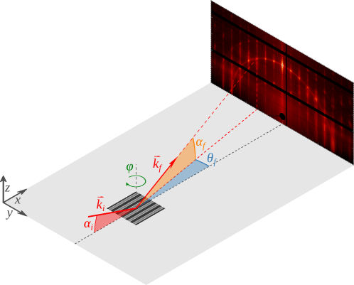
The measurement geometry of GISAXS Levine et al. [1989] is shown schematically in figure 1. The sample is illuminated under grazing incidence angle , and the resulting reflected and scattered radiation is collected with an area detector at exit angles and . We chose our coordinate system such that the --plane is the sample plane and the -axis lies in the scattering plane, with the -axis perpendicular to the sample plane. In this coordinate system, the scattering vector takes the form
| (1) | ||||
| (2) | ||||
| (3) |
with the wave vector of the incoming beam , the wave vector of the scattered beam , and the wavelength of the incident radiation.
2.3 Experimental Setup
The experiments were conducted at the four-crystal monochromator (FCM) beamline Krumrey and Ulm [2001] in the laboratory Beckhoff et al. [2009] of the Physikalisch-Technische Bundesanstalt (PTB) at the electron storage ring BESSY II. This beamline allows the adjustment of the photon energy in the range from to . The beam spot size was about at the sample position, with an estimated vertical coherence length projected onto the sample in the -direction of . The GISAXS setup at the FCM beamline consists of a sample chamber Fuchs et al. [1995] and the Helmholtz-Zentrum Berlin (HZB) SAXS setup Gleber et al. [2010]. The sample chamber is equipped with a goniometer which allows sample movements in all directions with a resolution of as well as rotations around all sample axes with an angular resolution of . The HZB SAXS setup allows the movement of the in-vacuum Pilatus 1M area detector Wernecke et al. [2014a], reaching sample-to-detector distances from about to about and exit angles up to approximately . Along the whole beam path including the sample site, a high vacuum (pressure below up to and including the sample site, pressure below between sample and detector) is maintained.
The measurements of the homogeneity of the EBL and NIL hexagonal samples were conducted at a photon energy of . All other measurements were conducted at a photon energy of . The distance from the sample to the detector was calibrated by triangulation using the position of the direct and specularly reflected beam on the detector at various detector positions (see supplementary material for details). The incident () and exit () angles were calibrated by first aligning the sample parallel to the incident X-ray beam () and then using the position of the specularly reflected beam on the detector at , which together with the distance from the sample to the detector yields the exact values for and . The orientation of the crystallographic direction to the x-ray beam was calibrated by tuning until the diffraction pattern was symmetric along the specular axis, yielding . For the homogeneity measurements, the angles were calibrated using the position of the attenuated direct beam taken without sample in the beam path and the specularly reflected beam on the detector, giving higher precision in the comparison of the different samples. The raw GISAXS data and used analysis scripts producing the graphics in this paper are available in the supplementary material.
2.4 Theoretical Description
We model the GISAXS measurements using the framework of the distorted wave Born approximation (DWBA) Vineyard [1982], Sinha et al. [1988], Renaud et al. [2009]. In the DWBA, the scattering cross section of a collection of particles is expressed as
| (4) |
with the position of the -th particle and its DWBA form factor Burle et al. [2016], Daillant and Gibaud [2009].
To describe the periodic samples, we use the decoupling approximation for the pillars Burle et al. [2016], assuming that all pillars have the same DWBA form factor . This allows us to separate the description of the form factor and the interference function
| (5) |
The interference function of a two-dimensional periodic lattice is
| (6) |
with the reciprocal lattice Burle et al. [2016].
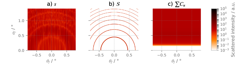
To describe the locally quasicrystalline samples, we separately describe the positions of the nanopillars in the supercell by explicitly enumerating each position within the supercell, and fill the plane by tiling supercells. In effect, we use the model of a two-dimensional crystal with a large unit cell. Figure 2 shows the different effects of the pillar positions within the supercell, the supercell tiling, and the form factor of the individual pillars. The calculations for figure 2 were done with a photon energy of , the corresponding refractive index of silicon oxide according to Henke et al. [1993] and an incident angle of .
The tiling of the supercells is described by an interference function again using the decoupling approximation between supercells Burle et al. [2016], stating that pillar properties in the same sample do not depend on the specific supercell the pillars are in. This leads to the expression
| (7) |
If we further assume that all pillars in a sample in each supercell have the same form and thus a uniform DWBA form factor , we can further simplify the expression as follows
| (8) | ||||
| (9) |
where contains only the effect of the positions of pillars in the locally quasicrystalline supercell and is given by the positions of the nanopillars known from the chosen design. An example of a result for is shown in figure 2a). A complex pattern of diffraction orders which are sharp in and elongated in can be seen. The distribution of the diffraction orders in the -direction arises from the local correlations in the -direction. In contrast, the distances between individual pillars cannot be resolved in the -direction, but the size of the rectangular supercell can be resolved and manifests itself in diffuse semicircles at constant that overlay the scattering pattern.
To be able to implement eq. (9) numerically, we have to find explicit expressions for and as well. For the tiling interference function , we use a one-dimensional lattice interference function in the -direction with a Gaussian decay function with decay length Burle et al. [2016], leading to
| (10) |
with the tiling period (see fig. 2b). In practice, due to the large angular distance between peaks in , it is sufficient to calculate the largest contribution with a single to the infinite sum, with . The tiling in the -direction can be neglected since the experimental resolution is not high enough to resolve the very dense spacing of peaks in . For the DWBA form factor , we use the general form Burle et al. [2016], Lazzari [2009]
| (11) | ||||||
| with | ||||||
| (12) | ||||||
| (13) | ||||||
| (14) | ||||||
| (15) | ||||||
where are the electric field amplitudes of the upwards (+) and downwards (-) travelling waves of the incoming (i) and final (f) waves as obtained from the dynamical calculation of the layer system without particles Gibaud and Vignaud [2009] and are the respective wave vectors. Since we are mainly interested in the locally quasicrystalline nature of the samples and not in the form of the pillars, we can set the Born form factor to a constant (see fig. 2c). Finally we get:
| (16) | ||||
| (17) |
3 Results
3.1 Comparison of periodic and locally quasiperiodic structures
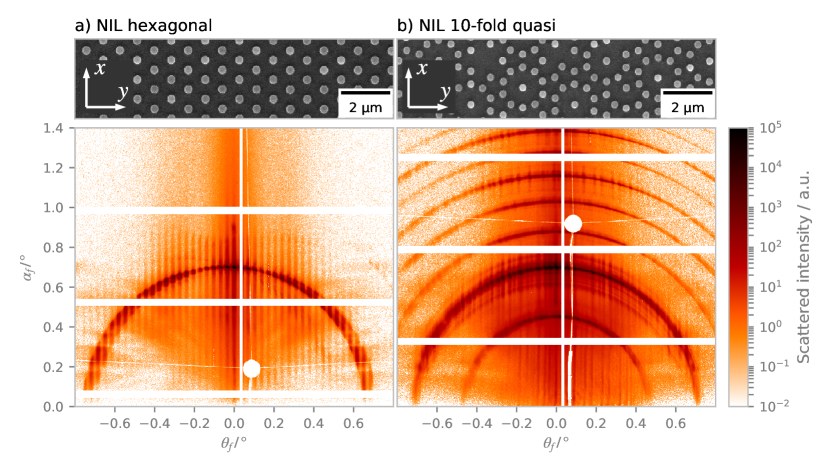
GISAXS measurements of the NIL hexagonal and NIL 10-fold quasi samples collected at an incident angle of and a sample-to-detector distance of are shown in figure 3. We aligned the crystallographic direction of the samples to the incident X-ray beam, as can be seen from the mirror symmetry of the diffraction patterns. The resolution of the measurements is limited by the divergence of the incident beam, and is .
The scattering pattern of the NIL hexagonal sample (fig. 3a) consists of diffraction orders forming a semicircle. The pattern can be described by the intersection of the reciprocal form of a hexagonal lattice with the Ewald sphere of elastic scattering (similarly to the reciprocal space construction of the scattering of line gratings as done by Mikulík et al. [2001] and Yan and Gibaud [2007]). The reciprocal form of a hexagonal lattice with lattice constant is a collection of lattice truncation rods that are parallel to the -axis and are arranged on a hexagonal lattice with lattice constant in the --plane. When the incident beam is aligned to a symmetry axis of the hexagonal lattice, the reciprocal form of the hexagonal lattice is aligned to the -axis, with lattice truncation rods at with the order . Intersecting the Ewald sphere with the lattice truncation rods yields diffraction peaks. The steep inclination of the Ewald sphere at small exit angles results in a small covered -range in GISAXS measurements. Therefore, only the diffraction peaks resulting from the zero-order lattice truncation rods at can be measured, leading to a semicircle of diffraction peaks, as seen in the scattering pattern. However, in contrast to the theory of a perfect hexagonal lattice, the diffraction orders are stretched in at higher , which we attribute to inhomogeneities within the sample pattern Rueda et al. [2012], Meier et al. [2012], Soccio et al. [2014] and discuss in detail in subsection 3.2.
The diffraction pattern of the NIL 10-fold quasi sample (fig. 3b) shows similarities and striking differences to the diffraction pattern of the NIL hexagonal sample. As in the diffraction of the periodic sample, there are diffraction orders forming a semicircle and the diffraction orders are stretched along due to inhomogeneities (in the example shown in figure 3b, the inhomogeneities are relatively small; a detailed description of the inhomogeneities is found in section 3.2). However, there are also two main differences. Firstly, additional, weaker semicircles appear above and below the semicircle at . They are caused by the long-range periodicity of the supercell design (compare section 2.4), with a period length of about in the -direction. Secondly, the diffraction orders show no periodicity within the semicircle, which is due to the short-range quasiperiodicity in the -direction. The long-range periodicity in the -direction cannot be resolved.
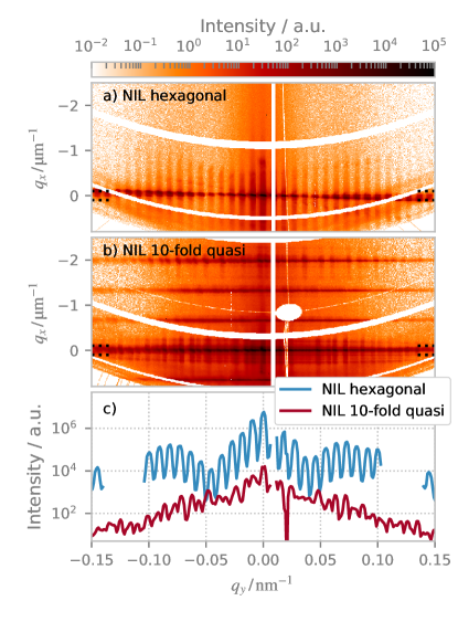
The periodicity in the -direction is more clearly visible after transforming the measurements according to eq. (1) into the --plane, shown in figure 4a) and figure 4b). The semicircles are transformed into straight lines spaced equally in . The intensity distribution along the -direction is readily visible in in-plane cuts taken by integrating along at , shown in figure 4c). While the measurement of the periodic sample shows equally spaced diffraction orders, the intensity of the locally quasiperiodic sample does not display a discernible periodicity.
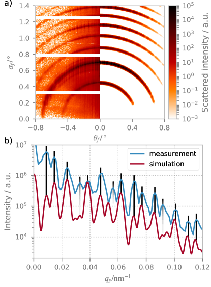
We simulated the diffraction of the NIL 10-fold quasi sample as detailed in subsection 2.4. For the tiling period, we use the design value of and set the decay length to . For the form factor , we use a constant and to calculate the DWBA prefactors , we assume a system consisting of three layers. At the top is a vacuum layer, at the bottom, the silicon oxide substrate and between them, an average density layer generated by the nanopillars. The average density layer also consists of silicon oxide with parameters according to the nanopillar design values. Its density is reduced to relative to bulk silicon oxide and the thickness of the layer is , the nominal height of the pillars. For the comparison of the simulated data with the measurement, a Debye-Waller factor with a mean roughness was introduced in the simulation. Additionally, to account for the beam divergence in the experiment, a Gaussian filter with a standard deviation of was applied to the simulation. A comparison of the measurement and simulation results for the NIL 10-fold quasi sample is shown in figure 5. The position and form of the semicircles match very well (fig. 5a). In the simulation, the position and form of the semicircles results from the tiling of the supercells which is described in section 2.4 by . To also assess the accuracy of our description of the locally quasicrystalline ordering within the supercells (described by ), we took a cut at , which is shown in figure 5b). The positions of the peaks agree well with only three peaks missing or shifted in the simulation, but the relative peak intensities match poorly. The comparison between the simulation and the measurement shows that our hierarchical model of tiled supercells with local quasicrystalline ordering can adequately describe the position of the coherent scattering features, but is not able to describe their relative intensity satisfactorily.
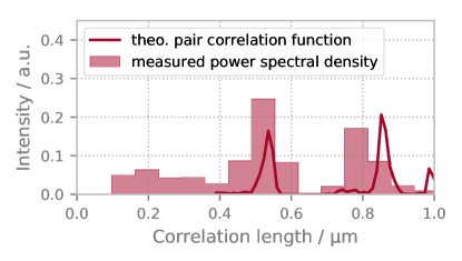
To obtain further insights in real space, we calculated the power spectral density of the in-plane cuts using the range of , which avoids all beam stop shadowing and detector gaps. The discrete Fourier transformation (DFT) was carried out using a Kaiser window Kaiser [1966]. For comparison with theoretical expectations, we computed the pair correlation function of the design pillar positions. The result for the NIL 10-fold quasi sample is shown in figure 6. The measured power spectral density shows two broad peaks at about and . Correspondingly, the theoretical pair correlation function of the design lattice shows two main peaks, at about and . The main peaks at about and agree quite well with the measurement and theoretical expectation and correspond to the nearest neighbour distance and the ring-like patterns in the sample, respectively (compare SEM image in figure 3b). However, a non-zero intensity between approximately and is not expected theoretically. We attribute this to the finite width of the pillars, which was not considered in the pair correlation function.
3.2 Lattice distortions
As noted, the diffraction patterns of the NIL samples show an elongation of the diffraction orders along at high . In this section, we use this elongation to quantify the inhomogeneity of all four samples, scanning along the -direction for the spatial resolution and characterization of the whole sample surface.
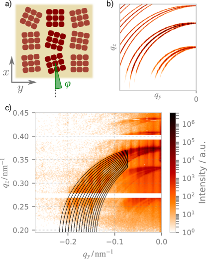
In section 2.4, we use the tiling interference function of a one-dimensional lattice in the -direction, which leads to scattering into a series of sharp arcs. To model the disturbed order in the locally quasiperiodic samples, we assume that the tiling is locally well ordered, but due to the manufacturing, several domains exist which have the tiling in a slightly different direction and therefore, different (see fig. 7a). Equivalently, we assume, for the periodic samples, that the structure is locally well ordered, but several domains exist which are oriented slightly differently. The domains are assumed to be large compared to the coherence length of the incident X-rays, and therefore the measured signal is the incoherent superposition of the signals of the domains illuminated by the X-ray beam (see fig. 7b). To describe the signal of a single domain rotated in the sample plane by the angle , we generalize . For the zero-order semicircle, this yields Mikulík et al. [2001], Yan and Gibaud [2007], Pflüger et al. [2017] in coordinate form:
| (18) | ||||
| (19) |
with the running auxiliary variable .
Using eqs. (18) and (19), the scattering image is cut into slices with differing and the intensity in each slice is integrated (see fig. 7c). For the slicing of the scattering image, a trade-off between signal intensity and resolution needs to be made. For high signal intensities, the slices need to be continued towards , because scattering at smaller is generally more intense due to roughness. On the other hand, the height of the slices decreases towards . Given a constant resolution in due to divergence or pixel size, extending the slices towards smaller will decrease the resolution. With the resolution in the exit angle of our setup of and our slicing range of , we have a resolution of about with acceptable signal-to-noise ratio.
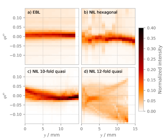
We took measurements of the three samples produced by nanoimprint lithography (NIL hexagonal, NIL 10-fold quasi and NIL 12-fold quasi) and of the EBL sample as a comparison. Since the elongated beam footprint is longer than the sample, each GISAXS measurement collects information on an approximately wide, full-length strip of the large sample. To gain insight into the spatial distribution of inhomogeneities, GISAXS measurements were taken in a scan along the -direction. The results are given in figure 8 and show the statistical inhomogeneities of each sample in an area of about .
The EBL reference sample shows a very narrow distribution, with no changes over . Apart from demonstrating the high quality of the E-beam lithography production process, the absence of any measurable drift also shows the angular stability of the measurement setup for sample movements. In contrast, the nanoimprinted samples all display larger inhomogeneities. Two (NIL hexagonal and NIL 10-fold quasi) show only slightly wider distributions, which however drift along . The NIL 12-fold quasi sample shows the largest inhomogeneities, both as wider distributions at each position and as a high shift along .
The results are condensed in figure 9, which presents the sum of all measurements along for each sample. It shows the very high quality of the E-beam lithography process, and the loss of homogeneity in the additional nanoimprinting processing steps. All three NIL samples were simultaneously manufactured on one substrate using one template, but they show differing homogeneity. The differences in homogeneity cannot be explained by the different lattice design, since each NIL sample shows large spatial variations in homogeneity in the scan in the -direction. We conclude that inhomogeneities were introduced in the nanoimprinting process, which can be explained with the flexible NIL template, which leads to small variations in the imprint. The absolute magnitude of the largest variations is still relatively small with . As explained in section 2.1, the nanoimprinting process was not optimized for the highest homogeneity.
4 Conclusion
To our knowledge, we report on the first GISAXS measurement of locally quasiperiodic surface structures, and compare them with simulations and with measurements of periodic samples. The measurements agree qualitatively with the theoretical description of the locally quasiperiodic samples as a hierarchically ordered system. The supercell gives rise to quasicrystalline diffraction at small length scales, and the tiling of the rectangular supercells leads to crystalline diffraction at longer length scales. Cuts of the GISAXS measurements in the -direction and their Fourier transform show the local quasiperiodicity and agree with the simulation and the calculated pair correlation function, respectively. Simultaneously, the long-range periodicity is revealed by GISAXS in the -direction due to the -resolution in . In contrast, the measurements of periodic samples show simple diffraction patterns arising from the short-range periodicity visible in .
With our theoretical description of rotated lattices, we are able to extract the distortions of the periodic supercell tiling of the locally quasicrystalline samples and the distortions of the periodic lattice of the periodic samples. We extract the lattice distortions on a area spatially resolved in the -direction. Because GISAXS is very sensitive to misalignments of the local lattice direction, we can resolve distortions down to . As expected, the EBL sample shows minimal lattice distortions over the whole sample, demonstrating the high quality achievable using electron beam lithography. Likewise, we find only small lattice misalignments in the nanoimprinted samples considering their intended use in the solar spectrum. However, in comparison to the EBL sample, the variations in homogeneity are considerably larger, with lattice misalignments up to . By optimizing the nanoimprinting process, the homogeneity of the nanoimprinted samples could likely be increased further.
We have shown that GISAXS is a suitable method to investigate complex surface designs intended for use in solar cells, and an extension to buried interfaces is desirable. However, to extract quantitative structure parameters of the investigated locally quasiperiodic samples from the GISAXS measurements, a more quantitative theoretical description would be needed. In particular, we neglected the Born form factor of the individual pillars, focussing on the positions of the pillars, but the average form of the pillars is also of interest for the intended application. However, for the reconstruction of the average form of the pillars, a more extensive dataset is likely necessary.
A comparison between locally quasiperiodic samples and globally quasiperiodic samples without long-range periodicity would be of special interest. For such a comparison, an interference function describing an infinite quasiperiodic lattice would need to be developed to describe the globally quasiperiodic samples in the distorted wave Born approximation. Unfortunately, due to manufacturing constraints, no such samples exist to our knowledge.
5 Acknowledgments
The authors wish to thank Levent Cibik and Stefanie Langner for their support during the experiments.
The German Ministry of Education and Research is acknowledged for funding the research activities of the Young Investigator Group Nano-SIPPE at HZB in the NanoMatFutur programme (no. 03X5520).
References
- Babonneau et al. [2009] D. Babonneau, S. Camelio, D. Lantiat, L. Simonot, and A. Michel. Waveguiding and correlated roughness effects in layered nanocomposite thin films studied by grazing-incidence small-angle x-ray scattering. Physical Review B, 80(15):155446, Oct. 2009. 10.1103/PhysRevB.80.155446.
- Becker et al. [2013] C. Becker, D. Amkreutz, T. Sontheimer, V. Preidel, D. Lockau, J. Haschke, L. Jogschies, C. Klimm, J. J. Merkel, P. Plocica, S. Steffens, and B. Rech. Polycrystalline silicon thin-film solar cells: Status and perspectives. Solar Energy Materials and Solar Cells, 119(Supplement C):112–123, Dec. 2013. ISSN 0927-0248. 10.1016/j.solmat.2013.05.043.
- Beckhoff et al. [2009] B. Beckhoff, A. Gottwald, R. Klein, M. Krumrey, R. Müller, M. Richter, F. Scholze, R. Thornagel, and G. Ulm. A quarter-century of metrology using synchrotron radiation by PTB in Berlin. physica status solidi (b), 246(7):1415–1434, July 2009. ISSN 1521-3951. 10.1002/pssb.200945162.
- Burle et al. [2016] J. Burle, C. Durniak, J. M. Fisher, M. Ganeva, G. Pospelov, W. Van Herck, and J. Wuttke. Born Again Manual, Dec. 2016.
- Daillant and Gibaud [2009] J. Daillant and A. Gibaud, editors. X-Ray and Neutron Reflectivity, volume 770 of Lecture Notes in Physics. Springer Berlin Heidelberg, Berlin, Heidelberg, 2009. ISBN 978-3-540-88587-0 978-3-540-88588-7.
- Eisenhauer et al. [2015] D. Eisenhauer, B. Pollakowski, J. Baumann, V. Preidel, D. Amkreutz, B. Rech, F. Back, E. Rudigier-Voigt, B. Beckhoff, B. Kanngieer, and C. Becker. Grazing incidence X-ray fluorescence analysis of buried interfaces in periodically structured crystalline silicon thin-film solar cells. physica status solidi (a), 212(3):529–534, Mar. 2015. ISSN 1862-6319. 10.1002/pssa.201400112.
- Fuchs et al. [1995] D. Fuchs, M. Krumrey, P. Müller, F. Scholze, and G. Ulm. High precision soft x-ray reflectometer. Review of Scientific Instruments, 66(2):2248–2250, Feb. 1995. ISSN 0034-6748, 1089-7623. 10.1063/1.1145720.
- Gann et al. [2014] E. Gann, A. Watson, J. R. Tumbleston, J. Cochran, H. Yan, C. Wang, J. Seok, M. Chabinyc, and H. Ade. Topographic measurement of buried thin-film interfaces using a grazing resonant soft x-ray scattering technique. Physical Review B, 90(24):245421, Dec. 2014. 10.1103/PhysRevB.90.245421.
- Gibaud and Vignaud [2009] A. Gibaud and G. Vignaud. Specular Reflectivity from Smooth and Rough Surfaces. X-ray and Neutron Reflectivity, 770:85–131, 2009. 10.1007/978-3-540-88588-7_3.
- Gleber et al. [2010] G. Gleber, L. Cibik, S. Haas, A. Hoell, P. Müller, and M. Krumrey. Traceable size determination of PMMA nanoparticles based on Small Angle X-ray Scattering (SAXS). Journal of Physics: Conference Series, 247:012027, Oct. 2010. ISSN 1742-6596. 10.1088/1742-6596/247/1/012027.
- Gu et al. [2012] Y. Gu, C. Wang, and T. P. Russell. Multi-Length-Scale Morphologies in PCPDTBT/PCBM Bulk-Heterojunction Solar Cells. Advanced Energy Materials, 2(6):683–690, June 2012. ISSN 1614-6840. 10.1002/aenm.201100726.
- Hagihara et al. [2017] K. Hagihara, R. Taniguchi, E. Yamanaka, K. Omote, Y. Ito, K. Ogata, and N. Hayashi. The capability of measuring cross-sectional profile for hole patterns in nanoimprint templates using small-angle x-ray scattering. In Photomask Technology, volume 10451, page 104510H. International Society for Optics and Photonics, Oct. 2017. 10.1117/12.2284761.
- Henke et al. [1993] B. L. Henke, E. M. Gullikson, and J. C. Davis. X-ray interactions: Photoabsorption, scattering, transmission, and reflection at E=50-30000 eV, Z=1-92. Atomic Data and Nuclear Data Tables, 254(2):181–342, July 1993. 10.1006/adnd.1993.1013.
- Hexemer and Müller-Buschbaum [2015] A. Hexemer and P. Müller-Buschbaum. Advanced grazing-incidence techniques for modern soft-matter materials analysis. IUCrJ, 2(1):106–125, Jan. 2015. ISSN 2052-2525. 10.1107/S2052252514024178.
- Holý et al. [1993] V. Holý, J. Kuběna, I. Ohlídal, K. Lischka, and W. Plotz. X-ray reflection from rough layered systems. Physical Review B, 47(23):15896–15903, June 1993. 10.1103/PhysRevB.47.15896.
- IUCr [2018] IUCr. Quasicrystal - Online Dictionary of Crystallography. http://reference.iucr.org/dictionary/Quasicrystal, June 2018.
- Jiang et al. [2011] Z. Jiang, D. R. Lee, S. Narayanan, J. Wang, and S. K. Sinha. Waveguide-enhanced grazing-incidence small-angle x-ray scattering of buried nanostructures in thin films. Physical Review B, 84(7):075440, Aug. 2011. 10.1103/PhysRevB.84.075440.
- Jones et al. [2003] R. L. Jones, T. Hu, E. K. Lin, W.-L. Wu, R. Kolb, D. M. Casa, P. J. Bolton, and G. G. Barclay. Small angle x-ray scattering for sub-100 nm pattern characterization. Applied Physics Letters, 83(19):4059–4061, Nov. 2003. ISSN 0003-6951. 10.1063/1.1622793.
- Kaiser [1966] J. F. Kaiser. Digital filters. In System Analysis by Digital Computer, pages 218–285. Wiley, New York, 1966.
- Krumrey and Ulm [2001] M. Krumrey and G. Ulm. High-accuracy detector calibration at the PTB four-crystal monochromator beamline. Nuclear Instruments and Methods in Physics Research Section A: Accelerators, Spectrometers, Detectors and Associated Equipment, 467:1175–1178, 2001. 10.1016/S0168-9002(01)00598-8.
- Lam et al. [2015] S. K. Lam, A. Pitrou, and S. Seibert. Numba: A LLVM-based Python JIT Compiler. In Proceedings of the Second Workshop on the LLVM Compiler Infrastructure in HPC, LLVM ’15, pages 7:1–7:6, New York, NY, USA, 2015. ACM. ISBN 978-1-4503-4005-2. 10.1145/2833157.2833162.
- Lazzari [2009] R. Lazzari. Grazing Incidence Small-Angle X-Ray Scattering from Nanostructures. X-ray and Neutron Reflectivity, 770:283–342, 2009. 10.1007/978-3-540-88588-7_7.
- Levine et al. [1989] J. R. Levine, J. B. Cohen, Y. W. Chung, and P. Georgopoulos. Grazing-incidence small-angle X-ray scattering: New tool for studying thin film growth. Journal of Applied Crystallography, 22(6):528–532, Dec. 1989. ISSN 00218898. 10.1107/S002188988900717X.
- Meier et al. [2012] R. Meier, H.-Y. Chiang, M. A. Ruderer, S. Guo, V. Körstgens, J. Perlich, and P. Müller-Buschbaum. In situ film characterization of thermally treated microstructured conducting polymer films. Journal of Polymer Science Part B: Polymer Physics, 50(9):631–641, May 2012. ISSN 1099-0488. 10.1002/polb.23048.
- Mikulík et al. [2001] P. Mikulík, M. Jergel, T. Baumbach, E. Majková, E. Pincik, S. Luby, L. Ortega, R. Tucoulou, P. Hudek, and I. Kostic. Coplanar and non-coplanar x-ray reflectivity characterization of lateral W/Si multilayer gratings. Journal of Physics D: Applied Physics, 34(10A):A188, 2001. 10.1088/0022-3727/34/10A/339.
- Millman and Aivazis [2011] K. J. Millman and M. Aivazis. Python for Scientists and Engineers. Computing in Science Engineering, 13(2):9–12, Mar. 2011. ISSN 1521-9615. 10.1109/MCSE.2011.36.
- Müller-Buschbaum [2014] P. Müller-Buschbaum. The Active Layer Morphology of Organic Solar Cells Probed with Grazing Incidence Scattering Techniques. Advanced Materials, 26(46):7692–7709, Dec. 2014. ISSN 09359648. 10.1002/adma.201304187.
- Müller-Buschbaum [2016] P. Müller-Buschbaum. GISAXS and GISANS as metrology technique for understanding the 3D morphology of block copolymer thin films. European Polymer Journal, Apr. 2016. ISSN 0014-3057. 10.1016/j.eurpolymj.2016.04.007.
- Pflüger et al. [2017] M. Pflüger, V. Soltwisch, J. Probst, F. Scholze, and M. Krumrey. Grazing-incidence small-angle X-ray scattering (GISAXS) on small periodic targets using large beams. IUCrJ, 4(4):431–438, July 2017. ISSN 2052-2525. 10.1107/S2052252517006297.
- Priolo et al. [2014] F. Priolo, M. Galli, T. F. Krauss, and T. Gregorkiewicz. Silicon nanostructures for photonics and photovoltaics. Nature Nanotechnology, 9(1):19, Jan. 2014. ISSN 1748-3395. 10.1038/nnano.2013.271.
- Renaud et al. [2009] G. Renaud, R. Lazzari, and F. Leroy. Probing surface and interface morphology with Grazing Incidence Small Angle X-Ray Scattering. Surface Science Reports, 64(8):255–380, Aug. 2009. ISSN 01675729. 10.1016/j.surfrep.2009.07.002.
- Rueda et al. [2012] D. R. Rueda, I. Martín-Fabiani, M. Soccio, N. Alayo, F. Pérez-Murano, E. Rebollar, M. C. García-Gutiérrez, M. Castillejo, and T. A. Ezquerra. Grazing-incidence small-angle X-ray scattering of soft and hard nanofabricated gratings. Journal of Applied Crystallography, 45(5):1038–1045, Oct. 2012. ISSN 0021-8898, 1600-5767. 10.1107/S0021889812030415.
- Shechtman et al. [1984] D. Shechtman, I. Blech, D. Gratias, and J. W. Cahn. Metallic Phase with Long-Range Orientational Order and No Translational Symmetry. Physical Review Letters, 53(20):1951–1953, Nov. 1984. 10.1103/PhysRevLett.53.1951.
- Sinha et al. [1988] S. K. Sinha, E. B. Sirota, S. Garoff, and H. B. Stanley. X-ray and neutron scattering from rough surfaces. Physical Review B, 38(4):2297–2311, Aug. 1988. 10.1103/PhysRevB.38.2297.
- Soccio et al. [2014] M. Soccio, N. Alayo, I. Martín-Fabiani, D. R. Rueda, M. C. García-Gutiérrez, E. Rebollar, D. E. Martínez-Tong, F. Pérez-Murano, and T. A. Ezquerra. On the assessment by grazing-incidence small-angle X-ray scattering of replica quality in polymer gratings fabricated by nanoimprint lithography. Journal of Applied Crystallography, 47(2):613–618, Apr. 2014. ISSN 1600-5767. 10.1107/S160057671400168X.
- Soltwisch et al. [2016] V. Soltwisch, A. Haase, J. Wernecke, J. Probst, M. Schoengen, S. Burger, M. Krumrey, and F. Scholze. Correlated diffuse x-ray scattering from periodically nanostructured surfaces. Physical Review B, 94(3):035419, July 2016. 10.1103/PhysRevB.94.035419.
- Soltwisch et al. [2017] V. Soltwisch, A. Fernández Herrero, M. Pflüger, A. Haase, J. Probst, C. Laubis, M. Krumrey, and F. Scholze. Reconstructing detailed line profiles of lamellar gratings from GISAXS patterns with a Maxwell solver. Journal of Applied Crystallography, 50(5):1524–1532, Oct. 2017. ISSN 1600-5767. 10.1107/S1600576717012742.
- Suck et al. [2002] J.-B. Suck, M. Schreiber, and P. Häussler. Quasicrystals: An Introduction to Structure, Physical Properties and Applications. Springer Verlag, Berlin Heidelberg New York, July 2002. ISBN 978-3-540-64224-4.
- Suh et al. [2016] H. S. Suh, X. Chen, P. A. Rincon-Delgadillo, Z. Jiang, J. Strzalka, J. Wang, W. Chen, R. Gronheid, J. J. de Pablo, N. Ferrier, M. Doxastakis, and P. F. Nealey. Characterization of the shape and line-edge roughness of polymer gratings with grazing incidence small-angle X-ray scattering and atomic force microscopy. Journal of Applied Crystallography, 49(3):823–834, June 2016. ISSN 1600-5767. 10.1107/S1600576716004453.
- Verschuuren and Sprang [2007] M. Verschuuren and H. V. Sprang. 3D Photonic Structures by Sol-Gel Imprint Lithography. MRS Online Proceedings Library Archive, 1002, Jan. 2007. ISSN 1946-4274, 0272-9172. 10.1557/PROC-1002-N03-05.
- Vineyard [1982] G. H. Vineyard. Grazing-incidence diffraction and the distorted-wave approximation for the study of surfaces. Physical Review B, 26(8):4146–4159, Oct. 1982. 10.1103/PhysRevB.26.4146.
- Wernecke et al. [2014a] J. Wernecke, C. Gollwitzer, P. Müller, and M. Krumrey. Characterization of an in-vacuum PILATUS 1M detector. Journal of Synchrotron Radiation, 21(3):529–536, May 2014a. ISSN 1600-5775. 10.1107/S160057751400294X.
- Wernecke et al. [2014b] J. Wernecke, H. Okuda, H. Ogawa, F. Siewert, and M. Krumrey. Depth-Dependent Structural Changes in PS-b-P2VP Thin Films Induced by Annealing. Macromolecules, 47(16):5719–5727, Aug. 2014b. ISSN 0024-9297, 1520-5835. 10.1021/ma500642d.
- Xavier et al. [2010] J. Xavier, M. Boguslawski, P. Rose, J. Joseph, and C. Denz. Reconfigurable Optically Induced Quasicrystallographic Three-Dimensional Complex Nonlinear Photonic Lattice Structures. Advanced Materials, 22(3):356–360, Jan. 2010. ISSN 1521-4095. 10.1002/adma.200901792.
- Xavier et al. [2014] J. Xavier, J. Probst, F. Back, P. Wyss, D. Eisenhauer, B. Löchel, E. Rudigier-Voigt, and C. Becker. Quasicrystalline-structured light harvesting nanophotonic silicon films on nanoimprinted glass for ultra-thin photovoltaics. Optical Materials Express, 4(11):2290–2299, Nov. 2014. ISSN 2159-3930. 10.1364/OME.4.002290.
- Xavier et al. [2016] J. Xavier, J. Probst, and C. Becker. Deterministic composite nanophotonic lattices in large area for broadband applications. Scientific Reports, 6, Dec. 2016. ISSN 2045-2322. 10.1038/srep38744.
- Yan and Gibaud [2007] M. Yan and A. Gibaud. On the intersection of grating truncation rods with the Ewald sphere studied by grazing-incidence small-angle X-ray scattering. Journal of Applied Crystallography, 40(6):1050–1055, Dec. 2007. ISSN 0021-8898. 10.1107/S0021889807044482.
- Zhou et al. [2012] J. Zhou, J. Wang, Y. Huang, G. Liu, L. Wang, S. Chen, X. Li, D. Wang, Y. Song, and L. Jiang. Large-area crack-free single-crystal photonic crystals via combined effects of polymerization-assisted assembly and flexible substrate. NPG Asia Materials, 4(8):e21, Aug. 2012. ISSN 1884-4057. 10.1038/am.2012.38.