Topological Boundary Modes from Translational Deformations
Abstract
Localized states universally appear when a periodic potential is perturbed by defects or terminated at its surface. In this Letter, we theoretically and experimentally demonstrate a mechanism that generates localized states through continuous translational deformations of periodic potentials. We provide a rigorous proof of the emergence of the localized states under the deformations. The mechanism is experimentally verified in microwave photonic crystals. We also demonstrate topological phase windings of reflected waves for translated photonic crystals.
In the 1930s, Tamm predicted the localized state of an electron near the surface of a solid Tamm (1932). Years later, Shockley proposed another mechanism that produces surface states, based on a band inversion of atomic orbitals Shockley (1939). Impurities and lattice defects inside a crystal also produce localized states James (1949); Saxon and Hunter (1949), which play important roles in doped semiconductors. While such localized states were first investigated for electrons, they universally appear in various wave systems. Zero-dimensional localized states have been observed in electronic superlattices Ohno et al. (1990), photonic and magnetophotonic crystals Yeh et al. (1978); Goto et al. (2008); Vinogradov et al. (2010), plasmonic crystals Kitahara et al. (2003, 2004); Guo et al. (2008); Sasin et al. (2008); Dyer et al. (2013), and phononic crystals Xiao et al. (2015).
The recent discovery of topological insulators has shed fresh light on the understanding of surface states in various wave systems from a topological perspective. Under time-reversal symmetry, bulk electronic states in band insulators are generally characterized by the topological invariant Kane and Mele (2005); Fu et al. (2007). The bulk-edge correspondence relates the bulk topological invariant to surface characteristics and ensures an existence of gapless boundary states with the Kramers degeneracy protected by time-reversal symmetry König et al. (2007); Chen et al. (2009). Later, it was shown that other discrete symmetries and their combinations generate various topological numbers for bulk electronic states and associated in-gap gapless boundary states Schnyder et al. (2008). A pioneering example is the topological invariant with a sublattice symmetry in the Su-Schrieffer-Heeger model Su et al. (1979, 1980). The nonzero topological integer in the Su-Schrieffer-Heeger model ensures zero-energy end states with sublattice-symmetry protection. For continuous one-dimensional crystals with inversion symmetry, Xiao et al. established a relation between surface observables and bulk properties and rigorously determined the existence or nonexistence of localized states Xiao et al. (2014). So far, research on one-dimensional systems has focused on unit cells with either sublattice or inversion symmetry to define the topological integers, but these discrete symmetries may not be essential, as suggested by Shockley Shockley (1939). In fact, the in-gap localized states as boundary states could survive under a gradual structural deformation that breaks the symmetries within the unit cell. This consideration indicates an alternative topological mechanism that generates localized states without using any symmetry protection.
In this letter, we devise a scheme that produces zero-dimensional localized states in a defect created by a translational deformation of a periodic potential. A rigorous proof of emergence of the localized states is provided without relying on any symmetry protection. The scheme is experimentally demonstrated in microwave photonic crystals.
Consider a one-particle eigenmode in one-dimensional continuous media with a periodic potential of the period . From the Bloch theorem Ashcroft and Mermin (1976), the eigenmode is characterized by the crystal momentum in the first Brillouin zone and the energy band index , where is periodic in . For simplicity, we assume that the eigenenergy of satisfies in the entire Brillouin zone. From here, we focus on the th band. The first Brillouin zone is discretized as with ( points). In terms of , a Wilson loop is given by
| (1) |
where and the inner product is defined in the unit cell Vanderbilt (2018). It is normalized to be unity as , where is simply the Zak phase Zak (1989). The Zak phase specifies a spatial displacement of the localized Wannier orbits that are composed only of the eigenmodes in the th energy band Vanderbilt (2018). In electronic systems, the Zak phase corresponds to surface charge, which can take a fractional value Vanderbilt and King-Smith (1993); Gangadharaiah et al. (2012); Park et al. (2016); Thakurathi et al. (2018).
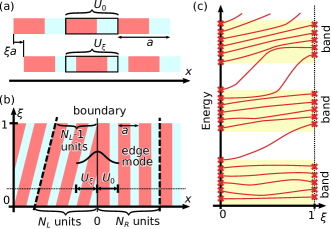
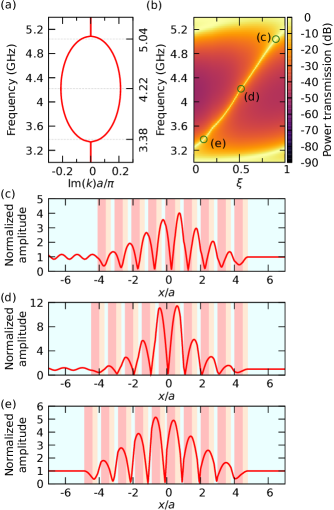
Now, let us translate continuously the one-dimensional periodic potential by () relative to a fixed frame of the unit cell. The spatial translation changes the potential configuration from to inside the fixed cell [see Fig. 1(a)]. When changes from 0 to 1, the localized Wannier orbit is continuously translated by the periodic length . Thus, it works like a classical screw pump Ozawa et al. (2019). Being identical to the displacement of the Wannier orbit with the unit-cell length (apart from a factor ), the Zak phase also continuously increases by under the translation: . The phase winding counts the Chern integer, which represents the topological characteristics of a fiber bundle on the plane Vanderbilt (2018); Asbóth et al. (2016). In this Letter, is regarded as a variable independent of other variables. Nonetheless, one could consider a continuous change of as a function of time . In particular, an adiabatic change of from 0 to 1 in suppresses interband transitions and is referred to as Thouless pumping Thouless (1983).
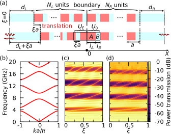
The phase winding in the Zak phase under the translation leads to a series of nontrivial localized states in a spatial boundary between two identical one-dimensional periodic systems with different translations . To see this, let us consider a periodic arrangement of unit cells with in a region of and another periodic arrangement of unit cells with in the other region of . The translation parameter and spatial coordinate subtend an extended two-dimensional space, as shown in Fig. 1(b). When changes from 0 to 1, the Zak phase in the former bulk region () winds up the phase. Meanwhile, the Zak phase in the latter bulk region () remains unchanged. Accordingly, the bulk-edge correspondence Thouless (1983); Asbóth et al. (2016); Vanderbilt (2018) suggests the existence of zero-dimensional edge states at the boundary region (), whose eigenenergies have “chiral” dispersions within a bulk band gap as a function of the translational parameter [Fig. 1(c)]. Moreover, as the Zak phase for any bulk band in the region of acquires the same phase winding during the translation, the number of the chiral dispersions between the th and th bulk bands are expected to be [Fig. 1(c)].
To prove this bulk-edge correspondence in the translational deformation rigorously, let us impose the following Born-von-Karman (BvK) boundary condition on a finite system [Fig. 1(b)]. Suppose that at , the entire one-dimensional system is comprised of unit cells in the region of and unit cells in the region of . For general , we identify with , such that the lattice periodicity is preserved at and it is broken only at . For and , the periodicity is completely preserved in the entire system, so that the eigenmodes at and are all spatially extended bulk band states. Under the BvK boundary condition, which discretizes the Brillouin zone, numbers of the bulk modes in each band at and at are given by and , respectively. Namely, the number of the extended bulk states decreases by one in each band when continuously changes from to . As the energy has a lower bound and there is no upper bound on the bulk band index in continuous media, more than one eigenmode in each bulk band at must move into bulk bands with a higher energy at during the translation of . For example, when one eigenmode in the lowest bulk band at goes to the second lowest bulk band at , two eigenmodes in the second lowest band at must go to the third lowest one at [Fig. 1(c)]. This argument inductively dictates that during the translation of , modes always raise their energies out of the th bulk energy band and go across the band gap between the th and th bands. An in-gap mode generally has a complex-valued wave number Cottey (1971). Accordingly, the in-gap modes must be spatially localized at , where the lattice periodicity is broken; therefore, they are simply defect modes localized at the boundary. Importantly, the argument so far does not require any symmetry protection for the presence of the in-gap localized states.
Now, we experimentally confirm the theoretical concept by using microstrip photonic crystals. A microstrip is a transmission line composed of a metallic strip separated from a conducting ground plane by a dielectric substrate. Microwaves propagate between the topside metallic strip and the backside ground plane, and the impedance and refractive index of a microstrip are determined by the geometrical parameters.
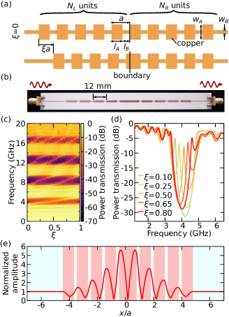
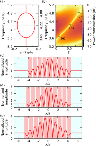
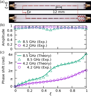
The first photonic system studied has a binary unit cell, in which the two strips with different widths behave as two different media. As shown schematically in Fig. 2(a), we continuously introduce a defect around the boundary by displacing the left half by while leaving the right half unchanged. A photograph of one of the fabricated samples () is provided in Fig. 2(b). Using a vector network analyzer (Keysight 5232A), we measured the power transmission through the samples with from to with a step size of . The transmission spectra obtained for these different are summarized in Fig. 2(c). Under , we clearly see five transmission bands, and four band gaps between them. The th band gap has boundary modes running between the two neighboring transmission bands, as expected from the theory. The qualitative behavior of the transmission spectra can be well captured by a transfer-matrix model calculation sup . Figure 2(d) shows some of the experimentally obtained power transmission spectra inside the first band gap. The transmission peak decreases and the line width becomes narrower around . This is because coupling between the incident wave and the boundary mode is reduced at the center of the band gap. In fact, the transfer-matrix model calculation confirms that the localized mode becomes the narrowest at the center of the first band gap sup , as plotted in Fig. 2(e).
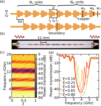
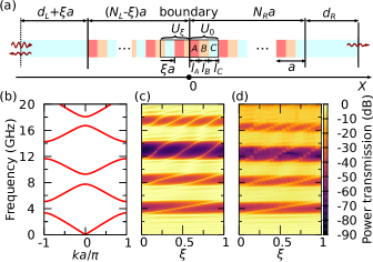
The second photonic system studied has three components in the unit cell. The design and photograph of the ternary microstrips are shown in Figs. 3(a) and 3(b), respectively. With three different regions, the unit cell has no spatial inversion symmetry at any . Figures 3(c) and 3(d) illustrate the experimental transmission spectra for 21 samples with different sup . These transmission spectra confirm that the localized modes run across the th transmission gap during the translation of from to . The experimental results clearly demonstrate that inversion symmetry is not essential for the generation of the series of localized states through translational deformation.
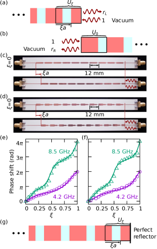
Next, we establish the physical origin of the localized states in terms of phase winding of the complex reflection amplitude. To this end, we divide the deformed crystal into two halves. Namely, the left region with is now terminated at its right end by a vacuum region, while the right region with is terminated by the same vacuum region at its left end [Figs. 4(a) and 4(b)]. Photonic properties of each semi-infinite region are characterized by the complex reflection amplitude or a relative surface impedance at the respective termination. The topological characteristics of localized states are encoded between the complex reflection amplitudes at both terminations and with an angular frequency . Specifically, a condition for eigenmodes localized at the original defect is nothing but the resonance condition across the two terminations: . The resonance condition can also be written as . When remains inside the band gap between the th and th bulk bands, both the semi-infinite regions behave as perfect reflectors: under assumption of no dissipation. Thus, the condition shows that the phase of must wind up by during the translation from to , because the boundary modes move across the angular frequency in the gap. The direction of the winding is determined by Foster’s theorem Collin (1996); sup .
The phase winding of the reflection is considered as the physical origin of the localized states. To confirm this phase winding experimentally, we fabricated samples composed only of the left-half parts with different , as in Figs. 4(c) and 4(d). Figures 4(e) and 4(f) show measured phases of the reflected waves of samples with different (relative to the measured phase at ). The experimental data points agree well with the theoretical curves obtained from the transfer-matrix model calculations for the semi-infinite systems sup . The results clearly demonstrate the presence of phase winding of the reflection amplitude, regardless of the unit-cell symmetry.
The phase winding of the reflection provides a unified perspective on both Tamm and Shockley states, which are often separately attributed to a perturbed surface potential and band inversion, respectively Tamm (1932); Shockley (1939); Vinogradov et al. (2010). To this end, we consider that the left region with is terminated by a perfect reflector at the right end as shown in Fig. 4(g). Given for those in the th transmission gap of the left part, the phase winding of during the translation of from 0 to 1 always guarantees the emergence of localized eigenmodes at the termination, irrespective of the details of the reflector on the right side. This holds true for any reflector with -independent perturbations, provided the perturbations maintain the perfect-reflection condition. Such perturbations include a delta-function-like surface perturbation, the existence of which distinguishes Tamm states from Shockley states, as discussed in Ref. Shockley (1939). In this sense, our proposed mechanism provides a comprehensive viewpoint for both Tamm and Shockley states.
In summary, we demonstrated a scenario that produces localized states through translational deformations analogous to classical screw pumping. The mechanism is not restricted to a specific physical system; rather, it is universal for any waves. Localized states in a system, even in the absence of sublattice or inversion symmetry, are now interpreted as topological boundary modes. The termination at the spatial boundary is understood as an engineered degree of freedom and can be used for tuning the spatial localization of the boundary mode.
The authors thank K. Usami, A. Noguchi, and M. W. Takeda for their fruitful discussions, and J. Koenig for his careful reading of the manuscript. This work was supported by JSPS KAKENHI (Grant No. 17K17777) and by the JST ERATO project (Grant No. JPMJER1601). R. S. was supported by National Basic Research Programs of China (973 program Grants No. 2014CB920901 and No. 2015CB921104) and National Natural Science Foundation of China (Grants No. 2017A040215).
References
- Tamm (1932) I. Tamm, Über eine mögliche art der elektronenbindung an kristalloberflächen, Phys. Z. Sowjetunion 1, 733 (1932).
- Shockley (1939) W. Shockley, On the surface states associated with a periodic potential, Phys. Rev. 56, 317 (1939).
- James (1949) H. M. James, Electronic states in perturbed periodic systems, Phys. Rev. 76, 1611 (1949).
- Saxon and Hunter (1949) D. S. Saxon and R. A. Hunter, Some electronic properties of a one-dimensional crystal model, Philips Res. Rep. 4, 81 (1949).
- Ohno et al. (1990) H. Ohno, E. E. Mendez, J. A. Brum, J. M. Hong, F. Agulló-Rueda, L. L. Chang, and L. Esaki, Observation of “Tamm states” in Superlattices, Phys. Rev. Lett. 64, 2555 (1990).
- Yeh et al. (1978) P. Yeh, A. Yariv, and A. Y. Cho, Optical surface waves in periodic layered media, Appl. Phys. Lett. 32, 104 (1978).
- Goto et al. (2008) T. Goto, A. V. Dorofeenko, A. M. Merzlikin, A. V. Baryshev, A. P. Vinogradov, M. Inoue, A. A. Lisyansky, and A. B. Granovsky, Optical Tamm States in One-Dimensional Magnetophotonic Structures, Phys. Rev. Lett. 101, 113902 (2008).
- Vinogradov et al. (2010) A. P. Vinogradov, A. V. Dorofeenko, A. M. Merzlikin, and A. A. Lisyansky, Surface states in photonic crystals, Phys. Usp. 53, 243 (2010).
- Kitahara et al. (2003) H. Kitahara, T. Kawaguchi, J. Miyashita, and M. Wada Takeda, Impurity mode in microstrip line photonic crystal in millimeter wave region, J. Phys. Soc. Jpn. 72, 951 (2003).
- Kitahara et al. (2004) H. Kitahara, T. Kawaguchi, J. Miyashita, R. Shimada, and M. Wada Takeda, Strongly localized singular Bloch modes created in dual-periodic microstrip lines, J. Phys. Soc. Jpn. 73, 296 (2004).
- Guo et al. (2008) J. Guo, Y. Sun, Y. Zhang, H. Li, H. Jiang, and H. Chen, Experimental investigation of interface states in photonic crystal heterostructures, Phys. Rev. E 78, 026607 (2008).
- Sasin et al. (2008) M. E. Sasin, R. P. Seisyan, M. A. Kalitteevski, S. Brand, R. A. Abram, J. M. Chamberlain, A. Y. Egorov, A. P. Vasil’ev, V. S. Mikhrin, and A. V. Kavokin, Tamm plasmon polaritons: Slow and spatially compact light, Appl. Phys. Lett. 92, 251112 (2008).
- Dyer et al. (2013) G. C. Dyer, G. R. Aizin, S. J. Allen, A. D. Grine, D. Bethke, J. L. Reno, and E. A. Shaner, Induced transparency by coupling of Tamm and defect states in tunable terahertz plasmonic crystals, Nat. Photonics 7, 925 (2013).
- Xiao et al. (2015) M. Xiao, G. Ma, Z. Yang, P. Sheng, Z. Q. Zhang, and C. T. Chan, Geometric phase and band inversion in periodic acoustic systems, Nat. Phys. 11, 240 (2015).
- Kane and Mele (2005) C. L. Kane and E. J. Mele, Topological Order and the Quantum Spin Hall Effect, Phys. Rev. Lett. 95, 146802 (2005).
- Fu et al. (2007) L. Fu, C. L. Kane, and E. J. Mele, Topological Insulators in Three Dimensions, Phys. Rev. Lett. 98, 106803 (2007).
- König et al. (2007) M. König, S. Wiedmann, C. Brüne, A. Roth, H. Buhmann, L. W. Molenkamp, X.-L. Qi, and S.-C. Zhang, Quantum spin Hall insulator state in HgTe quantum wells, Science 318, 766 (2007).
- Chen et al. (2009) Y. L. Chen, J. G. Analytis, J.-H. Chu, Z. K. Liu, S.-K. Mo, X. L. Qi, H. J. Zhang, D. H. Lu, X. Dai, Z. Fang, S. C. Zhang, I. R. Fisher, Z. Hussain, and Z.-X. Shen, Experimental realization of a three-dimensional topological insulator, Bi2Te3, Science 325, 178 (2009).
- Schnyder et al. (2008) A. P. Schnyder, S. Ryu, A. Furusaki, and A. W. W. Ludwig, Classification of topological insulators and superconductors in three spatial dimensions, Phys. Rev. B 78, 195125 (2008).
- Su et al. (1979) W. P. Su, J. R. Schrieffer, and A. J. Heeger, Solitons in Polyacetylene, Phys. Rev. Lett. 42, 1698 (1979).
- Su et al. (1980) W. P. Su, J. R. Schrieffer, and A. J. Heeger, Soliton excitations in polyacetylene, Phys. Rev. B 22, 2099 (1980).
- Xiao et al. (2014) M. Xiao, Z. Q. Zhang, and C. T. Chan, Surface Impedance and Bulk Band Geometric Phases in One-Dimensional Systems, Phys. Rev. X 4, 021017 (2014).
- Ashcroft and Mermin (1976) N. W. Ashcroft and N. D. Mermin, Solid State Physics (Holt, Rinehart and Winston, New York, 1976).
- Vanderbilt (2018) D. Vanderbilt, Berry Phases in Electronic Structure Theory: Electric Polarization, Orbital Magnetization and Topological Insulators (Cambridge University Press, Cambridge, England, 2018).
- Zak (1989) J. Zak, Berry’s Phase for Energy Bands in Solids, Phys. Rev. Lett. 62, 2747 (1989).
- Vanderbilt and King-Smith (1993) D. Vanderbilt and R. D. King-Smith, Electric polarization as a bulk quantity and its relation to surface charge, Phys. Rev. B 48, 4442 (1993).
- Gangadharaiah et al. (2012) S. Gangadharaiah, L. Trifunovic, and D. Loss, Localized End States in Density Modulated Quantum Wires and Rings, Phys. Rev. Lett. 108, 136803 (2012).
- Park et al. (2016) J.-H. Park, G. Yang, J. Klinovaja, P. Stano, and D. Loss, Fractional boundary charges in quantum dot arrays with density modulation, Phys. Rev. B 94, 075416 (2016).
- Thakurathi et al. (2018) M. Thakurathi, J. Klinovaja, and D. Loss, From fractional boundary charges to quantized Hall conductance, Phys. Rev. B 98, 245404 (2018).
- Ozawa et al. (2019) T. Ozawa, H. M. Price, A. Amo, N. Goldman, M. Hafezi, L. Lu, M. C. Rechtsman, D. Schuster, J. Simon, O. Zilberberg, and I. Carusotto, Topological photonics, Rev. Mod. Phys. 91, 015006 (2019).
- Asbóth et al. (2016) J. K. Asbóth, L. Oroszlány, and A. Pályi, A Short Course on Topological Insulators (Springer, Cham, Switzerland, 2016).
- Thouless (1983) D. J. Thouless, Quantization of particle transport, Phys. Rev. B 27, 6083 (1983).
- Cottey (1971) A. A. Cottey, Floquet’s theorem and band theory in one dimension, Am. J. Phys. 39, 1235 (1971).
- (34) See Supplemental Material for detailed information of the transfer-matrix method, comparison of theoretical and experimental transmission data, characterization of localized states, full reflection properties of the semi-infinite systems, and winding direction of complex reflection amplitudes.
- Collin (1996) R. E. Collin, Foundations for Microwave Engineering, 2nd ed. (McGraw-Hill, New York, 1996).
- Saleh and Teich (2007) B. E. A. Saleh and M. C. Teich, Fundamentals of Photonics, 2nd ed. (John Wiley & Sons, Inc., Hoboken, New Jersey, 2007).
- Hammerstad and Jensen (1980) E. Hammerstad and O. Jensen, Accurate models for microstrip computer-aided design, in 1980 IEEE MTT-S Int. Microwave Symp. Dig. (IEEE, Washington, 1980) pp. 407–409.
Supplemental Material for “Topological Boundary Modes from Translational Deformations”
.1 Transfer-matrix method
Here, we explain a calculation technique known as the transfer-matrix method for one-dimensional scalar wave propagation Saleh and Teich (2007); Collin (1996). Consider a two-port system with complex amplitudes , , , and of incoming and outgoing signals, as shown in Fig. S1. The scattering property of the system is modeled by a scattering matrix as
| (S1) |
To connect the systems, we also introduce a transfer matrix as
| (S2) |
By multiplying these transmission matrices, we obtain a total transmission matrix. The scattering and transfer matrices are related as follows: , , , and . Conversely, we have , , , and .

At a specific point in a one-dimensional photonic system, we can represent an electric field with an angular frequency as
| (S3) |
where we have an incoming complex amplitude , outgoing complex amplitude , vacuum impedance , and relative impedance with relative permittivity and relative permeability at the point in a material . Here, represents the complex conjugate of the preceding term. Note that we use the imaginary unit for a photonic system, and represents the coefficient of the imaginary part, which is represented by . At the boundary between two regions with material (left) and (right), we have the following scattering matrix:
| (S4) |
Correspondingly, we have as the transfer matrix for . For free propagation across a length in , we have the following transfer matrix:
| (S5) |
with wave number and speed of light in . By using a refractive index in , is written as , with the speed of light in a vacuum.
Now, we consider a unit cell of a photonic crystal with length of material from left to right (). The transfer matrix of the unit cell is defined as
| (S6) |
Eigenvalues of are given by with the complex Bloch wave number and the unit-cell length . From an eigenvector with (decaying to left) for inside a band gap, we can calculate by using with a vacuum for the model shown in Fig. 4(a) of the main text. The theoretical curves in Figs. 4(e) and 4(f) are calculated by this method, while we regard the wave-launching region as a “vacuum.”
To obtain the power transmission, we calculate a total transmission matrix for the entire system, and then convert it to the scattering matrix . Then, we have the power transmission for an incident wave from the left. Multiplying a series of transfer matrices to , we obtain the electric-field distribution.
.2 Comparison of theoretical and experimental transmission data
Here, we calculate transmission spectra of the binary and ternary photonic crystals [Figs. S3(a) and S3(a), respectively] and compare the results with the experimental data. The quasistatic refractive indices and impedances of the microstrips are calculated from formula derived by E. Hammerstad and O. Jensen Hammerstad and Jensen (1980). The calculated photonic bulk bands are shown in Figs. S3(b) and S3(b), and the expected transmission spectra are indicated in Figs. S3(c) and S3(c). We can see that the bulk bands in Figs. S3(b) and S3(b) correspond to the high transmission regions in Figs. S3(c) and S3(c), respectively. The experimental transmission spectra are also shown in Figs. S3(d) and S3(d). The experimental transmission power is not as high as that calculated in the higher frequency region. This is because losses (dielectric, metallic, or radiative) are not included in the model. The calculated transmission-band frequencies show good agreement with the experimental data, especially in the lower frequency region. Discrepancies in the higher frequency region can be attributed to the effect of dispersion in the microstrips, which is not taken into account in the model calculation. Nonetheless, the topological behaviors of the localized states that migrate across the transmission gaps agree very well between theory and experiment in the entire frequency region.
.3 Characterization of localized states
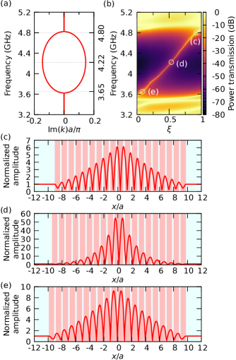
In this section, we characterize the field distribution of the localized states, based on the theoretical-model calculations. First, we analyze the binary photonic crystals. Generally, we have complex wave numbers inside band gaps. Figure S4(a) shows the imaginary part of the complex wave number inside the first band gap for the model. Near the center of the band gap, the imaginary part is maximized. Figure S4(b) shows the power transmission, which is enlarged from Fig. S3(c). To see the variation of the distribution, we took three points along the boundary-mode dispersion depicted as circles in Fig. S4(b). The corresponding field distributions are plotted in Figs. S4(c)–(e). As we expected from Fig. S4(a), localization is the narrowest in the center of the band gap. To observe the localization tuning more clearly, we increase from while the other parameters are left unchanged. The calculated results are summarized in Fig. S5. A comparison of Figs. S5(c)–(e) clearly shows the realization of the narrowest localization in the band-gap center. Thus, we can tune localization by altering , i.e., the termination. The narrowest localization decreases the coupling to the incident wave, and the radiative loss is reduced more effectively. For completeness, we also show data for the ternary photonic crystals in Fig. S6. The inversion-symmetry breaking leads to nonsymmetric field distributions in Figs. S6(c)–(e).
.4 Full reflection properties of the half systems
Here, we provide reflection-amplitude data for the half photonic crystals, in addition to the phase data of Figs. 4(e) and 4(f). Figures S7 and S8 show the complete data of reflection coefficients for the binary and ternary halves, respectively. The reflection amplitude should be unity in the theoretical models; however, it is degraded by the finite dissipation in the experiments. Slight changes in the reflection amplitudes with respect to are observed in Figs. S7(b) and S8(b). This can be attributed to the resonance, which is caused by a change in the length of the first strip located near the reflection boundary.
.5 Winding direction of complex reflection amplitudes
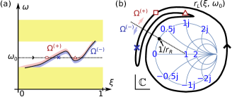
Based on Foster’s theorem, let us determine the rotation direction of from to for fixed inside a band gap. In this section, we focus on the band gap between the th and th bands. Thus, the total number of migrating localized modes from the th to th bands is .
The eigenfrequencies of localized modes inside the band gap are written as , which are determined by . Here, we consider the following regions with a small : and , where and . A possible situation for is graphically shown in Fig. S9. Foster’s reactance theorem can be applied, provided that the system is passive Collin (1996). Then, must monotonically rotate clockwise in the complex plane when we increase . Therefore, we have and for and , respectively.
Now, consider , with a specified inside the band gap. We assume there is no degeneracy of localized states at . In other words, we always have if . By changing from 0 to 1 along , the total number of transitions from to must be owing to the bulk-edge correspondence. In the Smith chart, corresponds to the situation that crosses over in an anti-clockwise manner. Similarly, represents clockwise crossing. Then, the winding number in the Smith chart must be in an anti-clockwise manner with changing from to because the trajectory is continuous. If there is an accidental degeneracy, we may consider an angular frequency that is slightly displaced from to avoid this degeneracy. Owing to the continuity, the winding number at must be the same as that at .