Thermoelectric conversion at in InAs/InP nanowire quantum dots
Abstract
We demonstrate high-temperature thermoelectric conversion in InAs/InP nanowire quantum dots by taking advantage of their strong electronic confinement. The electrical conductance and the thermopower are obtained from charge transport measurements and accurately reproduced with a theoretical model accounting for the multi-level structure of the quantum dot. Notably, our analysis does not rely on the estimate of co-tunnelling contributions since electronic thermal transport is dominated by multi-level heat transport. By taking into account two spin-degenerate energy levels we are able to evaluate the electronic thermal conductance and investigate the evolution of the electronic figure of merit as a function of the quantum dot configuration and demonstrate at , corresponding to an electronic efficiency at maximum power close to the Curzon-Ahlborn limit.
The progress in the fabrication and control of nanostructured systems has opened new prospects for thermoelectric (TE) research Hicks and Dresselhaus (1993); Mahan and Sofo (1996) and has provided new ways to create improved TE devices Dresselhaus et al. (2007); Vineis et al. (2010); Shi (2012); Sothmann et al. (2014); Benenti et al. (2017). In particular, quantum dots (QDs) were soon identified as ideal systems for the implementation of efficient heat engines Mahan and Sofo (1996) and for the creation of nanoscale thermometers Hoffmann et al. (2007). The key property is their discrete density of states that yields a strong energy selectivity in their transmission profile thus opening the way to the realization of TE systems with an optimized performance Mahan and Sofo (1996). As a consequence, TE effects in QDs have been extensively investigated both theoretically Beenakker and Staring (1992); Dzurak et al. (1998); Boese and Fazio (2001); Andreev and Matveev (2001); Turek and Matveev (2002); Koch et al. (2004); Kubala and König (2006); Zianni (2007); Kubala et al. (2008); Zianni (2008); Jacquet (2009); Costi and Zlatić (2010); Billings et al. (2010); Mani et al. (2011); Entin-Wohlman and Aharony (2012); Rejec et al. (2012); Jordan et al. (2013); López and Sánchez (2013); Kennes and Meden (2013); Dutt and Hur (2013); Muralidharan and Grifoni (2013); Sierra and Sánchez (2014); Svilans et al. (2016); Zimbovskaya (2015) and experimentally Dzurak et al. (1993); Staring et al. (1993); Molenkamp et al. (1994); Dzurak et al. (1997); Scheibner et al. (2007); Fahlvik Svensson et al. (2011); Svensson et al. (2013); Josefsson et al. (2018); Feshchenko et al. (2014); Dutta et al. (2017, 2018). The TE behavior of electronic devices is characterized by the so-called figure of merit that is larger in more efficient devices. Indeed, within linear-response regime, both the maximum efficiency and the efficiency at maximum power are solely determied by the figure of merit, and they are growing functions of ZT Benenti et al. (2017). The figure of merit is defined as , where is the electrical conductance, is the Seebeck coefficient, is the thermal conductance and is the temperature. In bulk materials the maximization of has been proved to be highly nontrivial since , and are intrinsically related. On the contrary, heat and charge transport in QD-based TE devices can be disentangled and larger values of can be achieved. The performance of thermal machines based on QDs has been theoretically studied by many authors Mani et al. (2011); Erdman et al. (2017); Zianni (2010); Sánchez and Büttiker (2011); Karlström et al. (2011); Trocha and Barnaś (2012); Jordan et al. (2013), while only one experimental investigation is available up to now Josefsson et al. (2018). We also note that QDs can provide a key building block for the fundamental investigation of quantum and stochastic thermodynamic effects, as shown for small-sized systems, where thermal fluctuations are of much relevance Blickle and Bechinger (2011); Pekola (2015); Roßnagel et al. (2016).
The investigation of TE effects in single-electron systems is performed in temperature regimes for which the thermal energy is smaller than the Coulomb gap. In addition, it is often desirable to implement devices where the individual energy levels are well-resolved with respect to the thermal energy so that only few levels contribute to the heat transport. Here, we exploit the strong confinement of QDs realized in InAs/InP heterostructured nanowires (NWs) Björk et al. (2004); Romeo et al. (2012); Rossella et al. (2014) to demonstrate field-effect control on the thermopower up to temperatures of the order of . The high temperature regime has been little explored in similar systems Svensson et al. (2013), usually operated at much lower temperatures Fahlvik Svensson et al. (2011); Josefsson et al. (2018). Our devices allow for the application of a temperature gradient along the NW, the measurement of charge current and the Seebeck coefficient, as well as the direct measurement of local temperatures. The strong confinement of the electrons in our QDs allows us to obtain charging energies exceeding , with inter-level spacings of the order of and thus to operate our devices at relatively high temperatures and close to the QD depletion. Using a theoretical model accounting for sequential tunnelling mediated by two spin-degenerate levels Beenakker (1991); Zianni (2008); Erdman et al. (2017) we can accurately reproduce the experimental conductance and thermopower. This allows us to estimate the electronic thermal conductance , the power factor and the electronic figure of merit .
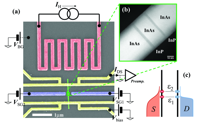
Fig. 1(a) shows a scanning electron micrograph of one of the investigated devices, where different colors correspond to different elements. The device core is constituted by an InAs/InP heterostructured NW with a diameter of . As visible in the Fig. 1(b), the nanostructure embeds a InAs island separated from the rest of the NW by two -wide InP barriers. The NWs used for this study were grown by Au-seeded chemical beam epitaxy Zannier et al. (2018) and have a wurtzite crystal structure. As grown NWs were detached from the growth substrate by sonication in isopropyl alcohol (IPA) and randomly deposited on a SiO2/Si p++ substrate by drop-casting and contacted by e-beam lithography followed by an evaporation of a metallic Ti/Au () bilayer. The resulting device layout includes a metallic serpentine heater (red), which can be fed by a current to induce, thanks to Joule heating, a thermal gradient along the NW (green). Our architecture also includes a set of multiple contact electrodes (yellow) that allows to: (i) apply a voltage bias and measure the current flowing through the NW; (ii) perform a local measurement of the temperature by tracking the resistance of the central metallic part of the contact electrodes. The QD population and spectrum can be controlled by a set of field-effect gates including the SiO2/Si p++ substrate, or back-gate (gray), and two side gates that can also be used to modify the radial confinement profile of the QD (purple) Roddaro et al. (2011).
The control on the temperature of the system is obtained by setting the temperature of the bath in which the device is immersed and then by setting a temperature gradient across the NW so that its hot end is at a temperature and its cold end is at a temperature . The average temperature is set high enough () so that we can benefit of the following advantages. (i) Since (where is the characteristic tunnelling rate through the QD barriers) and is not much larger than , sequential tunnelling processes dominate the thermoelectric transport and data analysis is relatively straightforward (see below for details); (ii) Since , non-linear response effects in thermal bias are negligible thus simplifying the theoretical analysis; (iii) charge transport can be explored for relatively large applied bias voltages (up to ) while remaining in the linear response regime. In this situation, the current flowing through the QD is given by
| (1) |
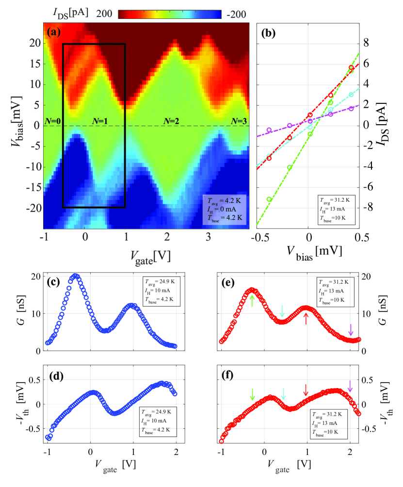
where is the electrical conductance and is the Seebeck coefficient. The thermovoltage at open circuit conditions is thus given by . It should be noted that both and are temperature dependent even if not explicitly indicated. Typical transport data from our QDs can be seen in Fig. 2(a), reporting a colorplot of as a function of the gate voltage and the DS bias at . Any of the three available gates (SG1, SG2 and BG) can be used to operate the device, but in the experiment reported here the QD was controlled using the lateral gate SG1 because it yielded the most stable control of the electronic configuration. Coulomb diamonds are clearly visible for various QD filling numbers , and indicate a charging energy on the first spin-degenerate level and an inter-level spacing . In Fig. 2(a) corresponds to a completely depleted QD, as further discussed in the Supplementary Information and as indicated by high-temperature transport data. However, the behavior of the device is not expected to critically depend on the presence of filled levels as long as they are far away in energy with respect to the relevant energy scales, in particular . In Fig. 2(b) we report a set of curves corresponding to vertical cross-sections at fixed taken from the region highlighted by the black rectangle in panel (a). The thermoelectric response of the device has been obtained from transport data in the linear regime. From the curve curve restricted to the linear response range (see e.g. Fig 2 (b)), we determine (slope) and (intercept) for each value and for a fixed using Eq. (1). From the knowledge of the slope and intercept of the lines it is possible to compute . Fig. 2(c)-(f) show the plots of and for two different bath temperatures and heating currents , such that the average temperatures of the QD are in panels (c) and (e) and in panels (d) and (f), respectively.
Experimental data are analyzed with a theoretical model based on a master equation accounting for sequential tunneling of electrons between the leads and the QD Beenakker and Staring (1992); Nazarov and Banter (2009); Erdman et al. (2017). As already mentioned in the introduction, we can reasonably assume that co-tunneling processes are negligible when two conditions are met, namely and . The first condition is required since small values of suppress the coefficient of co-tunneling rates. The second condition comes from the fact that co-tunneling contributions decay as a power law with the energy difference between the chemical potential of the leads and the nearest resonance (measured in units of ) Nazarov and Banter (2009). This means that they may prevail over sequential contributions for large enough , since sequential tunneling contributions decay exponentially with Beenakker (1991); Averin and Nazarov (1992); Nazarov and Banter (2009). Remarkably, the presence of two spin-degenerate levels, with spacing equal to , sets a bound to the energy difference . The second condition (for which ), therefore, ensures that the exponential suppression of sequential tunneling is limited and we can safely disregard co-tunneling effects. This is particularly relevant for values of such that the chemical potential of the leads is between the two spin-degenerate levels, where the thermopower is maximal even though the conductance is negligible.
Two spin-degenerate QD orbitals and are taken into account in the QD model and tunneling rates are assumed to depend on the number of electrons in the QD (see Supplementary Information for details about the model). Further important outputs of the fitting procedure are the electronic temperatures and that can be used to obtain a better estimate of the net temperature bias across the QD structure . The average fit temperature matches nicely with the one obtained experimentally sing the metallic thermometers , and confirms the good calibration of the resistive thermometers. On the contrary, is sizably smaller than . This is not very surprising since the NW has a finite heat conductance leading to a partitioning of the thermal bias as observed in experiments at lower temperatures Hoffmann et al. (2009). Since is the relevant temperature bias for the analysis of the TE response of the QD, it has been used for all the subsequent estimates on the TE parameters of the nanostructure.
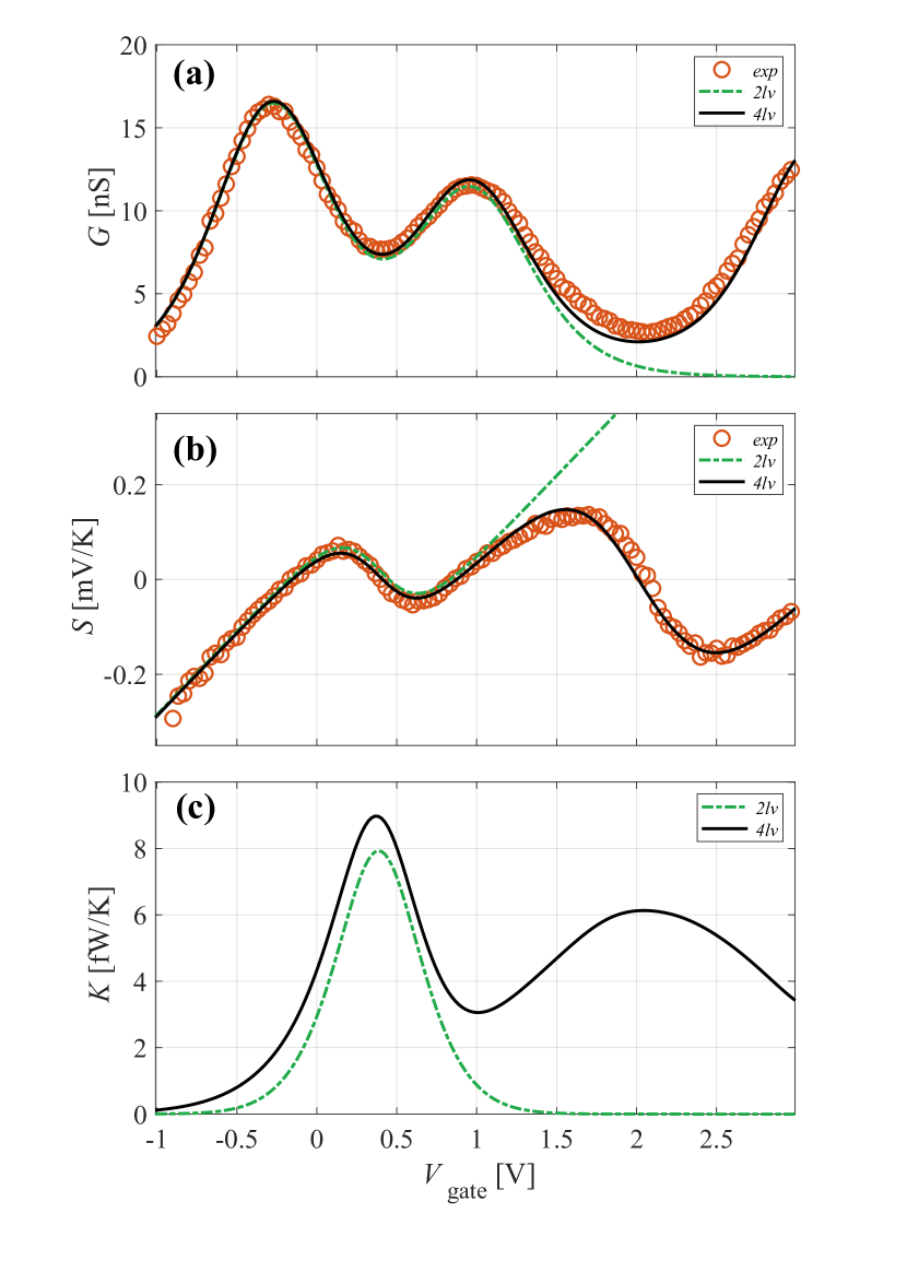
Fig. 3(a) and (b) show the experimental data (red dots) for the case , together with the fitted curves (solid lines) obtained using the model ( K). Different fitting models are compared: the solid black curve accounts for two spin-degenerate energy levels in the QD (here referred to as the “four-level” model); the green dashed curve accounts for a single (spin-degenerate) energy level (referred as the “two-level” model), as often done in the literature to model single Murphy et al. (2008); Esposito et al. (2009); Entin-Wohlman et al. (2010); Nakpathomkun et al. (2010); Mazza et al. (2014) and double quantum dot system Sánchez and Büttiker (2011); Trocha and Barnaś (2012); Jordan et al. (2013); Bhandari et al. (2018); Erdman et al. (2018). We notice that the four-level model nicely fits the experimental data for and in the whole range of values of under consideration, while the two-level model is accurate only for values in the conductance plot (the first two peaks in Fig. 3(a)) and up to in the thermopower plot (Fig. 3(b)). The theory can now be employed to calculate the electronic thermal conductance by using the fitting parameters obtained from the experimental data and (see Supplementary Information for details about values obtained for the parameters). The resulting curves for the two models are plotted in Fig. 3(c). Remarkably, the curve relative to the two-level model departs even in the first peak from the curve of the four-level model. This is due to the fact that K, by definition, is the ratio between the heat current and the temperature difference in open circuit conditions, i.e. when is zero. In a sequential single-level model, all electrons tunnel through the QD at the same energy, thus the same amount of heat is transferred to/from a given reservoirs in each tunneling event. If , there is not net transfer of charge, thus there is no net transfer of heat. This implies K=0, regardless of the gate voltage. Conversely, if there are two or more energy levels, electrons can tunnel at different energies, and this possibility allows for a net heat transfer at zero charge current Zianni (2008); Erdman et al. (2017). Therefore, as opposed to G and S, the value of K in the sequential regime is fully determined by the multilevel structure of the QD. It is thus crucial to employ the four-level model to estimate it properly.
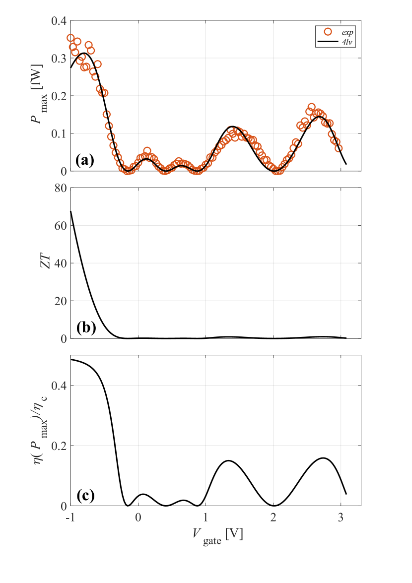
Using the three transport coefficients , and one can evaluate the performance of our QD system when operated as a heat engine. Indeed, the electric response to a temperature difference can be used to drive a current against a voltage bias, effectively extracting work from the system. The efficiency of a heat engine is then defined as the ratio between the extracted work and the heat provided by the hot reservoir. At fixed and temperature difference, we define as the maximum power that can be extracted by optimizing over the applied . The corresponding efficiency will then be the efficiency at maximum power ). It can be shownBenenti et al. (2017)) that also corresponds to the maximum power that can be performed on a variable load resistance in series with the QD. However, as shown in Ref.Benenti et al. (2017), within the linear response regime both and can be computed simply from the knowledge of the transport coefficients G, S and K previously shown, i.e. and , where is the electronic figure of merit. The maximum power is plotted in Fig. 4(a) as a function of the gate voltage using the theoretical (solid curve) and experimental (red circles) values of and together with the fitted value of . The experimental data (available down to ) is well reproduced by the four-level model which presents several peaks, the largest one corresponding to occurring at . Remarkably, the corresponding value of the electronic figure of merit [plotted in Fig. 4(b)] is . displays a fast increase as decreases below the first conductance peak, as expected for a single-level QD. This is due to the fact that there are no levels below the first conductance peak, so that our QD system approximately satisfies the requirement for achieving Carnot efficiency Mahan and Sofo (1996). Indeed, the electronic efficiency at maximum power, plotted in Fig. 4(c), takes the value (where is Carnot’s efficency) for , implying that our QD system can be operated at an electronic efficiency at maximum power very close to the Curzon-Ahlborn’s linear response upper bound . It is worth observing that the electronic efficiency at maximum power is computed from the knowledge of ZT Benenti et al. (2017). Interestingly, Fig. 4(c) shows that the electronic efficiency at maximum power roughly behaves as the maximum power [Fig. 4(a)], implying that both the maximum power and corresponding efficiency can be simultaneously maximized.
In conclusion, we have explored TE phenomena in InAs/InP NW QD-based devices at high temperature in the linear regime. Experimental data were analyzed using a multi-level model based on the resolution of a master equation which allowed us to compute the electronic thermal conductance of the system. This, in combination with the experimental data of conductance and thermopower, allowed us to estimate the electronic thermoelectric figure of merit and the electronic efficiency at maximum power of our thermoelectric engine. We find that the ideal Curzon-Ahlborn’s upper bound is nearly attained, and that a figure of merit is reached while extracting the maximum power from the system. This study demonstrates the full electrostatic control of the heat engine features of a thermally biased NW QD operating in high temperature regimes. Our results shed light on the operation of few level thermoelectric engines, a key issue for the physics and technology addressing heat and charge transport mediated by single carrier. The electronic ZT, which neglects the contribution of the phonons to the thermal conductance, is a sound characterization of the electronic properties of the device which allows to compare the electronic performance of different thermoelectric materials. Furthermore, it is directly related to the efficiency of non-equilibrum devices, such as solars cells which aim at recovering the energy of out-of-equilibrium ”hot carriers” excited by light Limpert et al. (2015, 2017). Possible applications include on-chip cooling, energy harvesting on cryogenic platforms and nanoscale thermometry.
We thank R. Fazio for helpul discussions and H. Courtois for carefully reading the manuscript. This work has also been supported by the SNS-WIS joint lab QUANTRA, by the SUPERTOP project, QUANTERA ERA-NET Cofound in Quantum Technologies and by the CNR-CONICET cooperation programme Energy conversion in quantum, nanoscale, hybrid devices.
Materials and Methods. InAs/InP heterostructured NWs were fabricated using a chemical beam epitaxy process seeded by metallic nanoparticles obtained from thermal dewetting of a Au thin film Gomes et al. (2015). Growth was performed at 420 10 C using trimethylindium (TMIn), tert-butylarsine (TBA), and tributylphosphine (TBP). The TBAs and TBP are thermally cracked at around 1000 C upon entering the growth chamber, while the TMIn decomposes on the substrate surface. The metallorganic pressures were 0.3, 1.0, and 4.0 Torr for TMIn, TBAs, and TBP, respectively. These growth conditions ensure to achieve InAs/InP NW heterostructures with straight morphology, constant diameter, wurtzite crystal structure and atomically sharp interfaces Zannier et al. (2017, 2018). InAs/InP and InP/InAs interfaces where realized without any interruption by switching the group V precursors. The position of the dot inside the NW is determined based on its average distance from the Au nanoparticle, as measured from an ensemble of wires with STEM. This leads to a typical alignment error of 50 nm, based on NW imaging statistics and on alignment errors during the lithographic process. Ohmic contacts are obtained by thermal evaporation of a Ti/Au (10/100 nm) bilayer, after a chemical passivation step based on a standard solution. The NW voltage bias was obtained using the auxiliary output of a Stanford Research lock-in amplifier SR830 and a resistor divider. Charge current was measured using a DL1211 current preamplifier and an Agilent 34401A multimeter. Each of the thermometers was excited by an AC current of , obtained using the sinusoidal output of a SR830 amplifier connected to a bias resistor. The local heater was supplied using a Keithley 2400 SourceMeter. The gate voltage was controlled using a Yokogawa 7651 DC source.
I Supplementary Information
-
•
Experimental methods: measurement setup, thermometers and heaters calibration, device characterization;
-
•
Details about the theoretical models involved in this study;
References
- Hicks and Dresselhaus (1993) L. D. Hicks and M. S. Dresselhaus, Phys. Rev. B 47, 12727 (1993).
- Mahan and Sofo (1996) G. D. Mahan and J. O. Sofo, Proceedings of the National Academy of Sciences 93, 7436 (1996), http://www.pnas.org/content/93/15/7436.full.pdf .
- Dresselhaus et al. (2007) M. Dresselhaus, G. Chen, M. Tang, R. Yang, H. Lee, D. Wang, Z. Ren, J.-P. Fleurial, and P. Gogna, Advanced Materials 19, 1043 (2007).
- Vineis et al. (2010) C. J. Vineis, A. Shakouri, A. Majumdar, and M. G. Kanatzidis, Advanced Materials 22, 3970 (2010).
- Shi (2012) L. Shi, Nanoscale and Microscale Thermophysical Engineering 16, 79 (2012).
- Sothmann et al. (2014) B. Sothmann, R. Sánchez, and A. N. Jordan, Nanotechnology 26, 032001 (2014).
- Benenti et al. (2017) G. Benenti, G. Casati, K. Saito, and R. S. Whitney, Physics Reports 694, 1 (2017).
- Hoffmann et al. (2007) E. A. Hoffmann, N. Nakpathomkun, A. I. Persson, H. Linke, H. A. Nilsson, and L. Samuelson, Applied Physics Letters 91, 252114 (2007).
- Beenakker and Staring (1992) C. W. J. Beenakker and A. A. M. Staring, Phys. Rev. B 46, 9667 (1992).
- Dzurak et al. (1998) A. Dzurak, C. Smith, C. Barnes, M. Pepper, L. Martín-Moreno, C. Liang, D. Ritchie, and G. Jones, Physica B: Condensed Matter 249-251, 281 (1998).
- Boese and Fazio (2001) D. Boese and R. Fazio, Europhysics Letters (EPL) 56, 576 (2001).
- Andreev and Matveev (2001) A. V. Andreev and K. A. Matveev, Physical Review Letters 86, 280 (2001).
- Turek and Matveev (2002) M. Turek and K. A. Matveev, Physical Review B 65 (2002), 10.1103/physrevb.65.115332.
- Koch et al. (2004) J. Koch, F. von Oppen, Y. Oreg, and E. Sela, Physical Review B 70 (2004), 10.1103/physrevb.70.195107.
- Kubala and König (2006) B. Kubala and J. König, Physical Review B 73 (2006), 10.1103/physrevb.73.195316.
- Zianni (2007) X. Zianni, Physical Review B 75 (2007), 10.1103/physrevb.75.045344.
- Kubala et al. (2008) B. Kubala, J. König, and J. Pekola, Physical Review Letters 100 (2008), 10.1103/physrevlett.100.066801.
- Zianni (2008) X. Zianni, Physical Review B 78 (2008), 10.1103/physrevb.78.165327.
- Jacquet (2009) P. A. Jacquet, Journal of Statistical Physics 134, 709 (2009).
- Costi and Zlatić (2010) T. A. Costi and V. Zlatić, Physical Review B 81 (2010), 10.1103/physrevb.81.235127.
- Billings et al. (2010) G. Billings, A. D. Stone, and Y. Alhassid, Physical Review B 81 (2010), 10.1103/physrevb.81.205303.
- Mani et al. (2011) P. Mani, N. Nakpathomkun, E. A. Hoffmann, and H. Linke, Nano Letters 11, 4679 (2011), pMID: 22003818, http://dx.doi.org/10.1021/nl202258f .
- Entin-Wohlman and Aharony (2012) O. Entin-Wohlman and A. Aharony, Physical Review B 85 (2012), 10.1103/physrevb.85.085401.
- Rejec et al. (2012) T. Rejec, R. Žitko, J. Mravlje, and A. Ramšak, Physical Review B 85 (2012), 10.1103/physrevb.85.085117.
- Jordan et al. (2013) A. N. Jordan, B. Sothmann, R. Sánchez, and M. Büttiker, Phys. Rev. B 87, 075312 (2013).
- López and Sánchez (2013) R. López and D. Sánchez, Physical Review B 88 (2013), 10.1103/physrevb.88.045129.
- Kennes and Meden (2013) D. M. Kennes and V. Meden, Physical Review B 87 (2013), 10.1103/physrevb.87.075130.
- Dutt and Hur (2013) P. Dutt and K. L. Hur, Physical Review B 88 (2013), 10.1103/physrevb.88.235133.
- Muralidharan and Grifoni (2013) B. Muralidharan and M. Grifoni, Physical Review B 88 (2013), 10.1103/physrevb.88.045402.
- Sierra and Sánchez (2014) M. A. Sierra and D. Sánchez, Physical Review B 90 (2014), 10.1103/physrevb.90.115313.
- Svilans et al. (2016) A. Svilans, A. M. Burke, S. F. Svensson, M. Leijnse, and H. Linke, Physica E: Low-dimensional Systems and Nanostructures 82, 34 (2016).
- Zimbovskaya (2015) N. A. Zimbovskaya, The Journal of Chemical Physics 142, 244310 (2015).
- Dzurak et al. (1993) A. Dzurak, C. Smith, M. Pepper, D. Ritchie, J. Frost, G. Jones, and D. Hasko, Solid State Communications 87, 1145 (1993).
- Staring et al. (1993) A. A. M. Staring, L. W. Molenkamp, B. W. Alphenaar, H. van Houten, O. J. A. Buyk, M. A. A. Mabesoone, C. W. J. Beenakker, and C. T. Foxon, EPL (Europhysics Letters) 22, 57 (1993).
- Molenkamp et al. (1994) L. Molenkamp, A. A. M. Staring, B. W. Alphenaar, H. van Houten, and C. W. J. Beenakker, Semiconductor Science and Technology 9, 903 (1994).
- Dzurak et al. (1997) A. S. Dzurak, C. G. Smith, C. H. W. Barnes, M. Pepper, L. Martín-Moreno, C. T. Liang, D. A. Ritchie, and G. A. C. Jones, Physical Review B 55, R10197 (1997).
- Scheibner et al. (2007) R. Scheibner, E. G. Novik, T. Borzenko, M. König, D. Reuter, A. D. Wieck, H. Buhmann, and L. W. Molenkamp, Physical Review B 75 (2007), 10.1103/physrevb.75.041301.
- Fahlvik Svensson et al. (2011) S. Fahlvik Svensson, A. I. Persson, E. A. Hoffmann, N. Nakpathomkun, H. Nilsson, H. Q Xu, L. Samuelson, and H. Linke, New. J. Phys., 14 (2011).
- Svensson et al. (2013) S. F. Svensson, E. A. Hoffmann, N. Nakpathomkun, P. M. Wu, H. Q. Xu, H. A. Nilsson, D. Sánchez, V. Kashcheyevs, and H. Linke, New Journal of Physics 15, 105011 (2013).
- Josefsson et al. (2018) M. Josefsson, A. Svilans, A. M. Burke, E. A. Hoffmann, S. Fahlvik, C. Thelander, M. Leijnse, and H. Linke, Nature Nanotechnology 13, 920 (2018).
- Feshchenko et al. (2014) A. V. Feshchenko, J. V. Koski, and J. P. Pekola, Phys. Rev. B 90, 201407 (2014).
- Dutta et al. (2017) B. Dutta, J. T. Peltonen, D. S. Antonenko, M. Meschke, M. A. Skvortsov, B. Kubala, J. König, C. B. Winkelmann, H. Courtois, and J. P. Pekola, Phys. Rev. Lett. 119, 077701 (2017).
- Dutta et al. (2018) B. Dutta, D. Majidi, A. G. Corral, P. Erdman, S. Florens, T. Costi, and H. C. C. B. Winkelmann, https://arxiv.org/abs/1811.04219 (2018).
- Erdman et al. (2017) P. A. Erdman, F. Mazza, R. Bosisio, G. Benenti, R. Fazio, and F. Taddei, Phys. Rev. B 95, 245432 (2017).
- Zianni (2010) X. Zianni, Physical Review B 82 (2010), 10.1103/physrevb.82.165302.
- Sánchez and Büttiker (2011) R. Sánchez and M. Büttiker, Phys. Rev. B 83, 085428 (2011).
- Karlström et al. (2011) O. Karlström, H. Linke, G. Karlström, and A. Wacker, Physical Review B 84 (2011), 10.1103/physrevb.84.113415.
- Trocha and Barnaś (2012) P. Trocha and J. Barnaś, Physical Review B 85 (2012), 10.1103/physrevb.85.085408.
- Blickle and Bechinger (2011) V. Blickle and C. Bechinger, Nature Physics 8 (2011), 10.1038/nphys2163.
- Pekola (2015) J. P. Pekola, Nat. Phys. 11, 118 (2015).
- Roßnagel et al. (2016) J. Roßnagel, S. T. Dawkins, K. N. Tolazzi, O. Abah, E. Lutz, F. Schmidt-Kaler, and K. Singer, Science 352, 325 (2016), http://science.sciencemag.org/content/352/6283/325.full.pdf .
- Björk et al. (2004) M. T. Björk, C. Thelander, A. E. Hansen, L. E. Jensen, M. W. Larsson, L. R. Wallenberg, and L. Samuelson, Nano Letters 4, 1621 (2004).
- Romeo et al. (2012) L. Romeo, S. Roddaro, A. Pitanti, D. Ercolani, L. Sorba, and F. Beltram, Nano Letters 12, 4490 (2012).
- Rossella et al. (2014) F. Rossella, A. Bertoni, D. Ercolani, M. Rontani, L. Sorba, F. Beltram, and S. Roddaro, Nature Nanotechnology 9, 997 (2014).
- Beenakker (1991) C. W. J. Beenakker, Physical Review B 44, 1646 (1991).
- Zannier et al. (2018) V. Zannier, F. Rossi, D. Ercolani, and L. Sorba, Nanotechnology (2018), 10.1088/1361-6528/aaf7ab.
- Roddaro et al. (2011) S. Roddaro, A. Pescaglini, D. Ercolani, L. Sorba, and F. Beltram, Nano Letters 11, 1695 (2011), pMID: 21446718, http://dx.doi.org/10.1021/nl200209m .
- Nazarov and Banter (2009) Y. V. Nazarov and Y. M. Banter, Quantum Transport (Cambridge, New York, 2009).
- Averin and Nazarov (1992) D. V. Averin and Y. V. Nazarov, Single Charge Tunneling, edited by H. Grabert and M. H. Devoret (Springer US, 1992).
- Hoffmann et al. (2009) E. A. Hoffmann, H. A. Nilsson, J. E. Matthews, N. Nakpathomkun, A. I. Persson, L. Samuelson, and H. Linke, Nano Letters 9, 779 (2009), pMID: 19159269, http://dx.doi.org/10.1021/nl8034042 .
- Murphy et al. (2008) P. Murphy, S. Mukerjee, and J. Moore, Phys. Rev. B 78, 161406 (2008).
- Esposito et al. (2009) M. Esposito, K. Lindenberg, and C. V. den Broeck, EPL (Europhysics Letters) 85, 60010 (2009).
- Entin-Wohlman et al. (2010) O. Entin-Wohlman, Y. Imry, and A. Aharony, Phys. Rev. B 82, 115314 (2010).
- Nakpathomkun et al. (2010) N. Nakpathomkun, H. Q. Xu, and H. Linke, Phys. Rev. B 82, 235428 (2010).
- Mazza et al. (2014) F. Mazza, R. Bosisio, G. Benenti, V. Giovannetti, R. Fazio, and F. Taddei, New Journal of Physics 16, 085001 (2014).
- Trocha and Barnaś (2012) P. Trocha and J. Barnaś, Phys. Rev. B 85, 085408 (2012).
- Bhandari et al. (2018) B. Bhandari, G. Chiriacò, P. A. Erdman, R. Fazio, and F. Taddei, Physical Review B 98 (2018), 10.1103/physrevb.98.035415.
- Erdman et al. (2018) P. A. Erdman, B. Bhandari, R. Fazio, J. P. Pekola, and F. Taddei, Physical Review B 98 (2018), 10.1103/physrevb.98.045433.
- Limpert et al. (2015) S. Limpert, S. Bremner, and H. Linke, New Journal of Physics 17, 095004 (2015).
- Limpert et al. (2017) S. Limpert, A. Burke, I.-J. Chen, N. Anttu, S. Lehmann, S. Fahlvik, S. Bremner, G. Conibeer, C. Thelander, M.-E. Pistol, and H. Linke, Nanotechnology 28, 434001 (2017).
- Gomes et al. (2015) U. P. Gomes, D. Ercolani, V. Zannier, F. Beltram, and L. Sorba, Semiconductor Science and Technology 30, 115012 (2015).
- Zannier et al. (2017) V. Zannier, F. Rossi, V. G. Dubrovskii, D. Ercolani, S. Battiato, and L. Sorba, Nano Letters 18, 167 (2017).