Interfacial superconductivity induced by single-quintuple-layer Bi2Te3 on top of FeTe forming van-der-Waals heterostructure
Abstract
We report the first clear observation of interfacial superconductivity on top of FeTe(FT) covered by one quintuple-layer Bi2Te3(BT) forming van-der-Waals heterojunction. Both transport and scanning tunneling spectroscopy measurements confirm the occurrence of superconductivity at a transition temperature Tc = 13 K, when a single-quintuple-layer BT is deposited on the non-superconducting FT surface. The superconductivity gap decays exponentially with the thickness of BT, suggesting it occurs at the BT-FT interface and the proximity length is above 5 - 6 nm. We also measure the work function’s dependence on the thickness of BT, implying a charge transfer may occur at the BT/FT interface to introduce hole doping into the FT layer, which may serve as a possible candidate for the superconducting mechanism. Our BT/FT heterojunction provides a clean system to study the unconventional interfacial superconductivity.
The interfacial superconductivity has been of great interest Ginzburg (1964); Miller et al. (1973); Ahn et al. (1999, 2003); Reyren et al. (2007); Gozar et al. (2008); Pereiro et al. (2011), since it may help to resolve the mystery of high temperature superconductors with layered structures and to search for the topological superconductors Wang et al. (2014); He et al. (2014); Zhang et al. (2018). There are several mechanisms proposed for the interfacial superconductivity, including edge misfit dislocation defect Miller et al. (1973); Fogel et al. (1996), electric field gating Ahn et al. (1999, 2003) as well as chemical doping (e.g. charge transfer) Reyren et al. (2007); Gozar et al. (2008). In order to pin down the superconducting mechanism unambiguously, the high quality sample with atomic abruptness at the interfaces is required. In the past decade, van der Waals (vdW) epitaxy turns out to be an effective way to grow two-dimensional interfacial superconductors Xu et al. (2014); Wang et al. (2014); He et al. (2014); Zhang et al. (2018), where the interface is usually of high quality even against the large lattice mismatch since the interfacial interaction at the heterojunctions is of vdW typeKoma (1992).
Bi2Te3/Fe1+xTe is one of the first realized van der Waals heterostructures which hosts an interfacial superconductivity between two non-superconductors Bi2Te3 and Fe1+xTe Wang et al. (2014); He et al. (2014), where Fe1+xTe may have an unusual mechanism for superconductivity and magnetic order of ’11’ group iron based superconductors Bao et al. (2009); Xia et al. (2009). A transport study showed that an optimal superconductivity (Tc = 11.5 K) only can be developed when the Bi2Te3 layer reaches a thickness of 5 quintuple-layer (QL) while single QL Bi2Te3/Fe1+xTe only possesses a low Tc around 2 K, indicating Bi2Te3 thickness may be crucial for the formation of superconductivity He et al. (2014). In the past years, great efforts have been devoted to studying the intriguing superconductivity of Bi2Te3/Fe1+xTe Du et al. (2015); Kunchur et al. (2015); Manna et al. (2017); Arnold et al. (2018); Singh et al. (2018). For instance, Gu et al. reported a scanning tunneling microscopy (STM) study on the Bi2Te3 grown on Fe1+xTe, however, the energy gap of superconductivity didn’t appear even Bi2Te3 is thicker than 6 QLs, instead a merging of Dirac electrons and the correlation effect was revealed in the scanning tunneling spectroscopy (STS), implying the thickness of Bi2Te3 is not the exclusive cause of superconductivity Du et al. (2015). In 2017, Manna et al. studied a reverse structure, FeTe grown on bulk Bi2Te3 crystal, and probed an energy gap of superconductivity co-existing with bi-collinear antiferromagnetic (AFM) order Manna et al. (2017), however, the gap revealed Tc is lower than 6 K, inconsistent with the previous transport transport results He et al. (2014), as in their sample the Bi2Te3 layer is thicker than the optimal 5 QLs. Obviously, the mechanism for Bi2Te3/Fe1+xTe superconductivity is still a matter of debate, including the location of superconductivity and the possible driving factors, nevertheless, the revealed correlation effect and unusual AFM order made the system very attractive for studying the unusual mechanism for iron based superconductors.
In this work, we report the STM study of high quality Bi2Te3/FeTe interface grown on SrTiO3(001) (STO) substates. Remarkably, we found that an interfacial superconductivity immediately appeared once one QL Bi2Te3 patched the FeTe surface, with a high Tc around 13 K confirmed by STS and transport study simultaneously. Furthermore, we present the first superconducting energy gap evolution of Bi2Te3/FeTe interface, implying that the superconductivity on the thicker Bi2Te3(2-5QL) layer is proximity-induced and the superconductivity is essentially located at the Bi2Te3-FeTe interface (including the cases of within one QL of Bi2Te3 and within one monolayer of FeTe). Via a deliberate measurement of work function change with Bi2Te3 thickness, we also found that the superconductivity is likely induced by a hole-doping effect on FeTe due to the band mis-alignment between Bi2Te3 and FeTe. We believe that our findings will contribute the key facts for resolving the unconventional interfacial superconductivity in the Bi2Te3/FeTe interface.
The samples were grown on single crystal 0.7% wt Nb-doped STO(001) substrates. The STO substrate was first gradually heated to about 950\celsius by electron-beam heating and annealed at this temperature for about 30 minutes. The substrate was then transferred in-situ to an adjacent Createc molecular beam epitaxy (MBE) system for sample growth. The FeTe thin films were grown in the MBE chamber by co-evaporation of high purity Fe (99.995%) and Te (99.999%) onto the substrate held at around 300 \celsius, with a Te rich flux ratio to ensure the stoichiometry. The thickness of FeTe layer is around 20 nm. The Bi2Te3 thin films were then grown by evaporating Bi2Te3 compound source at the substrate temperature of about 225 \celsius, with a growth rate around 2.5 Å/min for ensuring the precise QL control. Reflective high energy electron diffraction (RHEED) patterns (supplementary 1) kept streaky during the entire growth, indicating a layer-by-layer growth mode dominating the epitaxy. The samples were then transferred in-situ to a SPECS Joule-Thomson (JT) STM system. The base pressure in the MBE chamber and STO chamber was about mbar and mbar, respectively. The STM measurements were performed at 1.1 K (unless otherwise specified) with etched tungsten tips, which were sputtered with an Ar+ ion sputter gun and tested on a reference Au(111). A high resolution scanning transmission electron microscopy(HRSTEM) was employed for a cross-sectional characterization on a Bi2Te3(1QL)/FeTe(20nm) bilayer sample cut by a focus ion beam technique. Transport measurements were carried out with a standard four-point probe method using a commercial Quantum Design physical property measurement (PPMS) system. The ultraviolet photoemission spectroscopy (UPS) measure-ments were carried out using a SPECS PHOIBOS 150 hemispherical energy analyzer and a light source from a helium discharge lamp (He I, photon energy 21.218 eV).
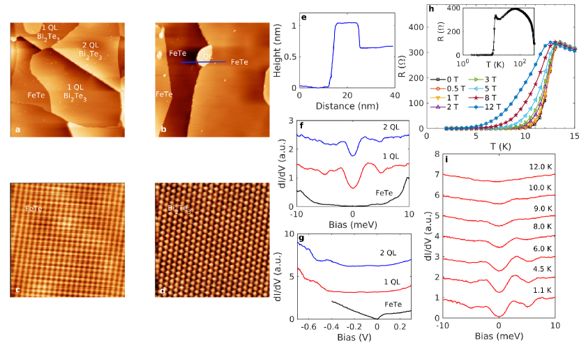
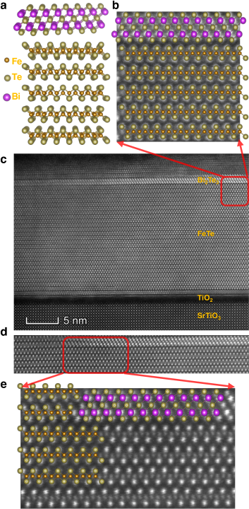
Fig. 1 (a) suggests a cross-sectional schematic illustration of 1 QL Bi2Te3 grown on FeTe, well matching the lattice of the red square indicated region(Fig. 1 (b)) shown in the HRSTEM Fig. 1 (c), evidencing an sharp vdW interface without lattice distortion or inter-diffusion. Furthermore, a typical lateral B2Te3-FeTe heterojunction near a FeTe atomic step is imaged in Fig. 1 (d) and 1 (e), demonstrating a step-flow epitaxy. It is worth mentioning that no interstitial Fe atoms were detected by a careful examining the FeTe lattice shown in Fig. 1 (c). Combining with the 1:1 ratio of Fe/Te revealed by chemical analysis(see supplementary materials), we assert that the FeTe film is of strict stoichiometry, similar as previous reported stoichiometric FeTe thin films grown by MBE with Te rich flux Li et al. (2016).
The STM studies were carried out on more than 20 samples and the results are repeatable and consistent. Fig. 2 (a) is a typical topographic image after growth of about 12 QL of Bi2Te3, inside which we acquire atomic-resolution images of exposed FeTe surface and 1 QL Bi2Te3 surface shown in Fig. 2 (c) and (d), respectively, representing a perfect lattice without any adatoms and vacancies being observed. The growth time for the sample in Fig. 2(b) was extremely short to observe the growth behavior, showing a nucleation of Bi2Te3 takes place on the atomic step of FeTe, consistent with cross-sectional HRSTEM results shown in Fig. 1. Fig. 2 (e) is the line profile corresponding to the blue line in Fig. 2 (b). The step height of about 0.6 nm and 1.0 nm correspond to one unit cell of FeTe and 1 QL layer of Bi2Te3, respectively. Representative spectra in a narrow bias range acquired on the FeTe, 1 QL Bi2Te3, and 2 QL Bi2Te3 terraces are shown in Fig. 2 (f). measures the local DOS near the Fermi level. The spectra acquired on the 1 QL Bi2Te3 terrace show two clear coherent superconducting peaks around 2.5 meV. This is in clear contrast to the spectrum acquired on the FeTe surface, which shows no coherent peaks, but a valley shape spectrum with a flat bottom. On the 2 QL Bi2Te3, the spectrum also exhibits two coherent superconducting peaks; however, the peaks are smaller at around 1.8 meV. The spectra on each terrace also vary little, indicating a good uniformity of the superconductivity. The temperature dependent spectra on the 1 QL Bi2Te3 surface are shown in Fig. 2 (i), while the results on the 2 QL are in the Supplementary Materials Not . While no significant change in the intensity of the coherence peak for the spectra is observed for temperature below 6 K, there is a significant decrease in the peak intensity at temperatures above 6 K. The gap magnitude is discernible up to about 10 K. At 12 K, there is no clear gap observed, consistent with followed transport revealed Tc. Typical spectra in a wider bias range obtained in the FeTe, 1 QL Bi2Te3, and 2 QL Bi2Te3 surfaces are plotted in Fig. 2 (g). According to the dI/dV spectrum Bi2Te3 film of 1 QL, there is discernibly weak and nearly constant density of states from 0 eV (Fermi level) to -0.43 eV. Below about -0.43 eV, the density of states start to rise rapidly with a kink at about -0.55 eV. On the Bi2Te3 film of 2 QL, there are two kinks around 0.08 eV and -0.44 eV, likely corresponding to the conduction band minimum (CBM) and valence band maximum (VBM), respectively. Comparing with the spectrum on the thick Bi2Te3 film Not , it indicates that the 1 QL Bi2Te3 film and 2 QL Bi2Te3 film are both more n-type doped. While this is qualitatively consistent with what is observed by Xu et al. Xu et al. (2015), the Fermi level shifts on the 1 QL and 2 QL Bi2Te3 are more significant, indicating the electron doping effect from the FeTe film likely plays an important role.
The temperature dependent in-plane resistance (- curve) of a Bi2Te3/FeTe/STO device with an average Bi2Te3 thickness of around 1 QL is shown in Fig. 2 (h). In the zero field (the inset in Fig. 2 (h)), a broad transition at about 65 K is observed, likely related to the magnetic and/or structural transition of FeTe films Bao et al. (2009); Li et al. (2009); Rößler et al. (2011); Rodriguez et al. (2011); Mizuguchi et al. (2012); Zaliznyak et al. (2012); Koz et al. (2013). The – curve shows a superconducting transition with an onset temperature of K and zero resistance temperature of K. Before , there is a upturn in - curve with decreasing temperature. The magnetic field (applied perpendicular to the sample interface) suppresses the superconductivity, and 12 T field is far away to completely kill the superconductivity, indicating a very high critical field, which is a characteristic feature of FeTe based superconductors Si et al. (2010).
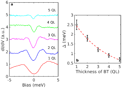
The spectra were acquired on samples with thicker Bi2Te3 films up to about 5-6 QL and are all shown in Fig. 3 (a). As can be seen, all of these spectra exhibit two coherent peaks, whereas the gap magnitude decreases with increasing Bi2Te3 thickness. The gap magnitude of the spectra is plotted in Fig. 3 (b) with respect to the number of QLs of Bi2Te3. The shows an exponential decay with a relationship of (in unit of meV, N is the number of QLs of Bi2Te3) as obtained from the fitting, consistent with the characteristic of proximity-induced superconductivity Xu et al. (2014), from which we can infer that the superconductivity is not enhanced in any way when the Bi2Te3 is 2 QLs or more than that when the Bi2Te3 is only 1 QL; instead, the superconductivity locates in the 1 QL Bi2Te3/FeTe interface, and becomes weaker on the Bi2Te3 surface due to the proximity effect.
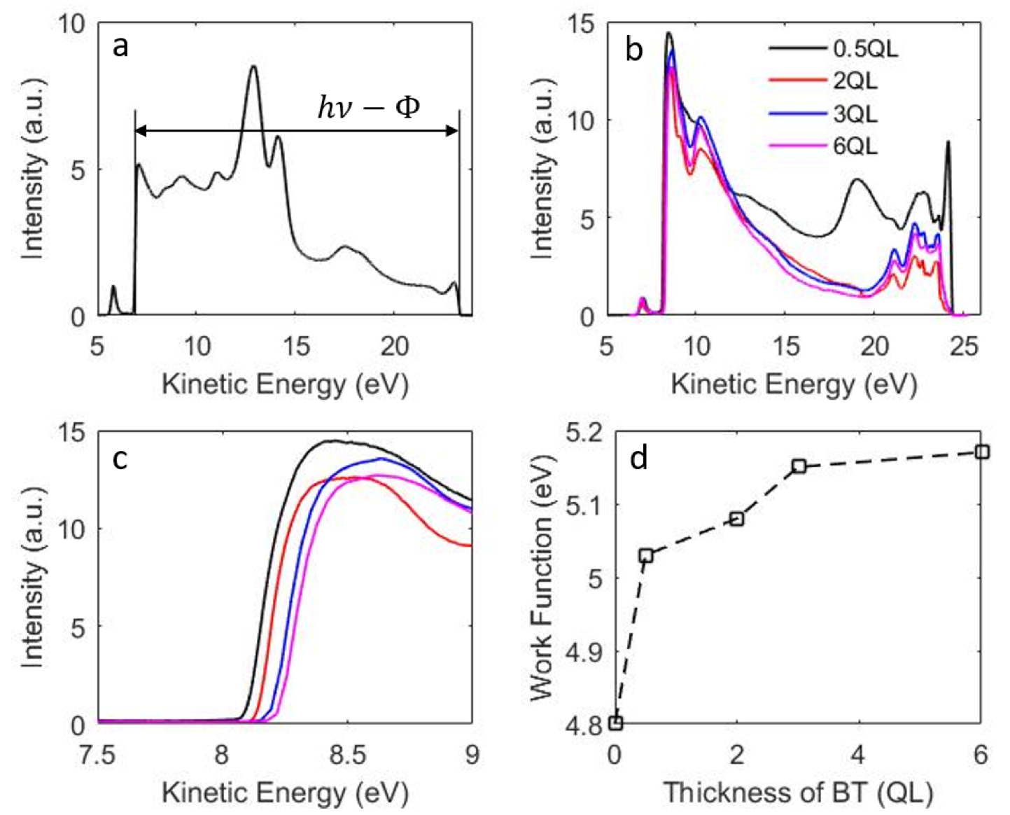
To further unveil the charge transfer mechanism between Bi2Te3 and FeTe, we also in-situ measured the work function of the FeTe film before and after the growing of Bi2Te3 film with average thickness of 0.5 QL, 2 QL, 3 QL, and 6 QL , respectively using UPS at 15 K. The UPS result of FeTe film is shown in Fig. 4 (a). A voltage -2 V was applied between the sample and the spectrometer so that the photoelectrons were accelerated and then the low energy inelastic electrons could be distinguished from secondary electrons generated in the spectrometer by impact Schlaf , which can be seen in Fig. 4 (a) as a small peak near 5.5 eV. The work function is calculated with the formula , where is the photon energy and is the spectrum width, the distance between the low energy cutoff and the Fermi edge as shown in Fig. 4 (a). Then we measured the photoemission spectrums of Bi2Te3 covered- FeTe with increasing thickness of Bi2Te3 and the results are shown in Fig. 4 (b). The zoom-in view of the low kinetic energy region of Fig. 4 (b) is shown in Fig. 4 (c), depicting that the inelastic edge offsets to the high kinetic energy region as the thickness of Bi2Te3 being increased, while the fermi edge in the high energy end is pinned in all the spectrums as they are determined by the accelerating voltage(- 3 V) solely. The extracted work functions are shown in Fig. 4 (d). As can be seen, the work function of FeTe film is about 4.80 eV. With the growth of Bi2Te3, the work function increases gradually, and starts to saturate when the Bi2Te3 thickness reaches about 3 QL. This result clearly suggests that there is a doping effect when the Bi2Te3 film is deposited onto the FeTe film, i.e., FeTe is hole-doped and Bi2Te3 film is electron-doped, qualitatively consistent the STS revealed charge transfer in Fig. 2 (g).
In the heterostructure of Bi2Te3/FeTe in our study, neither Bi2Te3 or FeTe is superconducting. Upon doping, Bi2Te3 is only superconducting with a maximum reported transition temperature of 5.5 K Hor et al. (2011). On the other hand, FeTe is superconducting upon doping with either oxygen Si et al. (2010) or selenium Fang et al. (2008) with a transition temperature of about 14 K, which is surprisingly close to the transition temperature in our study. Our work function measurements clearly show that there is a hole doping effect on the FeTe layer in the heterostructure. Therefore, it is plausible that the single FeTe layer become superconductivity due to the loss of electrons induced by Bi2Te3 covering, leading to the interface superconductivity observed in our study. While it still remains a challenge on how this doping leads to the observed superconductivity, our results provide more insights for future theoretic work to understand this doping induced change on electronic and magnetic properties of a single FeTe layer, which may also shed light on resolving the mystery of iron based superconductivity.
In conclusion, the superconductivity of Bi2Te3/FeTe system is studied by using the low temperature scanning tunneling microscopy. It is found that the superconductivity in the Bi2Te3/FeTe system can be induced by only one QL of Bi2Te3, which is also confirmed by the transport measurements. Scanning tunneling spectroscopy further shows that the superconducting gap decays exponentially with the increasing Bi2Te3 thickness, implying the superconductivity in Bi2Te3 bulk is actually proximity-induced by the interface. Our results provide unambiguous evidence that the superconductivity in the Bi2Te3/FeTe system is located around the Bi2Te3/FeTe interface. As for the superconducting mechanism, it is found that the doping of FeTe may be possible to generate superconductivity in the Bi2Te3/FeTe vdW hetero-junctions.
Acknowledgements.
We thanks H. H. Wen, L. Yu and P. A. Marchetti for discussions. This work was supported by the National Natural Science Foundation of China (NO. 61734008 and 11774143), the National Key Research and Development Program of China (No. 2018YFA0307100, No. 2016YFA0301703), the Natural Science Foundation of Guangdong Province (No. 2015A030313840, No. 2017A030313033), the State Key Laboratory of Low-Dimensional Quantum Physics (No. KF201602), Technology and Innovation Commission of Shenzhen Municipality ( ZDSYS20170303165926217 and JCYJ20170412152334605). J.W.M was partially supported by the program for Guangdong Introducing Innovative and Entrepreneurial Teams (No. 2017ZT07C062).References
- Ginzburg (1964) V. L. Ginzburg, “On surface superconductivity,” Physics Letters 13, 101–102 (1964).
- Miller et al. (1973) D. L. Miller, Myron Strongin, O. F. Kammerer, and B. G. Streetman, “Superconductivity at the surface of pbte,” Phys. Rev. B 8, 4416–4419 (1973).
- Ahn et al. (1999) C. H. Ahn, S. Gariglio, P. Paruch, T. Tybell, L. Antognazza, and J.-M. Triscone, “Electrostatic modulation of superconductivity in ultrathin gdba2cu3o7-x films,” Science 284, 1152–1155 (1999).
- Ahn et al. (2003) C. H. Ahn, J.-M. Triscone, and J. Mannhart, “Electric field effect in correlated oxide systems,” Nature 424, 1015 (2003).
- Reyren et al. (2007) N. Reyren, S. Thiel, A. D. Caviglia, L. Fitting Kourkoutis, G. Hammerl, C. Richter, C. W. Schneider, T. Kopp, A.-S. Rüetschi, D. Jaccard, M. Gabay, D. A. Muller, J.-M. Triscone, and J. Mannhart, “Superconducting interfaces between insulating oxides,” Science 317, 1196–1199 (2007).
- Gozar et al. (2008) A. Gozar, G. Logvenov, L. Fitting Kourkoutis, A. T. Bollinger, L. A. Giannuzzi, D. A. Muller, and I. Bozovic, “High-temperature interface superconductivity between metallic and insulating copper oxides,” Nature 455, 782 (2008).
- Pereiro et al. (2011) Juan Pereiro, Alexander Petrovic, Christos Panagopoulos, and Ivan Božović, “Interface superconductivity: History, development and prospects,” arXiv preprint arXiv:1111.4194 (2011).
- Wang et al. (2014) Gan Wang, Qing Lin He, Hong-Tao He, Hong-Chao Liu, Mingquan He, Jian-Nong Wang, Rolf Lortz, George Ke Lun Wong, and Iam Keong Sou, “Formation mechanism of superconducting fe1+xte/bi2te3 bilayer synthesized via interfacial chemical reactions,” Crystal Growth & Design 14, 3370–3374 (2014).
- He et al. (2014) Qing Lin He, Hongchao Liu, Mingquan He, Ying Hoi Lai, Hongtao He, Gan Wang, Kam Tuen Law, Rolf Lortz, Jiannong Wang, and Iam Keong Sou, “Two-dimensional superconductivity at the interface of a Bi2Te3/FeTe heterostructure,” Nature Communications 5, 4247 (2014).
- Zhang et al. (2018) Yi-Min Zhang, Jia-Qi Fan, Wen-Lin Wang, Ding Zhang, Lili Wang, Wei Li, Ke He, Can-Li Song, Xu-Cun Ma, and Qi-Kun Xue, “Observation of interface superconductivity in a /epitaxial graphene van der waals heterostructure,” Phys. Rev. B 98, 220508 (2018).
- Fogel et al. (1996) Nina Ya. Fogel, V. G. Cherkasova, A. S. Pokhila, A. Yu. Sipatov, and A. I. Fedorenko, “Superconductivity in the novel semiconducting superlattices,” Czechoslovak Journal of Physics 46, 727–728 (1996).
- Xu et al. (2014) Jin-Peng Xu, Canhua Liu, Mei-Xiao Wang, Jianfeng Ge, Zhi-Long Liu, Xiaojun Yang, Yan Chen, Ying Liu, Zhu-An Xu, Chun-Lei Gao, Dong Qian, Fu-Chun Zhang, and Jin-Feng Jia, “Artificial topological superconductor by the proximity effect,” Phys. Rev. Lett. 112, 217001 (2014).
- Koma (1992) Atsushi Koma, “Van der waals epitaxy—a new epitaxial growth method for a highly lattice-mismatched system,” Thin Solid Films 216, 72 – 76 (1992).
- Bao et al. (2009) Wei Bao, Y. Qiu, Q. Huang, M. A. Green, P. Zajdel, M. R. Fitzsimmons, M. Zhernenkov, S. Chang, Minghu Fang, B. Qian, E. K. Vehstedt, Jinhu Yang, H. M. Pham, L. Spinu, and Z. Q. Mao, “Tunable (, )-type antiferromagnetic order in -fe(te,se) superconductors,” Phys. Rev. Lett. 102, 247001 (2009).
- Xia et al. (2009) Y. Xia, D. Qian, L. Wray, D. Hsieh, G. F. Chen, J. L. Luo, N. L. Wang, and M. Z. Hasan, “Fermi surface topology and low-lying quasiparticle dynamics of parent superconductor,” Phys. Rev. Lett. 103, 037002 (2009).
- Du et al. (2015) Guan Du, Zengyi Du, Xiong Yang, Enyu Wang, Delong Fang, Huan Yang, and Hai-Hu Wen, “Merging dirac electrons and correlation effect in the heterostructured bi2te3/fe1+ dte,” arXiv preprint arXiv:1509.07424 (2015).
- Kunchur et al. (2015) M. N. Kunchur, C. L. Dean, N. Shayesteh Moghadam, J. M. Knight, Q. L. He, H. Liu, J. Wang, R. Lortz, I. K. Sou, and A. Gurevich, “Current-induced depairing in the interfacial superconductor,” Phys. Rev. B 92, 094502 (2015).
- Manna et al. (2017) Sujit Manna, Anand Kamlapure, Lasse Cornils, Torben Hänke, Ellen Marie Jensen Hedegaard, Martin Bremholm, Bo Brummerstedt Iversen, Ph Hofmann, Jens Wiebe, and Roland Wiesendanger, “Interfacial superconductivity in a bi-collinear antiferromagnetically ordered fete monolayer on a topological insulator,” Nature communications 8, 14074 (2017).
- Arnold et al. (2018) Fabian Arnold, Jonas Warmuth, Matteo Michiardi, Jan Fikáček, Marco Bianchi, Jin Hu, Zhiqiang Mao, Jill Miwa, Udai Raj Singh, Martin Bremholm, Roland Wiesendanger, Jan Honolka, Tim Wehling, Jens Wiebe, and Philip Hofmann, “Electronic structure of fe 1.08 te bulk crystals and epitaxial fete thin films on bi 2 te 3,” Journal of Physics: Condensed Matter 30, 065502 (2018).
- Singh et al. (2018) Udai Raj Singh, Jonas Warmuth, Anand Kamlapure, Lasse Cornils, Martin Bremholm, Philip Hofmann, Jens Wiebe, and Roland Wiesendanger, “Enhanced spin-ordering temperature in ultrathin fete films grown on a topological insulator,” Phys. Rev. B 97, 144513 (2018).
- Li et al. (2016) Wei Li, Wei-Guo Yin, Lili Wang, Ke He, Xucun Ma, Qi-Kun Xue, and Xi Chen, “Charge ordering in stoichiometric fete: Scanning tunneling microscopy and spectroscopy,” Phys. Rev. B 93, 041101 (2016).
- (22) Hello world.
- Xu et al. (2015) Jin-Peng Xu, Mei-Xiao Wang, Zhi Long Liu, Jian-Feng Ge, Xiaojun Yang, Canhua Liu, Zhu An Xu, Dandan Guan, Chun Lei Gao, Dong Qian, Ying Liu, Qiang-Hua Wang, Fu-Chun Zhang, Qi-Kun Xue, and Jin-Feng Jia, “Experimental detection of a majorana mode in the core of a magnetic vortex inside a topological insulator-superconductor heterostructure,” Phys. Rev. Lett. 114, 017001 (2015).
- Li et al. (2009) Shiliang Li, Clarina de la Cruz, Q. Huang, Y. Chen, J. W. Lynn, Jiangping Hu, Yi-Lin Huang, Fong-Chi Hsu, Kuo-Wei Yeh, Maw-Kuen Wu, and Pengcheng Dai, “First-order magnetic and structural phase transitions in ,” Phys. Rev. B 79, 054503 (2009).
- Rößler et al. (2011) S. Rößler, Dona Cherian, W. Lorenz, M. Doerr, C. Koz, C. Curfs, Yu. Prots, U. K. Rößler, U. Schwarz, Suja Elizabeth, and S. Wirth, “First-order structural transition in the magnetically ordered phase of fe1.13te,” Phys. Rev. B 84, 174506 (2011).
- Rodriguez et al. (2011) E. E. Rodriguez, C. Stock, P. Zajdel, K. L. Krycka, C. F. Majkrzak, P. Zavalij, and M. A. Green, “Magnetic-crystallographic phase diagram of the superconducting parent compound fe1+xte,” Phys. Rev. B 84, 064403 (2011).
- Mizuguchi et al. (2012) Yoshikazu Mizuguchi, Kentaro Hamada, Kazuki Goto, Hiroshi Takatsu, Hiroaki Kadowaki, and Osuke Miura, “Evolution of two-step structural phase transition in fe1+dte detected by low-temperature x-ray diffraction,” Solid State Communications 152, 1047 – 1051 (2012).
- Zaliznyak et al. (2012) I. A. Zaliznyak, Z. J. Xu, J. S. Wen, J. M. Tranquada, G. D. Gu, V. Solovyov, V. N. Glazkov, A. I. Zheludev, V. O. Garlea, and M. B. Stone, “Continuous magnetic and structural phase transitions in fe1+yte,” Phys. Rev. B 85, 085105 (2012).
- Koz et al. (2013) Cevriye Koz, Sahana Rößler, Alexander A. Tsirlin, Steffen Wirth, and Ulrich Schwarz, “Low-temperature phase diagram of fe1+yte studied using x-ray diffraction,” Phys. Rev. B 88, 094509 (2013).
- Si et al. (2010) Weidong Si, Qing Jie, Lijun Wu, Juan Zhou, Genda Gu, P. D. Johnson, and Qiang Li, “Superconductivity in epitaxial thin films of ,” Phys. Rev. B 81, 092506 (2010).
- (31) Rudy Schlaf, “Calibration of photoemission spectra and work function determination,” http://rsl.eng.usf.edu/Documents/Tutorials/ PEScalibration.pdf .
- Hor et al. (2011) Y.S. Hor, J.G. Checkelsky, D. Qu, N.P. Ong, and R.J. Cava, “Superconductivity and non-metallicity induced by doping the topological insulators bi2se3 and bi2te3,” Journal of Physics and Chemistry of Solids 72, 572 – 576 (2011), spectroscopies in Novel Superconductors 2010.
- Fang et al. (2008) M. H. Fang, H. M. Pham, B. Qian, T. J. Liu, E. K. Vehstedt, Y. Liu, L. Spinu, and Z. Q. Mao, “Superconductivity close to magnetic instability in ,” Phys. Rev. B 78, 224503 (2008).