Macroscopically Aligned Carbon Nanotubes as a Refractory Platform for Hyperbolic Thermal Emitters
Abstract
Refractory nanophotonics, or nanophotonics at high temperatures, can revolutionize many applications, including data storage and waste heat recovery. In particular, nanophotonic devices made from hyperbolic materials are promising due to their nearly infinite photonic density of states (PDOS). However, it is challenging to achieve a prominent PDOS in existing refractory hyperbolic materials, especially in a broad spectral range. Here, we demonstrate that macroscopic films and architectures of aligned carbon nanotubes work as excellent refractory hyperbolic materials. We found that aligned carbon nanotubes are thermally stable up to and exhibit extreme anisotropy — metallic in one direction and insulating in the other two directions. Such extreme anisotropy makes this system a hyperbolic material with an exceptionally large PDOS over a broadband spectrum range (longer than m) in the midinfrared, exhibiting strong resonances in deeply sub-wavelength-sized cavities. We observed polarized, spectrally selective thermal emission from aligned carbon nanotube films as well as indefinite cavities of aligned carbon nanotubes with volume as small as operating at . These experiments suggest that aligned carbon nanotubes possess naturally large PDOS that leads to thermal photon densities enhanced by over two orders of magnitude, making them a promising refractory nanophotonics platform.
Nanophotonics at high temperatures is an emerging technology that enables many new applications. For example, thermophotovoltaic energy conversion, useful for waste heat recovery, can be significantly more efficient with mid-infrared refractory nanophotonic devices Coutts and Fitzgerald (1998); Basu et al. (2007); Kraemer et al. (2011); Lenert et al. (2014). Given that the waste heat accounts for 67% of all energy used in direct energy production in the United States ene (2017) alone, refractory nanophotonics can change the landscape of future energy technology. Additionally, refractory nanophotonics enables novel infrared sources Greffet et al. (2002); Schuller et al. (2009); Liu et al. (2011, 2015); Costantini et al. (2015); Dyachenko et al. (2016); Ilic et al. (2016), ultrahigh density data storage Challener et al. (2009); Stipe et al. (2010), and innovative chemical sensing techniques Inoue et al. (2013); Lochbaum et al. (2017). In particular, refractory hyperbolic devices possessing huge PDOS hold great promise in sculpting the flow of thermal radiation Jacob et al. (2012); Drachev et al. (2013); Poddubny et al. (2013); Shekhar et al. (2014), especially in the near-field where the radiative heat transfer can be enhanced beyond Planck’s law by several orders of magnitude Biehs et al. (2012); Guo et al. (2012); Guo and Jacob (2013); Liu et al. (2013); Zhao et al. (2017); Fiorino et al. (2018). Although natural hyperbolic materials are better in terms of PDOS enhancement than artificial ones, the state-of-the-art refractory hyperbolic material choices suffer from narrow bandwidth and lack of short infrared operation. For example, thermally stable hexagonal form boron nitride (h-BN) and silicon carbide can support hyperbolic dispersions, but only in narrow ranges in 6-12 m spectral window Shekhar et al. (2014); Caldwell et al. (2014); Dai et al. (2014); Yoxall et al. (2015); Tamagnone et al. (2018). Layered graphite possesses hyperbolic dispersions in either ultraviolet range or long infrared wavelength range ( m). Cuprates and ruthenates Sun et al. (2014) supporting broadband hyperbolic dispersions face nanofabrication challenges, and it is not clear whether or not these are refractory materials. Addressing the lack of good refractory hyperbolic materials, here we demonstrate aligned films of single-wall carbon nanotubes (SWCNTs) as an ideal broadband natural hyperbolic refractory material platform for thermal radiation engineering across the mid-infrared.
SWCNTs are one-dimensional materials possessing unique properties, and hence are promising for applications including nanoelectronics and optoelectronics Avouris et al. (2007, 2008). In particular, the strong quantum confinement results in extremely anisotropic electronic, optical and thermal properties Dresselhaus et al. (2001), making them exceptional for thermal radiation engineering. To preserve these extraordinary properties at nanoscale in large-scale device applications requires a fabrication technique of producing ensembles of SWCNTs with macroscopic alignment, high packing density, controllable metallicity and chirality, and compatibility with facile nano/micromanufacturing, but it had been a grand challenge of developing successful methods. Recently, we developed a versatile vacuum filtration technique to prepare such aligned SWCNT films He et al. (2016), paving the way for highly anisotropic thermal emitters.
A closely packed bundle of aligned metallic or doped semiconducting SWCNTs can be described by a uniaxial anisotropic medium with effective permittivities and along the tube axis and in the perpendicular plane, respectively. The conductivity due to free carriers along the nanotubes causes a metallic optical response, leading to Re. In contrast, the nanotubes are insulating in the perpendicular plane, leading to Re. This extreme anisotropy leads to a broadband hyperbolic dispersion, which spans a majority of the mid-infrared range, a significant portion of the spectrum of interest for selective thermal emitters. The enhancement of PDOS in hyperbolic materials is limited by the geometry of the material, i.e., the validity limit of the effective medium approximation for high momentum photons (high-k modes) Guo et al. (2012); Guo and Jacob (2013). However, because of the extremely small diameters of SWCNTs (1 nm) compared to the infrared wavelengths, highly aligned and densely packed SWCNT films can support much higher k modes, enabling over 1000 enhancement in PDOS. Because of their hyperbolic dispersions and ultrahigh chemical stability up to 1600 Yudasaka et al. (2001), SWCNTs provide a promising platform for mid-infrared refractory nanophotonics and thermal radiation engineering Molesky and Jacob (2015).
Here, we report hyperbolic thermal emitters emitting spectrally selective and polarized mid-infrared radiation with a 700 operating temperature. This novel emitter is based on highly aligned and densely packed SWCNTs prepared through spontaneous alignment that occurs during vacuum filtration He et al. (2016). In comparison to vertically aligned SWCNTs grown by the chemical-vapor-deposition (CVD) methodMurakami et al. (2004), our films have a significantly higher packing density, sustain high temperatures, and are robust during nanofabrication. We demonstrate that aligned SWCNT films have a hyperbolic dispersion at wavelengths longer than 4.3 m ( cm-1) at 700 . In direct thermal emission measurements, we observed strongly polarized and narrowband radiation from aligned SWCNT thin films originating from the Berreman modes excited near the epsilon-near-zero (ENZ) frequency. Furthermore, we demonstrate propagating high-k photons in the hyperbolic medium, enabling enhanced thermal emission in deep sub-wavelength cavities of volume , where is the resonance wavelength. The thermal emission is widely tunable in the mid-infrared range by adjusting the dimensions of the aligned SWCNT structures.
In order to demonstrate unique optical and thermal radiation properties of the aligned SWCNT structures, we measured their thermal emission and reflectivity at temperatures up to 700 using a Fourier transform infrared (FTIR) spectrometer, equipped with a reflective microscope and a heated vacuum stage (see Figure 1a). See Materials and Methods for more details of the experimental setup. Macroscopically aligned, densely packed SWCNT films were prepared by filtrating a well-dispersed SWCNT suspension through a 2-inch filtration system He et al. (2016); Komatsu et al. (2017). The as-prepared films contained both metallic and semiconducting nanotubes with an average diameter of 1.4 nm. The obtained films were well aligned and densely packed, as observed in the scanning electron micrograph of Figure 1b and the cross-sectional transmission electron micrograph in the inset of Figure 1b. The SWCNT films were transferred onto different substrates using a standard wet transfer technique He et al. (2016). We further fabricated indefinite cavities using electron beam lithography and reactive ion etching. See Materials and Methods and Supplementary Figure S1 for the details of the wet transfer and nanofabrication processes, and additional sample characterization data.
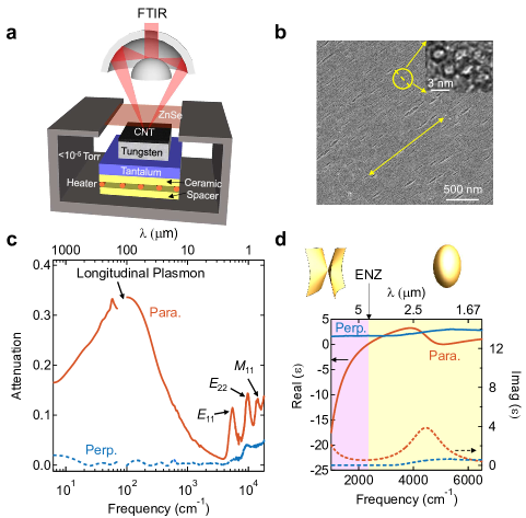
A room-temperature optical absorption spectrum for a densely packed aligned SWCNT film in a broad spectral range is shown in Figure 1c, from terahertz (THz) to visible, obtained using THz time-domain spectroscopy, FTIR, and visible-near-IR spectroscopy. The optical absorption is strongly polarization dependent. When the polarization is perpendicular to the tube axis, the absorption is small and featureless. On the other hand, a prominent absorption peak at cm-1 is observed for the parallel polarization case arising from the longitudinal plasmon resonance Zhang et al. (2013) in finite-length SWCNTs. Further, absorption peaks in the near-infrared and visible ranges, arising from the first two interband transitions for semiconducting tubes ( and ) and the first interband transition for metallic tubes () are clearly observed in the parallel polarization case.
Wavelength-dependent dielectric constants of the SWCNT films in both directions ( and ) were extracted from reflectance measurements at room temperature and 700 . A combination of Drude and Lorentz oscillators Zhang et al. (2013) were used to retrieve the dielectric function in the parallel direction, and a point-wise retrieval Denton et al. (1972) was employed for the perpendicular case (see SI for more information). At room temperature, the aligned SWCNT film have a hyperbolic dispersion below 3300 cm-1 ( m). The room temperature dielectric constants are reported in Supplementary Figure S2c. At 700 , the extracted dielectric functions are very similar to the room temperature measurements except for increased Drude damping and a slight red-shift in the plasma frequency at 700 . The red-shift in the plasma frequency can be attributed to high-temperature-induced dedoping Wu et al. (2004). However, the optical properties of aligned SWCNTs remained stable under vacuum after dedoping during the first heating cycle. Reflectivity measurements during heating cycles are discussed in Supplementary Note 1 and Figure S2.
Figure 1d shows the real and imaginary parts of the extracted ordinary and extraordinary dielectric constants in both directions at 700 . The permittivity perpendicular to the tube axis shows a low-loss dielectric behavior over the whole spectral range (Re() 0, Im() 0), whereas the permittivity parallel to the tube axis is metallic (Re() in the mid-infrared with an ENZ frequency of about 2335 cm-1 (4.3 m). While the real permittivities have different signs in different directions for frequencies smaller than the ENZ frequency, they are both positive for higher frequencies. The extreme anisotropy for frequencies smaller than the ENZ frequency results in a hyperbolic dispersion or hyperboloid isofrequency surface, an open surface with an unbounded surface area and hence an unbounded PDOS Jacob et al. (2012). The nearly infinite PDOS of hyperbolic materials arising from the allowed propagation of extremely high-momentum (high-k) waves has many consequences in the context of thermal radiation, including super-Planckian thermal emission, significantly enhanced near-field radiative heat transfer, and thermal conductivity beyond the Stephan-Boltzmann law Guo et al. (2012); Narimanov and Smolyaninov (2012). The aligned SWCNT film supports a hyperbolic dispersion below 2335 cm-1 ( m) at 700 , covering a significant portion of the region of interest for selective thermal emitters.
To demonstrate the hyperbolic behavior of aligned SWCNT films, we first characterized the thermal emission from continuous films. The frequency at which the dispersion goes from ellipsoidal to hyperbolic is the ENZ frequency, where we would expect the maximum thermal emission from continuous films Guo et al. (2012). Thermal emission measurements of continuous films of aligned SWCNTs on tungsten substrates at 700 are shown in Figure 2. Figure 2a shows polarization-dependent thermal emission from two different SWCNT films with thicknesses of 188 nm and 1.75 m, respectively. All emission spectra are normalized with respect to the relatively flat emission spectrum of the tungsten substrate. In the case of the thinner film (188 nm), we clearly observe a prominent emission peak denoted as in the parallel polarization, whereas no such peak is observed in the perpendicular polarization. The peak originates from the impedance matching condition in the multilayer structure, leading to the excitation of Berreman modes Harbecke et al. (1985). Since no such phenomenon occurs in the perpendicular polarization, we do not see any enhanced thermal emission. The polarization dependence of the thermal emission from the 188 nm-thick film is shown in Figure 2b. The experimental data can be fit with a curve very well, which is also consistent with the polarization-dependent absorptivity in aligned SWCNTs Murakami et al. (2005). A contrast over three in emission intensity is observed between the two orthogonal polarizations.
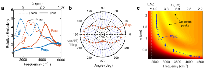
Figure 2c shows calculated emission spectra for various film thicknesses based on the transfer matrix method (hot colormap mapping), and the peak seen in experiments (blue dots connected by a dashed line). As the SWCNT film thickness increases, red-shifts to asymptotically approach the ENZ frequency. Thicker films also support Fabry-Perot resonances, leading to several dielectric peaks in both parallel and perpendicular polarizations, as seen in Figures 2a and 2c. Thicker samples were fabricated via a manual stacking technique developed recently (see Materials and Methods for more details) Komatsu et al. (2017). The experimental peak matches well with calculations. We clearly observe that approaches the ENZ frequency (white dashed line) when the film thickness increases, as shown in Figure 2c. The increasing error bars for thicker films are from the cumulative thickness uncertainty in the transfer process. Note that the influence of fabrication imperfections, including imperfect conformal transfer and small misalignment between layers, is expected to be negligible on thermal emission because the standard deviation in the angle of alignment of SWCNT films was found out to be less than two degrees He et al. (2016). The stacking technique can indeed preserve alignment between layers very well and stack films consistently Komatsu et al. (2017).
Extremely large PDOS for hyperbolic materials implies that the medium can support a significantly larger number of thermal photons per unit volume than a blackbody. In other words, a hyperbolic medium can support the same number of thermal photons as a blackbody in a much smaller volume. However, not all of these thermal photons radiate out to far-field because of momentum mismatch. Nanostructuring hyperbolic materials can resonantly outcouple some of these photons and provide information about their momentum. Thus, observing resonances in far-field thermal emission from sub-wavelength cavities of hyperbolic or indefinite materials allows probing the momentum of high- thermal photons supported by the medium Yao et al. (2011); Yang et al. (2012). Figure 3 summarizes finite-difference-time-domain (FDTD) simulation results of SWCNT indefinite cavities. We considered a square lattice of SWCNT indefinite cavities on a tungsten substrate with a 400-nm-thick Al2O3 spacer as shown in the schematic of Figure 3a. The 400-nm-thick Al2O3 spacer reduces any plasmonic interaction between the cavities and the tungsten substrate. We included a 50-nm-thick SiO2 layer on top of SWCNTs, which served as an etch mask during fabrication. The array period and the thickness of the SWCNT layer were fixed at 2.5 m and 500 nm, respectively. The lengths of the cavity in directions parallel and perpendicular to the tube axis are denoted by and , respectively. Invoking Kirchoff’s law, we calculated the emissivity spectra for various and combinations. Figure 3b shows the calculated emissivity relative to the tungsten substrate as a function of frequency for indefinite cavities with various and constant at 1.05 m. An emissivity peak is observed only in polarization parallel to the tube axis and originates from the hyperbolic resonance in the deep sub-wavelength cavities. The resonance red-shifts with increasing as expected in any plasmonic or photonic structures.

However, indefinite cavities differ from conventional plasmonic or photonic cavities in that their resonance scales anomalously with and Yao et al. (2011); Yang et al. (2012) as demonstrated in Figure 3c. Here, we designed three cavities with different combinations of and in such a way that the emissivity peak occurs at the same frequency. The dimensions of the three cavities chosen in Figure 3c are indicated in the parentheses as (, ) in m. Note that , scale the same way unlike in conventional cavities to keep the resonance at the same position. Also, all of these cavities are deeply subwavelength and support the same TM11 resonance. Figure 3d shows the resonant electric field () distribution for the smallest cavity (see Supplementary Figure S3 for more data). Unlike plasmonic resonators, the field inside an indefinite cavity is enhanced similar to a photonic resonance. Since the optical losses that lead to thermal radiation are present primarily inside the cavity, the field enhancement effectively leads to enhanced thermal radiation. The divergence of the Poynting vector presented in Figures S3a-c shows the location where thermal emission originates.
We fabricated an array of indefinite cavities; false-color scanning electron micrographs are shown in Figure 4a. The inset shows the SiO2 mask, 500-nm thick patterned CNT cavities, and the 400-nm thick Al2O3 film on the tungsten substrate. Figure 4b shows measured relative thermal emission spectra from indefinite cavities with a fixed of 1.5 m and three different values of . The emissivity peaks red-shift with increasing , in qualitative agreement with the simulations results shown in Figure 3b. Increasing while fixing results in a blue-shift; see Supplementary Note 2 and Figure S4.
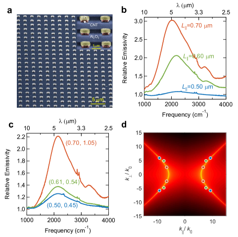
By simultaneously changing and , we can maintain the resonance frequency at a single frequency, as shown in Figure 4c. For all three different (, ) combinations, the cavities emit resonantly at 2140 cm-1 (4.7 m). This emission peak is slightly blue-shifted from the simulations and is also broader largely due to fabrication imperfections. By tuning the dimensions of the cavities so that the resonances trace an isofrequency contour, the dispersion of the SWCNT layer can be determined at this frequency. Figure 4d plots the experimentally measured dispersion points on the isofrequency contour of the SWCNT film calculated from the previously measured dielectric constants of the SWCNT film at 2140 cm-1. Here, is the wavevector component along the tube alignment direction (-axis), is that perpendicular to the alignment direction in the film plane (-axis), and is the wavenumber in vacuum. The measured dispersion agrees well with the calculations, confirming the existence of a hyperbolic dispersion behind the observed thermal emission behaviors. Further, the observation of resonances in deep sub-wavelength sized cavities proves that high-k waves supported in the SWCNT hyperbolic medium lead to significantly high PDOS or density of thermal photons. The smallest cavity in which we observed a resonance had a volume of , indicating at least a 100 enhancement of PDOS in SWCNT hyperbolic thermal emitters.
We demonstrated that aligned SWCNTs make an excellent material platform for refractory nanophotonics in the mid-infrared. Our aligned SWCNT devices showed broadly tunable, polarized, and spectrally selective hyperbolic thermal emitters operating at 700 . While thin films of aligned SWCNTs exhibited enhanced thermal emission near their ENZ frequency due to the excitation of Berreman modes, nanopatterned films showed geometry-tunable spectrally-selective thermal emission arising from indefinite cavity resonances. These resonances in deep sub-wavelength cavities allowed direct measurements of hyperbolic dispersions in SWCNT films, proving the existence of propagating high-k waves and significantly large PDOS. Photonic-like resonances in cavities of volume as small as showed that the density of thermal photons in the SWCNT hyperbolic medium is greater than that in a blackbody by at least 100.
I Methods
I.1 Thermal emission and reflectivity experimental setup
A Thermo Fisher Scientific Fourier transform infrared (FTIR) spectrometer, equipped with a microscope and a customized high-vacuum PID-controlled heating element, was used to measure the thermal emission and reflectivity of aligned SWCNT structures. The microscope has a reflective infrared objective, with NA = 0.24 (corresponding to a collection angle ) and aperture size 300 m 300 m. A zinc selenide (ZnSe) window with anti-reflection coating was mounted on the heating stage for the light collection in the whole mid-infrared region, from 1000 cm-1 to 7000 cm-1. The heating element consists of a resistive heater surrounded by ceramic spacers. A tantalum film was used to support samples and block the direct thermal emission from the heater. The heating element was kept at target temperatures for at least 30 minutes to reach thermal equilibrium before any measurements. All experiments were performed under high vacuum 10-5 Torr.
I.2 SWNCT sample preparation and indefinite cavity fabrication
Arc-discharge P2-SWCNTs with an average diameter 1.4 nm were purchased from Carbon Solutions, Inc. 20 mL 0.5% (wt./vol.) sodium deoxycholate (DOC, Sigma-Aldrich) was used to disperse 8 mg P2-SWCNTs. A tip sonicator was used to homogenize the suspension for 45 minutes, and the obtained suspension was ultracentrifuged for 1.5 hours at 38000 rpm to remove undispersed large bundles and impurities. Well-dispersed supernatant was collected, and then diluted to reduce the surfactant concentration below the critical michelle concentration (CMC) of DOC, which is considered to be a necessary condition for spontaneous alignment. The diluted suspension was then poured into a 2-inch vacuum filtration system to have a uniform, aligned, and densely packed SWCNT film. The obtained film can be transfered to various substrates, by dissolving the filter membrane in chloroform and then rinsing the sample in acetone He et al. (2016). Furthermore, multiple thin aligned films were stacked to have a thicker film by manually transferring several pieces onto the substrate one by one, while preserving the alignment direction Komatsu et al. (2017).
A 400-nm thick film of Al2O3 was deposited onto a tungsten substrate in an reaction of trimethylaluminum and water using an atomic layer deposition system. A thick film of aligned SWCNTs was transferred onto the Al2O3 film using the aforementioned stacking process. A 50-nm thick film of SiO2 was deposited onto the stacked SWCNT film as a hard mask, using an ultrahigh vacuum DC sputtering system. This hard mask aims to increase the dry etching selectivity for SWCNT patterning. We used standard electron beam lithography to define large-area patterns. A SU-8 positive lithography resist was deposited, following the coating of a thin layer of Omnicoat for easy lift-off. The patterns were first transferred onto the SiO2 hard mask using a sulfur hexafluoride (SF6) based reactive ion etching (RIE), and the SU-8 resist was removed using PG remover. Finally, a pure oxygen RIE was performed to transfer the patterns onto SWCNTs to form indefinite cavities.
II Supplementary Information
II.1 Reflectance spectra fitting and stability of aligned SWCNTs at 700 ∘C
A 110-nm thick film of aligned SWCNTs was transferred onto a CaF2 substrate for reflectance measurements. We used a Bruker Multimode 8 atomic force microscope (AFM) to determine the thickness of CNT films. Figure S1 demonstrates an AFM image (Figure S1a) of a single-layer film with thickness 42 nm 4 nm (Figure S1b).

The reflected signal from SWCNTs on a CaF2 substrate was normalized to the reflected signal from the CaF2 substrate. Along the tube alignment direction, the dielectric constant is modeled as
| (1) |
where captures the response from intertube transport and percolating channels in the macroscopic scale, characterizes the response from the confined collective motion in the tube-length level, and describes the first exciton peak. has a Drude response as
| (2) |
while and have Lorentzian shapes as
| (3) |
| (4) |
where , , , , , , , and are treated as fitting parameters. We calculated the reflectance from transfer matrix method (see next section), and fitted the whole spectrum simultaneously. The fitted spectra agrees well with the experimental result as shown in Figure S2a. Along the direction that is perpendicular to the tube alignment direction, the dielectric constant is modeled as a frequency-dependent complex number . We fitted the spectra point-by-point for each frequency. The following three points ensured that the recovered dielectric constants are unique and reliable: (i) the film thickness is not a fitting parameter and determined by atomic force microscopy. (ii) The Drude and Lorentz models used in the parallel direction connect real and imaginary parts through Kramers-Kronig relation. (iii) The dielectric constants in the perpendicular direction have negligible imaginary parts since the absorption is small.
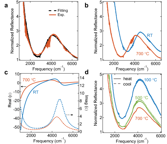
In addition, we compare the reflectance spectra and extracted dielectric constants along the tube alignment direction at room temperature and 700 for the first heating cycle. We clearly observe the spectra redshift in Figure S2b and the reduction of metallicity in Figure S2c at higher temperature. We attribute these behaviors to the SWCNT dedoping, as adsorbed water and gas molecules are removed from SWCNTs at 700 and under high vacuum. Once SWCNTs are dedoped, the optical properties of SWCNTS are very stable at high temperature and we do not see any noticeable change during the measurement, which usually lasted for tens of hours. Furthermore, we measured the reflectance spectra for more thermal cycles, and they agree well between the heating half-cycle and cooling half-cycle, as shown in Figure S2d.
II.2 Additional data on SWCNT hyperbolic cavities
Figure S3 summarizes the mappings of the divergence of Poynting vector (Figures S3a–c and field distribution (Figures S3d–f) for (0.56,0.38), (0.63, 0.58) and (0.70, 1.05) cavities, respectively, and field distribution (Figures S3h and S3h) for (0.63, 0.58) and (0.70, 1.05) cavities, respectively. All three cavities shown in Figure 3c of the main text support identical optical modes, and thermal emission is entirely from SWCNT cavities. We demonstrated hyperbolic cavities on the same isofrequency contour theoretically in Figure 3c of the main text and experimentally in Figures 4c and 4d, as we tuned and simultaneously.

Figures S4 shows the calculated (Figure S4a) and experimental (Figure S4b) emission spectra for cavities with only one adjustable parameter . In the hyperbolic region, the dielectric constant tensor of SWCNTs can be expressed as , where and . The isofrequency contour is described as
| (5) |
where are wavevectors along axes. As increases ( decreases) with , we observe a normal scaling leading to a redshift ( decreases in Fig. 3b of the main text). On contrary, as increases ( decreases and is fixed) with , we observe an anomalous scaling leading to a blueshift ( increases in Fig. S4). All these behaviors are consistent with the properties of hyperbolic cavities.

Acknowledgments. W. G. and C. D. contributed equally to this work. W. G., X. L., J. K. acknowledge support by the Basic Energy Science (BES) program of the US Department of Energy through grant no. DE-FG02-06ER46308 (for preparation of aligned carbon nanotube films), the US National Science Foundation through grant no. ECCS-1708315 (for optical measurements), and the Robert A. Welch Foundation through grant no. C-1509 (for structural characterization measurements).
References
- Coutts and Fitzgerald (1998) T. J. Coutts and M. C. Fitzgerald, Sci. Amer. 279, 90 (1998).
- Basu et al. (2007) S. Basu, Y.-B. Chen, and Z. Zhang, Int. J. Energy Res. 31, 689 (2007).
- Kraemer et al. (2011) D. Kraemer, B. Poudel, H.-P. Feng, J. C. Caylor, B. Yu, X. Yan, Y. Ma, X. Wang, D. Wang, A. Muto, et al., Nat. Mater. 10, 532 (2011).
- Lenert et al. (2014) A. Lenert, D. M. Bierman, Y. Nam, W. R. Chan, I. Celanović, M. Soljačić, and E. N. Wang, Nat. Nanotechnol. 9, 126 (2014).
- ene (2017) (2017), estimated U.S. Energy Consumption in 2017: 97.7 Quads, Lawrence Livermore National Laboratory. [Online]. Available at https://flowcharts.llnl.gov/commodities/energy.
- Greffet et al. (2002) J.-J. Greffet, R. Carminati, K. Joulain, J.-P. Mulet, S. Mainguy, and Y. Chen, Nature 416, 61 (2002).
- Schuller et al. (2009) J. A. Schuller, T. Taubner, and M. L. Brongersma, Nat. Photonics 3, 658 (2009).
- Liu et al. (2011) X. Liu, T. Tyler, T. Starr, A. F. Starr, N. M. Jokerst, and W. J. Padilla, Phys. Rev. Lett. 107, 045901 (2011).
- Liu et al. (2015) J. Liu, U. Guler, A. Lagutchev, A. Kildishev, O. Malis, A. Boltasseva, and V. M. Shalaev, Optical Materials Express 5, 2721 (2015).
- Costantini et al. (2015) D. Costantini, A. Lefebvre, A.-L. Coutrot, I. Moldovan-Doyen, J.-P. Hugonin, S. Boutami, F. Marquier, H. Benisty, and J.-J. Greffet, Phys. Rev. Appl 4, 014023 (2015).
- Dyachenko et al. (2016) P. Dyachenko, S. Molesky, A. Y. Petrov, M. Störmer, T. Krekeler, S. Lang, M. Ritter, Z. Jacob, and M. Eich, Nat. Commun. 7 (2016).
- Ilic et al. (2016) O. Ilic, P. Bermel, G. Chen, J. D. Joannopoulos, I. Celanovic, and M. Soljačić, Nat. Nanotechnol. 11, 320 (2016).
- Challener et al. (2009) W. Challener, C. Peng, A. Itagi, D. Karns, W. Peng, Y. Peng, X. Yang, X. Zhu, N. Gokemeijer, Y.-T. Hsia, et al., Nat. Photonics 3, 220 (2009).
- Stipe et al. (2010) B. C. Stipe, T. C. Strand, C. C. Poon, H. Balamane, T. D. Boone, J. A. Katine, J.-L. Li, V. Rawat, H. Nemoto, A. Hirotsune, et al., Nat. Photonics 4, 484 (2010).
- Inoue et al. (2013) T. Inoue, M. De Zoysa, T. Asano, and S. Noda, Appl. Phys Express 7, 012103 (2013).
- Lochbaum et al. (2017) A. Lochbaum, Y. Fedoryshyn, A. Dorodnyy, U. Koch, C. Hafner, and J. Leuthold, ACS Photonics 4, 1371 (2017).
- Jacob et al. (2012) Z. Jacob, I. I. Smolyaninov, and E. E. Narimanov, Appl. Phys. Lett. 100, 181105 (2012).
- Drachev et al. (2013) V. P. Drachev, V. A. Podolskiy, and A. V. Kildishev, Opt. Express 21, 15048 (2013).
- Poddubny et al. (2013) A. Poddubny, I. Iorsh, P. Belov, and Y. Kivshar, Nat. Photonics 7, 948 (2013).
- Shekhar et al. (2014) P. Shekhar, J. Atkinson, and Z. Jacob, Nano Convergence 1, 14 (2014).
- Biehs et al. (2012) S.-A. Biehs, M. Tschikin, and P. Ben-Abdallah, Phys. Rev. Lett. 109, 104301 (2012).
- Guo et al. (2012) Y. Guo, C. L. Cortes, S. Molesky, and Z. Jacob, Appl. Phys. Lett. 101, 131106 (2012).
- Guo and Jacob (2013) Y. Guo and Z. Jacob, Opt. Express 21, 15014 (2013).
- Liu et al. (2013) X. Liu, R. Zhang, and Z. Zhang, Appl. Phys. Lett. 103, 213102 (2013).
- Zhao et al. (2017) B. Zhao, B. Guizal, Z. M. Zhang, S. Fan, and M. Antezza, Phys. Rev. B 95, 245437 (2017).
- Fiorino et al. (2018) A. Fiorino, L. Zhu, D. Thompson, R. Mittapally, P. Reddy, and E. Meyhofer, Nat. Nanotechnol. , 1 (2018).
- Caldwell et al. (2014) J. D. Caldwell, A. V. Kretinin, Y. Chen, V. Giannini, M. M. Fogler, Y. Francescato, C. T. Ellis, J. G. Tischler, C. R. Woods, A. J. Giles, et al., Nat. Commun. 5, 5221 (2014).
- Dai et al. (2014) S. Dai, Z. Fei, Q. Ma, A. Rodin, M. Wagner, A. McLeod, M. Liu, W. Gannett, W. Regan, K. Watanabe, et al., Science 343, 1125 (2014).
- Yoxall et al. (2015) E. Yoxall, M. Schnell, A. Y. Nikitin, O. Txoperena, A. Woessner, M. B. Lundeberg, F. Casanova, L. E. Hueso, F. H. Koppens, and R. Hillenbrand, Nat. Photonics 9, 674 (2015).
- Tamagnone et al. (2018) M. Tamagnone, A. Ambrosio, K. Chaudhary, L. A. Jauregui, P. Kim, W. L. Wilson, and F. Capasso, Sci. Adv. 4, eaat7189 (2018).
- Sun et al. (2014) J. Sun, N. M. Litchinitser, and J. Zhou, ACS Photonics 1, 293 (2014).
- Avouris et al. (2007) P. Avouris, Z. Chen, and V. Perebeinos, Nat. Nanotech. 2, 605 (2007).
- Avouris et al. (2008) P. Avouris, M. Freitag, and V. Perebeinos, Nat. Photon. 2, 341 (2008).
- Dresselhaus et al. (2001) M. S. Dresselhaus, G. Dresselhaus, and P. Avouris, eds., Carbon Nanotubes: Synthesis, Structure, Properties, and Applications, Topics in Applied Physics No. 18 (Springer, Berlin, 2001).
- He et al. (2016) X. He, W. Gao, L. Xie, B. Li, Q. Zhang, S. Lei, J. M. Robinson, E. H. Hároz, S. K. Doorn, W. Wang, R. Vajtai, P. M. Ajayan, W. W. Adams, R. H. Hauge, and J. Kono, Nat. Nanotechnol. 11, 633 (2016).
- Yudasaka et al. (2001) M. Yudasaka, H. Kataura, T. Ichihashi, L.-C. Qin, S. Kar, and S. Iijima, Nano Lett. 1, 487 (2001).
- Molesky and Jacob (2015) S. Molesky and Z. Jacob, Phys. Rev. B 91, 205435 (2015).
- Murakami et al. (2004) Y. Murakami, S. Chiashi, Y. Miyauchi, M. Hu, M. Ogura, T. Okubo, and S. Maruyama, Chem. Phys. Lett. 385, 298 (2004).
- Komatsu et al. (2017) N. Komatsu, W. Gao, P. Chen, C. Guo, A. Babakhani, and J. Kono, Adv. Funct. Mater. 27, 1606022 (2017).
- Zhang et al. (2013) Q. Zhang, E. H. Hároz, Z. Jin, L. Ren, X. Wang, R. S. Arvidson, A. Lüttge, and J. Kono, Nano Lett. 13, 5991 (2013).
- Denton et al. (1972) R. Denton, R. Campbell, and S. Tomlin, J. Phys. D: Appl. Phys. 5, 852 (1972).
- Wu et al. (2004) Z. Wu, Z. Chen, X. Du, J. Logan, J. Sippel, M. Nikolou, K. Kamaras, J. R. Reynolds, D. B. Tanner, A. F. Hebard, and A. G. Rinzler, Science 305, 1273 (2004).
- Narimanov and Smolyaninov (2012) E. E. Narimanov and I. I. Smolyaninov, in Lasers and Electro-Optics (CLEO), 2012 Conference on (IEEE, 2012) pp. 1–2.
- Harbecke et al. (1985) B. Harbecke, B. Heinz, and P. Grosse, Appl. Phys. A 38, 263 (1985).
- Murakami et al. (2005) Y. Murakami, E. Einarsson, T. Edamura, and S. Maruyama, Phys. Rev. Lett. 94, 087402 (2005).
- Yao et al. (2011) J. Yao, X. Yang, X. Yin, G. Bartal, and X. Zhang, Proc. Natl. Acad. Sci. U.S.A. 108, 11327 (2011).
- Yang et al. (2012) X. Yang, J. Yao, J. Rho, X. Yin, and X. Zhang, Nat. Photonics 6, 450 (2012).