Site-selective quantum control in an isotopically enriched 28Si/SiGe quadruple quantum dot
Abstract
Silicon spin qubits are a promising quantum computing platform offering long coherence times, small device sizes, and compatibility with industry-backed device fabrication techniques. In recent years, high fidelity single-qubit and two-qubit operations have been demonstrated in Si. Here, we demonstrate coherent spin control in a quadruple quantum dot fabricated using isotopically enriched 28Si. We tune the ground state charge configuration of the quadruple dot down to the single electron regime and demonstrate tunable interdot tunnel couplings as large as 20 GHz, which enables exchange-based two-qubit gate operations. Site-selective single spin rotations are achieved using electric dipole spin resonance in a magnetic field gradient. We execute a resonant-CNOT gate between two adjacent spins in 270 ns.
pacs:
03.67.Lx, 73.63.Kv, 85.35.GvQuantum processors based on spins in semiconductors Loss and DiVincenzo (1998); Hanson et al. (2007); Zwanenburg et al. (2013) are rapidly becoming a strong contender in the global race to build a quantum cofmputer. In particular, silicon is an excellent host material for spin-based quantum computing by virtue of its small spin-orbit coupling and long spin coherence times Tyryshkin et al. (2012); Veldhorst et al. (2014). Within the past few years, tremendous progress has been made in achieving high fidelity single-qubit Yoneda et al. (2018); Yang et al. (2018) and two-qubit control Veldhorst et al. (2015); Zajac et al. (2018); Watson et al. (2018); Huang et al. (2018); Xue et al. (2018) in silicon. Scalable one-dimensional arrays of silicon quantum dots have been demonstrated Zajac et al. (2016), and in GaAs, where electron wavefunctions are comparably large, both one- Noiri et al. (2016); Otsuka et al. (2016); Ito et al. (2018) and two-dimensional arrays Mortemousque et al. (2018); Mukhopadhyay et al. (2018) of spins have been fabricated. Despite this progress, quantum control of spins in silicon has been limited to one- and two-qubit devices. Scaling beyond two-qubit devices opens the door to important experiments which are currently out of reach, including error correction Reed et al. (2012); Schindler et al. (2011), quantum simulation Hensgens et al. (2017); Georgescu et al. (2014); Barthelemy and Vandersypen (2013); Byrnes et al. (2008), and demonstrations of time crystal phases Barnes et al. (2019).
In this Letter, we demonstrate operation of a four-qubit device fabricated using an isotopically enriched 28Si/SiGe heterostructure. The device offers independent control of all four qubits, as well as pairwise two-qubit gates mediated by the exchange interaction Petta et al. (2005). We demonstrate control and measurement of the charge state of the array, and operate in the regime where each dot contains only one electron. We perform electric dipole spin resonance (EDSR) spectroscopy on all four qubits to show that they have unique spin resonance frequencies. Finally, we modulate the tunnel coupling between adjacent dots and demonstrate a resonant-CNOT gate Zajac et al. (2018); Russ et al. (2018).
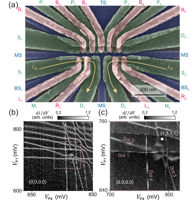
Four spin qubits are arranged in a linear array using an overlapping gate architecture, as shown in Fig. 1(a) Zajac et al. (2015). Single spin qubits are formed by accumulating a electron under each plunger gate: , , , and . The couplings between dots and between dots and the charge reservoirs formed beneath gates and are tuned by adjusting the barrier gate voltages . Charge sensing is performed by monitoring the currents and through two proximal quantum dot charge detectors located in the lower half of the device.
Charge stability diagrams for the array are shown in Figs. 1(b-c). To obtain good charge sensitivity for all four dot charge transitions = is plotted as a function of and . In Fig. 1(b) we show that we can achieve the charge state, where denotes the number of electrons in dot . The charge state is evident from the large region devoid of charge transitions in the lower left corner of the figure. The device is typically operated in the (1,1,1,1) charge state, which is labeled in the zoomed-in charge stability diagram of Fig. 1(c). The capacitive coupling between plunger gates and neighboring dots (i.e. gate P1 and dot 2) is naturally an order of magnitude weaker than the coupling between a plunger gate and the dot formed directly underneath it (i.e. gate P1 and dot 1) Zajac et al. (2015). It can therefore be challenging to distinguish charge transitions in adjacent dots (P1 and P2, or P3 and P4) in two-dimensional charge stability plots since the slopes are very similar. To more clearly distinguish the charge transitions, an artificial cross-coupling was added between each plunger gate and its neighboring plunger gates in software (details available in the supplementary information SOM ), such that a sweep of and induces transitions not only in dots 1 and 4, but also in dots 2 and 3. With the (1,1,1,1) charge state having been identified, we next establish virtual gates, which significantly streamline device tuning.
Virtual gates have been described in detail and compensate for the effects of device cross-capacitance through software corrections that effectively invert the capacitance matrix Mills et al. (2019); Baart et al. (2016); Hensgens et al. (2017); van Diepen et al. (2018); Volk et al. (2019). Whenever the voltage of gate is adjusted to tune the chemical potential of dot , the voltages on adjacent gates and are modified by a calibrated amount to keep the chemical potentials of dots and constant. The measured capacitance matrix is given in the supplementary information SOM and is used to establish the virtual gate space Mills et al. (2019).
Pairwise charge stability diagrams measured using virtual gates are shown in Figs. 2(a–c). As the two virtual gates and are swept, the charge sensor currents and are measured. Here we plot - as it results in higher charge sensing contrast. Gates not being swept [i.e. and in Fig. 2(a)] are held fixed at the same chemical potential as the source and drain reservoirs to enable fast loading and unloading of electrons throughout the array. The orthogonality of the charge transitions indicates that we have independent control of each quantum dot’s chemical potential.
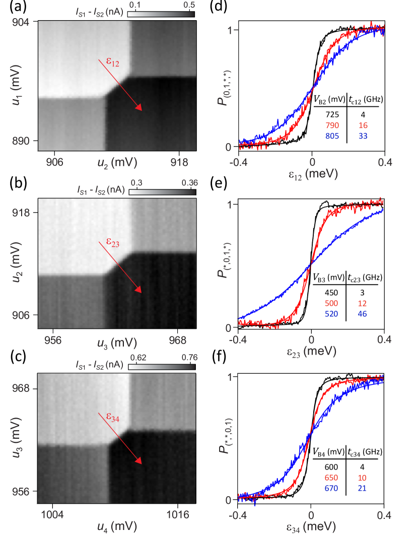
Loss & DiVincenzo suggested that the exchange interaction between two spins could be modulated by adjusting the height of the tunnel barrier separating the spins Loss and DiVincenzo (1998). We demonstrate control over all of the interdot tunnel couplings () in our device by measuring the charge state occupation as a function of detuning for different barrier gate voltages . Figure 2(d) plots along the detuning axis shown in Fig. 2(a). The * denotes that the chemical potential of the dot is held at the same value as the source and drain chemical potentials. As the tunnel coupling is increased, the charge delocalizes across adjacent dots and the interdot charge transition broadens. These data are fit as described in DiCarlo et al. (2004); Petta et al. (2004) to extract the interdot tunnel coupling. The lever arm conversion between gate voltage and energy is determined by measuring finite bias triangles for each pair of dots as reported in Table 1. As demonstrated by the data, the device offers a high degree of control, with tunnel coupling tunable from 2 GHz to many 10’s of GHz. Here is Boltzmann’s constant and the electron temperature 90 mK is determined by fitting the charge transitions to the source and drain to a Fermi function as described in Zajac et al. (2016).
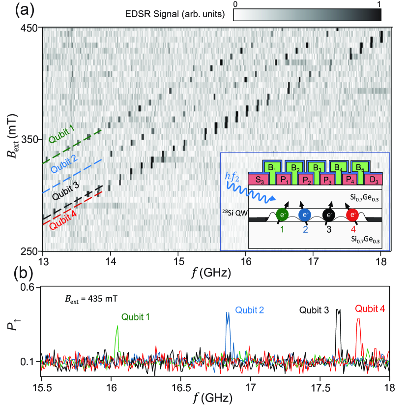
Site-selective single spin rotations are achieved using EDSR Pioro-Ladriere et al. (2008); Tokura et al. (2006) in the presence of a magnetic field gradient generated by a Co micromagnet SOM . The field from the micromagnet is different at each dot and therefore each spin has a unique electron spin resonance frequency given by , where is Planck’s constant, is the Landé g factor, and is the externally applied magnetic field. Our micromagnet design is similar to that used by Yoneda et al. Yoneda et al. (2015), but it has a slanting edge (as seen from above) that extends the field gradient over the entire quadruple quantum dot SOM .
To map out , EDSR spectroscopy is performed on each qubit. During spectroscopy, the array is configured such that only dot contains a single electron – all other dots are empty. A frequency chirped microwave pulse ( 15 MHz around a frequency for 120 s) is applied to gate MS. If the chirped pulse sweeps through the spin resonance frequency of dot , its spin will end up in a mixed state. Here our chirped pulses are not adiabatic, but are nonetheless convenient for identifying spin resonance conditions, as the linewidth of electron spins in 28Si can be narrow (100 kHz). The spin state of dot is then measured through spin-selective tunneling to the leads Elzerman et al. (2004). In the case of and , where the dots are not directly connected to the leads, the electron is shuttled to the edge of the array and read out in dots 1 or 4, respectively Mills et al. (2019). Loading the array follows the read out sequence in reverse. These measurements are repeated over a range of spanning 250 – 450 mT. The spectra for all four qubits are summed and plotted in Fig. 3(a). The field gradient from the micromagnet separates the qubit resonance frequencies by hundreds of MHz, as highlighted by the linecut through the data in Fig. 3(b). For comparison, in silicon devices relying on Stark shifts or interface disorder for spin selectivity, the qubit splitting is typically a few 10’s of MHz Veldhorst et al. (2015); Huang et al. (2018).
| Dot | (meV/mV) | E (meV) | (mT) | (s) | (s) |
|---|---|---|---|---|---|
| 1 | 0.14 | 4.5 | 137.6 | 2.6 | 41 |
| 2 | 0.13 | 4.7 | 165.8 | 1.5 | 31 |
| 3 | 0.14 | 4.5 | 194.3 | 10.4 | 72 |
| 4 | 0.15 | 4.7 | 199.2 | 9.4 | 109 |
We next measure the spin dephasing times and spin coherence times for each qubit (see Table 1). In natural silicon, spin coherence is limited by the hyperfine interaction with the 4.7% abundant 29Si nuclei. Here, our device consists of an isotopically enriched 28Si quantum well, which is 4.9 nm thick and has only an 800 ppm residual concentration of 29Si Deelman et al. (2016); Richardson et al. (2017). The buffer layers, however, consist of natSi and natGe containing residual spin-1/2 and spin-9/2 nuclei, respectively. Wavefunction overlap with these nuclei will be non-negligible given the relatively thin quantum well Witzel et al. (2012).
is determined through measurements of Ramsey fringes. For each Ramsey decay curve the data are integrated over 15 minutes. Qubits 3 and 4 show a nearly tenfold increase in compared with 1 s for electron spins in natural silicon, whereas qubits 1 and 2 have a dephasing time that is comparable to natural silicon. A simple Hahn echo pulse sequence significantly extends the coherence times, as summarized in Table. 1. Similar fluctuations in the coherence times have been observed in other devices Watson et al. (2018); Zajac et al. (2018); Huang et al. (2018) and may be due to sampling over a relatively small number of spin-carrying nuclei in the quantum well and SiGe barrier layers. Another reason for the fast dephasing in qubits 1 and 2 could be charge noise which has been shown to shorten Borjans et al. (2018) and Yoneda et al. (2018) in the presence of field gradients and is discussed in the supplementary information SOM . Due to the wedge shaped geometry of the micromagnet, the field gradient experienced by qubits 1 and 2 is significantly larger than at sites 3 and 4 which is evident from the large change in field offsets between dots 1-3, and a relatively small change in between dots 3 and 4 (see Table 1). The short coherence times in dots 1 and 2 are still comparable with the times reported in natural Si/SiGe and are not prohibitive for two-qubit operation.
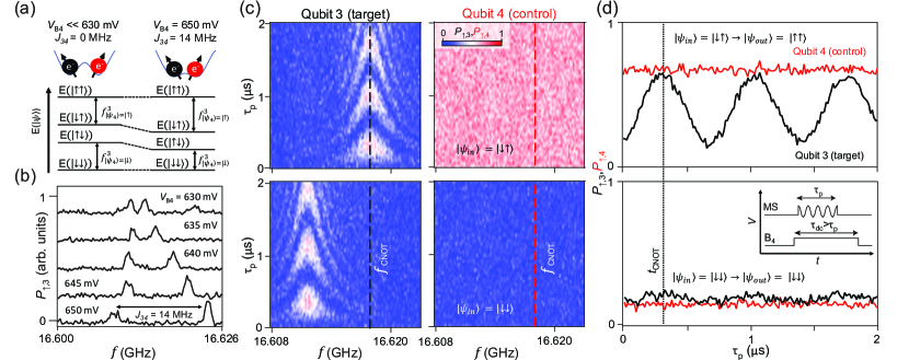
Two-qubit gates are performed by applying voltage pulses to the barrier gates separating the dots Loss and DiVincenzo (1998). Applying a positive voltage to a barrier gate increases wavefunction overlap between adjacent dots and turns on exchange Russ et al. (2018), as illustrated in the energy level diagram of Fig. 4(a). To first map out the influence of the barrier gate on the exchange interaction, we vary the gate voltage and perform EDSR spectroscopy on qubit 3, as shown in Fig. 4(b). Before measuring the EDSR spectrum of qubit 3, qubit 4 was prepared in a mixed state such that any state dependent line splitting could be observed Zajac et al. (2018). The EDSR spectrum of qubit 4 is probed in a similar way. As is increased, the EDSR lines split to reveal a doublet with a peak separation that is equal to the exchange energy . The overall frequency shift of the doublet is attributed to the displacement of the electron’s wavefunction within the magnetic field gradient as is adjusted Zajac et al. (2018).
A resonant-CNOT gate can be achieved using this device architecture by following the protocol developed by Zajac et al. Zajac et al. (2018). Here we focus on qubits 3 and 4. With , we prepare input state = through spin-selective tunneling or input state = through spin-selective tunneling followed by a -pulse on spin 4. We then apply a voltage pulse to gate to turn on exchange while simultaneously applying a microwave burst of varying duration and frequency . The resulting spin-up probabilities () for qubit 3(4) are plotted in Fig. 4(c). Rabi oscillations are observed for qubit 3 with a resonance frequency that is dependent on the state of qubit 4. By setting = , where the microwave tone is resonant with the target qubit when the control qubit is in the spin-up state, we drive Rabi oscillations on the target qubit conditioned on the state of the control qubit [see Fig. 4(d)]. Furthermore, when = , qubit 3 will be flipped when qubit 4 is in the spin-up state. With these settings, we realize a resonant-CNOT gate in a four qubit device Zajac et al. (2018); Russ et al. (2018). To implement a high fidelity CNOT gate, it is important to note that some additional phase accumulation due to the -induced Ising interaction must be compensated for by properly tuning and as described in our previous work Zajac et al. (2018); Russ et al. (2018). We attribute the slight oscillations that appear on qubit 3 in the lower panel of Fig. 4(d) to state preparation errors on qubit 4. Off-resonant driving would lead to oscillations at a frequency above 6 MHz.
In conclusion, we have demonstrated one- and two-qubit gate operations in a four qubit device fabricated from an isotopically enriched 28Si quantum well. Our device design allows for full control of the charge state in the array. Interdot tunnel coupling and exchange are tuned using barrier gates. We demonstrate independent control of all four qubits, which is enabled by the field gradient from a Co micromagnet. To demonstrate a two-qubit gate involving dots 3 and 4, we mapped exchange as a function of and performed a resonant-CNOT gate in 270 ns. These results set the stage for a four qubit spin-based quantum processor in silicon, which should be capable of performing small-scale quantum algorithms and demonstrating time crystal phases Barnes et al. (2019).
Funded by Army Research Office grant No. W911NF-15-1-0149, DARPA grant No. D18AC0025, and the Gordon and Betty Moore Foundation’s EPiQS Initiative through Grant GBMF4535. Devices were fabricated in the Princeton University Quantum Device Nanofabrication Laboratory.
References
- Loss and DiVincenzo (1998) D. Loss and D. P. DiVincenzo, “Quantum computation with quantum dots,” Phys. Rev. A 57, 120 (1998).
- Hanson et al. (2007) R. Hanson, L. P. Kouwenhoven, J. R. Petta, S. Tarucha, and L. M. K. Vandersypen, “Spins in few-electron quantum dots,” Rev. Mod. Phys. 79, 1217 (2007).
- Zwanenburg et al. (2013) F. A. Zwanenburg, A. S. Dzurak, A. Morello, M. Y. Simmons, L. C. L. Hollenberg, G. Klimeck, S. Rogge, S. N. Coppersmith, and M. A. Eriksson, “Silicon quantum electronics,” Rev. Mod. Phys. 85, 961 (2013).
- Tyryshkin et al. (2012) A. M. Tyryshkin, S. Tojo, J. J. L. Morton, H. Riemann, N. V. Abrosimov, P. Becker, H.-J. Pohl, T. Schenkel, M. L. W. Thewalt, K. M. Itoh, and S. A. Lyon, “Electron spin coherence exceeding seconds in high-purity silicon,” Nat. Mater. 11, 143 (2012).
- Veldhorst et al. (2014) M. Veldhorst, J. C. C. Hwang, C. H. Yang, A. W. Leenstra, B. De Ronde, J. P. Dehollain, J. T. Muhonen, F. E. Hudson, K. M. Itoh, A. Morello, and A. S. Dzurak, “An addressable quantum dot qubit with fault-tolerant control-fidelity,” Nat. Nanotechnol. 9, 981 (2014).
- Yoneda et al. (2018) J. Yoneda, K. Takeda, T. Otsuka, T. Nakajima, M. R. Delbecq, G. Allison, T. Honda, T. Kodera, S. Oda, Y. Hoshi, N. Usami, K. M. Itoh, and S. Tarucha, “A quantum-dot spin qubit with coherence limited by charge noise and fidelity higher than 99.9%,” Nat. Nanotechnol. 13, 102 (2018).
- Yang et al. (2018) C. H. Yang, K. W. Chan, R. Harper, W. Huang, T. Evans, J. C. C. Hwang, B. Hensen, A. Laucht, T. Tanttu, F. E. Hudson, S. T. Flammia, K. M. Itoh, A. Morello, S. D. Bartlett, and A. S. Dzurak, “Silicon qubit fidelities approaching incoherent noise limits via pulse optimisation,” arXiv:1807.09500 (2018).
- Veldhorst et al. (2015) M. Veldhorst, C. H. Yang, J. C. C. Hwang, W. Huang, J. P. Dehollain, J. T. Muhonen, S. Simmons, A. Laucht, F. E. Hudson, K. M. Itoh, A. Morello, and A. S. Dzurak, “A two-qubit logic gate in silicon,” Nature 526, 410 (2015).
- Zajac et al. (2018) D. M. Zajac, A. J. Sigillito, M. Russ, F. Borjans, J. M. Taylor, G. Burkard, and J. R. Petta, “Resonantly driven CNOT gate for electron spins,” Science 359, 439 (2018).
- Watson et al. (2018) T. F. Watson, S. G. J. Philips, E. Kawakami, D. R. Ward, P. Scarlino, M. Veldhorst, D. E. Savage, M. G. Lagally, M. Friesen, S. N. Coppersmith, M. A. Eriksson, and L. M. K. Vandersypen, “A programmable two-qubit quantum processor in silicon,” Nature 555, 633 (2018).
- Huang et al. (2018) W. Huang, C. H. Yang, K. W. Chan, T. Tanttu, B. Hensen, R. C. C. Leon, M. A. Fogarty, J. C. C. Hwang, F. E. Hudson, K. M. Itoh, A. Morello, A. Laucht, and A. S. Dzurak, “Fidelity benchmarks for two-qubit gates in silicon,” arXiv:1805.05027 (2018).
- Xue et al. (2018) X. Xue, T. F. Watson, J. Helsen, D. R. Ward, D. E. Savage, M. G. Lagally, S. N. Coppersmith, M. A. Eriksson, S. Wehner, and L. M. K. Vandersypen, “Benchmarking Gate Fidelities in a Si/SiGe Two-Qubit Device,” arXiv:1811.04002 (2018).
- Zajac et al. (2016) D. M. Zajac, T. M. Hazard, X. Mi, E. Nielsen, and J. R. Petta, “Scalable gate architecture for a one-dimensional array of semiconductor spin qubits,” Phys. Rev. Appl. 6, 054013 (2016).
- Noiri et al. (2016) A. Noiri, J. Yoneda, T. Nakajima, T. Otsuka, M. R. Delbecq, K. Takeda, S. Amaha, G. Allison, A. Ludwig, A. D. Wieck, and S. Tarucha, “Coherent electron-spin-resonance manipulation of three individual spins in a triple quantum dot,” Appl. Phys. Lett. 108, 153101 (2016).
- Otsuka et al. (2016) T. Otsuka, T. Nakajima, M. R. Delbecq, S. Amaha, J. Yoneda, K. Takeda, G. Allison, T. Ito, R. Sugawara, A. Noiri, A. Ludwig, A. D. Wieck, and S. Tarucha, “Single-electron spin resonance in a quadruple quantum dot,” Sci. Rep. 6, 31820 (2016).
- Ito et al. (2018) T. Ito, T. Otsuka, T. Nakajima, M. R. Delbecq, S. Amaha, J. Yoneda, K. Takeda, A. Noiri, G. Allison, A. Ludwig, A. D. Wieck, and S. Tarucha, “Four single-spin Rabi oscillations in a quadruple quantum dot,” Appl. Phys. Lett. 113, 093102 (2018).
- Mortemousque et al. (2018) P.-A. Mortemousque, E. Chanrion, B. Jadot, H. Flentje, A. Ludwig, A. D. Wieck, M. Urdampilleta, C. Bauerle, and T. Meunier, “Coherent control of individual electron spins in a two dimensional array of quantum dots,” arXiv:1808.06180 (2018).
- Mukhopadhyay et al. (2018) U. Mukhopadhyay, J. P. Dehollain, C. Reichl, W. Wegscheider, and L. M. K. Vandersypen, “A 2x 2 quantum dot array with controllable inter-dot tunnel couplings,” Appl. Phys. Lett. 112, 183505 (2018).
- Reed et al. (2012) M. D. Reed, L. DiCarlo, S. E. Nigg, L. Sun, L. Frunzio, S. M. Girvin, and R. J. Schoelkopf, “Realization of three-qubit quantum error correction with superconducting circuits,” Nature 482, 382 (2012).
- Schindler et al. (2011) P. Schindler, J. T. Barreiro, T. Monz, V. Nebendahl, D. Nigg, M. Chwalla, M. Hennrich, and R. Blatt, “Experimental repetitive quantum error correction,” Science 332, 1059 (2011).
- Hensgens et al. (2017) T. Hensgens, T. Fujita, L. Janssen, X. Li, C. J. van Diepen, C. Reichl, W. Wegscheider, S. Das Sarma, and L. M. K. Vandersypen, “Quantum simulation of a Fermi-Hubbard model using a semiconductor quantum dot array,” Nature 548, 70 (2017).
- Georgescu et al. (2014) I. M. Georgescu, S. Ashhab, and F. Nori, “Quantum simulation,” Rev. Mod. Phys. 86, 153 (2014).
- Barthelemy and Vandersypen (2013) P. Barthelemy and L. M. K. Vandersypen, “Quantum dot systems: a versatile platform for quantum simulations,” Ann. Phys. 525, 808 (2013).
- Byrnes et al. (2008) T. Byrnes, N. Y. Kim, K. Kusudo, and Y. Yamamoto, “Quantum simulation of fermi-hubbard models in semiconductor quantum-dot arrays,” Phys. Rev. B 78, 075320 (2008).
- Barnes et al. (2019) E. Barnes, J. M. Nichol, and S. E. Economou, “Stabilization and manipulation of multispin states in quantum-dot time crystals with heisenberg interactions,” Phys. Rev. B 99, 035311 (2019).
- Petta et al. (2005) J. R. Petta, A. C. Johnson, J. M. Taylor, E. A. Laird, A. Yacoby, M. D. Lukin, C. M. Marcus, M. P. Hanson, and A. C. Gossard, “Coherent manipulation of coupled electron spins in semiconductor quantum dots,” Science 309, 2180–2184 (2005).
- Russ et al. (2018) M. Russ, D. M. Zajac, A. J. Sigillito, F. Borjans, J. M. Taylor, J. R. Petta, and G. Burkard, “High-fidelity quantum gates in Si/SiGe double quantum dots,” Phys. Rev. B 97, 085421 (2018).
- Zajac et al. (2015) D. M. Zajac, T. M. Hazard, X. Mi, K. Wang, and J. R. Petta, “A reconfigurable gate architecture for Si/SiGe quantum dots,” Appl. Phys. Lett. 106, 223507 (2015).
- (29) See Supplemental Material at [URL will be inserted by publisher] for additional device characterization data including references Mills et al. (2019); Yoneda et al. (2015); Zajac et al. (2016); Klauder and Anderson (1962); Witzel et al. (2010); Yoneda et al. (2018); Borjans et al. (2018).
- Mills et al. (2019) A. R. Mills, D. M. Zajac, M. J. Gullans, F. J. Schupp, T. M. Hazard, and J. R. Petta, “Shuttling a single charge across a one-dimensional array of silicon quantum dots,” Nat. Commun. 10, 1063 (2019).
- Baart et al. (2016) T. A. Baart, M. Shafiei, T. Fujita, C. Reichl, W. Wegscheider, and L. M. K. Vandersypen, “Single-spin CCD,” Nat. Nanotechnol. 11, 330 (2016).
- van Diepen et al. (2018) C. J. van Diepen, P. T. Eendebak, B. T. Buijtendorp, U. Mukhopadhyay, T. Fujita, C. Reichl, W. Wegscheider, and L. M. K. Vandersypen, “Automated tuning of inter-dot tunnel coupling in double quantum dots,” Appl. Phys. Lett. 113, 033101 (2018).
- Volk et al. (2019) C. Volk, A. M. J. Zwerver, U. Mukhopadhyay, P. T. Eendebak, C. J. van Diepen, J. P. Dehollain, T. Hensgens, T. Fujita, C. Reichl, W. Wegscheider, and L. M. K. Vandersypen, “Loading a quantum-dot based “Qubyte” register,” arXiv:1901.00426 (2019).
- DiCarlo et al. (2004) L. DiCarlo, H. J. Lynch, A. C. Johnson, L. I. Childress, K. Crockett, C. M. Marcus, M. P. Hanson, and A. C. Gossard, “Differential charge sensing and charge delocalization in a tunable double quantum dot,” Phys. Rev. Lett. 92, 226801 (2004).
- Petta et al. (2004) J. R. Petta, A. C. Johnson, C. M. Marcus, M. P. Hanson, and A. C. Gossard, “Manipulation of a single charge in a double quantum dot,” Phys. Rev. Lett. 93, 186802 (2004).
- Pioro-Ladriere et al. (2008) M. Pioro-Ladriere, T. Obata, Y. Tokura, Y.-S. Shin, T. Kubo, K. Yoshida, T. Taniyama, and S. Tarucha, “Electrically driven single-electron spin resonance in a slanting Zeeman field,” Nat. Phys. 4, 776 (2008).
- Tokura et al. (2006) Y. Tokura, W. G. van der Wiel, T. Obata, and S. Tarucha, “Coherent single electron spin control in a slanting Zeeman field,” Phys. Rev. Lett. 96, 047202 (2006).
- Yoneda et al. (2015) J. Yoneda, T. Otsuka, T. Takakura, M. Pioro- Ladrière, R. Brunner, H. Lu, T. Nakajima, T. Obata, A. Noiri, C. J. Palmstrøm, A. C. Gossard, and S. Tarucha, “Robust micromagnet design for fast electrical manipulations of single spins in quantum dots,” APEX 8, 084401 (2015).
- Elzerman et al. (2004) J. M. Elzerman, R. Hanson, L. H. W. Van Beveren, B. Witkamp, L. M. K. Vandersypen, and L. P. Kouwenhoven, “Single-shot read-out of an individual electron spin in a quantum dot,” Nature 430, 431 (2004).
- Deelman et al. (2016) P. W. Deelman, L. F. Edge, and C. A. Jackson, “Metamorphic materials for quantum computing,” Mater. Res. Bull. 41, 224 (2016).
- Richardson et al. (2017) C. J. K. Richardson, C. A. Jackson, L. F. Edge, and P. W. Deelman, “High-resolution x-ray reflection Fourier analysis of metamorphic Si/SiGe quantum wells,” J. Vac. Sci. Technol. B 35, 02B113 (2017).
- Witzel et al. (2012) W. M. Witzel, M. S. Carroll, L. Cywiński, and S. Das Sarma, “Quantum decoherence of the central spin in a sparse system of dipolar coupled spins,” Phys. Rev. B 86, 035452 (2012).
- Borjans et al. (2018) F. Borjans, D. M. Zajac, T. M. Hazard, and J. R. Petta, “Single-spin relaxation in a synthetic spin-orbit field,” arXiv:1811.00848 (2018).
- Klauder and Anderson (1962) J. R. Klauder and P. W. Anderson, “Spectral diffusion decay in spin resonance experiments,” Phys. Rev. 125, 912–932 (1962).
- Witzel et al. (2010) W. M. Witzel, M. S. Carroll, A. Morello, L. Cywiński, and S. Das Sarma, “Electron spin decoherence in isotope-enriched silicon,” Phys. Rev. Lett. 105, 187602 (2010).