Theoretical Prediction of Stable Cluster-assembled CdSe Bilayer and its Functionalization with Co and Cr Adatoms
Abstract
In this article, we present our results on bilayers assembled upon strategic placement of Cd6Se6 clusters. These bilayers are studied for their stability and electronic structure with the help of density functional theory and are further analyzed using Bardeen, Tersoff and Hamann formalism for their tunneling properties. Our calculations show that the hexagonal arrangement of these clusters prevails as the most stable geometry showing all real phonon modes. First-principles molecular dynamics studies on this 2D structure show that it remains intact even at room temperature. This bilayer shows an indirect semiconducting band gap of 1.28 eV with the current-voltage (I-V) characteristics similar to a tunnel diode. Further, we functionalized this bilayer using transition metal atoms, Co and Cr. The aim was to seek whether the bilayer sustains magnetism and how the concentration affects its electronic and magnetic properties. Co functionalization brings ferromagnetic ordering in the bilayer which turns near half-metallic upon increasing the concentration. On the other hand, Cr functionalization shows a transition from antiferro- to ferromagnetic ordering upon increasing the concentration. The I-V characteristics of all these functionalized bilayers show negative differential conductance similar to a tunnel diode.
pacs:
I Introduction
Cluster-assembled materials, in which atomic clusters are arranged methodically in a periodic array to form a solid, are emerging materials for their technological applications. Also known as nanostructured materials, they allow the integration of multiple length scales into a hierarchical material Claridge et al. (2009). With precisely controlled building-blocks, such synergistic cluster-assemblies can be used to create multitudes of periodic structures having unusual symmetries that are “custom-made” for specific requirements. Although various successful attempts have been made to explore the possibility of existence of such materials Claridge et al. (2009), smaller sized clusters are difficult to handle experimentally. Thus, modeling these materials theoretically, generates an impetus for experimental processes.
Modern era of materials research revolves around 2-dimensional (2D) materials as a consequence of discovery of graphene Geim and Novoselov (2007); Allen et al. (2010). Recent times have witnessed an emergence of variety of different 2D materials that have not only opened new avenues of fundamental research but also of device designs. Amidst the deluge of 2D materials, pseudo-planar and van der Waals (vdW) bonded layered materials have maintained their own identity Molle et al. (2017); Jariwala et al. (2017). Keeping with the current research trends, we planned to explore the cluster-assembled vdW bonded bilayers of CdSe consisting of buckled pseudo-planar sheets. Also, having predicted the existence of such bilayer theoretically, we further wanted to see whether the bilayer can form ordered spin structures, upon introduction of transition metal (TM) atoms. We speculate that such materials can facilitate a number of potential functionalities that can be readily engineered. Earlier such attempts were made by Liu et al. in their studies of cluster-assembled sheets of endohedrally doped Si12 clusters with vanadium atoms Liu et al. (2015). They observed that two different types of cluster-assembled sheets prefer ferromagnetic ordering with free-electron-mediated mechanism.
This article presents our results on bilayers assembled using Cd6Se6 clusters that we further functionalize with the help of TM atoms, Co and Cr. We also simulate scanning tunneling spectroscopy results by calculating the tunneling properties of these pristine and functionalized bilayers with the help of Bardeen, Tersoff and Hamann (BTH) formalism Bardeen (1961); Tersoff and Hamann (1983) combined with first-principles density functional theory (DFT) approach.
II Computational details
Our calculations for Cd6Se6 cluster-assembled bilayers are based on DFT formalism as implemented in Vienna Ab-initio Simulations Package (VASP) Kresse and Furthmüller (1996). The structural and electronic properties are obtained with the help of exchange-correlation energy functional as given by Perdew, Burke and Ernzerhof (PBE) with projector-augmented-wave (PAW) method used to describe the core electrons Perdew et al. (1996); Blöchl (1994). The self-consistent convergence criterion of energy is set to 10-5 eV. The occupation numbers are treated according to the Gaussian scheme with a broadening of 0.001 eV. The bilayers are constructed (in the xy-plane) in such a manner that the two periodic images are separated by a distance of 15 Å (in the z-direction). In order to optimize the structures, relaxation procedures are carried out according to conjugate gradient algorithm. The relaxation is achieved with the help of Hellmann-Feynman forces and the stress tensors by taking appropriate derivatives of total energy of the unit cell in every iteration with the convergence threshold on forces set as 0.01 eV/Å. The Brillouin zone (BZ) is represented by the Monkhorst-Pack k-point mesh of . For weak interactions involved in the computation, due to the presence of bilayered structures, we have used PBE+D3 method with Grimme vdW corrections as implemented in VASP Grimme et al. (2010). To understand the structural stability, phonon bandstructure and density of states (DOS) are calculated using density functional perturbation theory with the help of linear response method Togo and Tanaka (2015).
In order to study the tunneling properties of these pristine and functionalized bilayers, we use BTH formalism as implemented by He et al. He et al. (2006) in their scanning tunneling microsope (STM)-like setup. As per this formalism, the electron tunneling current can be calculated in the low-bias limit using first-order perturbation theory as follows:
where and are the projected densities of states (PDOS) of the sample and the tip respectively, is the tip to sample distance, is the injection energy of the tunneling electron, is the electronic charge, is the effective mass of the electron, is the Planck constant, is the average work-function of the sample and the tip and is the Fermi distribution function. In this particular formalism, due to the low-bias criterion and are assumed to be constant. Since, the tip and the sample are assumed to be in electrochemical equilibrium, their Fermi energies are aligned and are taken to be the reference energy in the above equation. Bias-induced changes are not included on the sample DOS, which occur only at high applied bias. In our STM-like setup, the sample is the bilayer (pristine/functionalized), while the tip is modeled by 7-atom gold cluster. This fully relaxed tip geometry is chosen to mimic the sharp STM tip. The DOS of the STM-tip is artificially broadened (broadening factor 0.2 eV) to consider the broadening due to the semi-infinite nature of the tip. While designating the value of broadening, the reported value for life time broadening of electrons in a cluster in a scanning tunneling spectroscopy study is taken into account Bolotov et al. (2001).
III Results and discussion
III.1 Geometry and electronic structure of CdSe bilayers
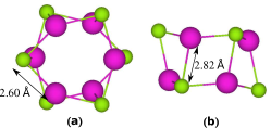
Motivation behind this study is to examine whether an assembly of small CdSe clusters can form stable 2D-sheets that can further be used in different applications. As a first step towards this, we chose Cd6Se6 cluster which is the smallest wurtzite cage with symmetry as observed by Jose et al. Jose et al. (2006). The cluster consists of two planar Cd3Se3 clusters stacked on top of each other in chair conformation, where each Cd3Se3 cluster forms a hexagon of side 2.60 Å and the Cd-Se stacking distance is 2.82 Å (see Figure 1).
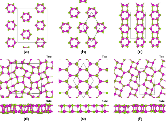
There may be a large number of possible 2D configurations to be found by arranging Cd6Se6 clusters as building blocks. Here we design three configurations and let them undergo unconstrained relaxation. These configurations are shown in the upper panel of Figure 2 (a), (b) and (c), and are named as Type-1, Type-2 and Type-3 structures. The corresponding geometries of these configurations upon relaxation are shown in Figure 2 (d), (e) and (f). In each of these cases, the clusters form bilayered sheets that show buckling in both the layers. Out of these three structures, Type-2 has the smallest number of atoms in the unit cell (6 Cd and 6 Se atoms) with a hexagonal lattice (7.83 Å) i.e. the unit cell consists of a single Cd6Se6 unit. Unit cell of Type-1 bilayer consists of four units of Cd6Se6 cluster (lattice parameters, and ) and that of Type-3 bilayer consists of two units of Cd6Se6 cluster (lattice parameters, and ). Average width of the bilayer in Type-1 (2.78 Å) mostly remains uniform with the most uneven distribution of in-plane Cd-Se bond lengths ranging from 2.65 Å to 2.78 Å, amongst the three bilayers. For Type-2 structure, the bilayer width varies between 2.82 Å and 2.91 Å. The average Cd-Se bond length in this case is 2.64 Å and the hexagons formed by Cd-Se atoms are not regular. Average width of the bilayer in Type-3 geometry is 2.82 Å with in-plane Cd-Se bond lengths varying from 2.62 Å to 2.78 Å. Comparing all the relaxed geometries we observe that Type-2 structure has the highest symmetry amongst the three types and it shows similar structure to that of type stacking in -BN bilayers Constantinescu et al. (2013). is shown to be the most stable stacking order in -BN bulk and bilayer forms, both experimentally as well as theoretically. Type-1 structure shows a bilayer composed of hexagons and quadrilaterals, whereas optimized geometry of Type-3 structure contains a stretched array formed of octagons and hexagons.
The relaxed geometries were further compared energetically to understand their relative stabilities. We calculated the binding energy () per atom as follows,
| (1) |
| Structure | |
|---|---|
| (eV) | |
| Type-1 | -2.67 |
| Type-2 | -2.79 |
| Type-3 | -2.69 |
The values of are shown in Table 1 for all the three
structures and they differ only marginally. It can be seen that Type-2
structure, which has the highest symmetry also has the lowest value.
This indeed reiterates that layered materials are predominantly formed in
hexagonal symmetries, including different stacking orders of the hexagonal
layers Constantinescu et al. (2013). To confirm the stability of Type-2 assembly (owing to its
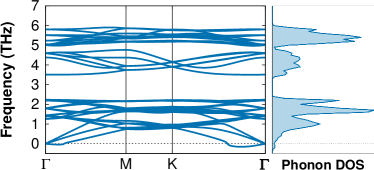
lowest value), we calculated its phonon bandstructures that is shown in
Figure 3. With the exception of small imaginary frequencies around
the point of the BZ the phonon bandstructure does not show any
unstable phonon modes confirming its stability. Small imaginary frequencies
(<10 THz) can be attributed to the limitations of the numerics.
Further, it is imperative to study whether the predicted 2D
material withstands small temperature fluctuations. Hence, we performed
molecular dynamics (MD) simulations at room temperature i.e. 300K
for 10000 fs. We observed that apart from some small thermal
fluctuations the Type-2 structure remains in tact. Thus, our observed lowest
energy cluster-assembled 2D bilayer of CdSe, is thermally stable upto 300K.
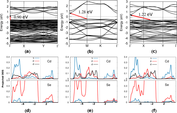
Figure 4 shows the electronic bandstructures and PDOS of Cd6Se6 cluster-assembled bilayers. Type-1 structure has a direct band gap of 0.90 eV at point of the BZ, whereas Type-2 structures has an indirect band gap of 1.28 eV from . Type-3 structure also shows an indirect band gap of 1.23 eV where the conduction band minimum (CBM) lies between and points and the valence band maximum (VBM) lies at the point of the BZ. In all the three structures, the VBM consists of Se and Cd states with Se being predominant and the CBM is made up of Cd states. CdSe, in its bulk form has been reported to have experimental band gap of 1.84 eV at 0 K Kittel (1986), whereas our calculations for bulk wurtzite form of CdSe show a band gap of 0.53 eV. This happens due to the tendency of DFT to underestimate the band gaps and we expect that just as the case of bulk CdSe, the actual band gaps for our bilayers, would even be higher than our reported values. Hence, the cluster-assembled bilayers, studied in the current work, may show band gaps larger than that of bulk CdSe.
III.2 Transition metal doped CdSe bilayers
We now present the effects of TM adatoms in our Type-2 CdSe bilayer that we obtained as the most stable cluster-assembled sheet. TM doping in a semiconductor is a viable way to improve its properties as a probable material for spintronic device. Group II-VI semiconductors doped with different TM atoms have been investigated as diluted magnetic semiconductors by various researchers. Co doping is known to induce antiferromagnetic behaviour in bulk CdSe Niu et al. (1990) whereas Cr doping in II-VI semiconductors shows ferromagnetic behaviour Niwayama et al. (2008); Shrivastava et al. (2011). For our study, we investigated their effects on structural, magnetic and electronic properties of the bilayer. There are two fundamentally different locations for the introduction of adatoms: one in-between the layers and other on the top. Our calculations indicate that upon insertion of TM adatom in between the layers, our structure gets highly distorted resulting in non-Cd6Se6 configuration. Therefore we report only the later case hereafter. We present two cases of Co/Cr adsorbed on top of Type-2 Cd6Se6 cluster-assembled bilayer. In the first one, single TM atom is kept on top of center of every hexagon giving 50% adsorption per Cd-Se pair in the bilayer, while in the second case a single TM atom is kept on top of center of alternate hexagon giving 17% adsorption per bilayer atom. With these initial geometries we performed unconstrained relaxation to obtain the minimum energy solution. Additionally, magnetic ground state is determined by unconstrained minimization of all possible magnetic configurations. Below we report only the ground state magnetic configuration of 50% and 17% concentration of Co and Cr adatoms over Type-2 CdSe bilayer.
III.2.1 Structural, electronic and magnetic properties : Co-adatom
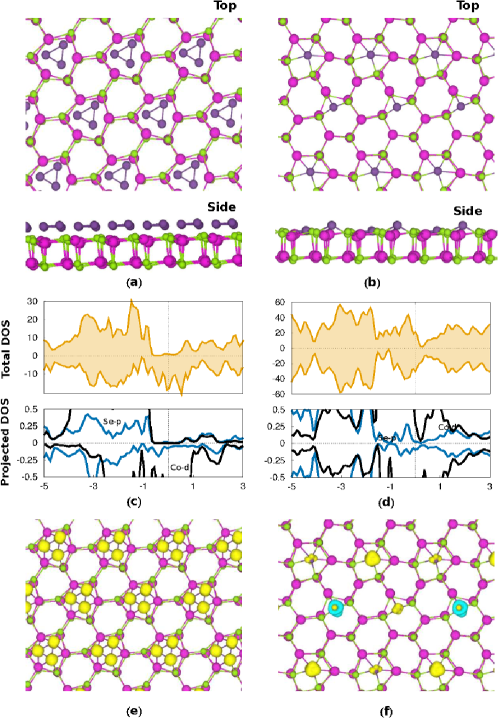
We notice that for higher concentration of Co-adatom (50%), a tendency of clustering of Co atoms is seen over the bilayer (see Figure 5 (a)). Crossing over the underlying bonds Co atoms form triangular geometries over every alternate hexagon along the armchair direction. The distorted triangle has a mean bond length of 2.23 Å, and is located at a distance of 2.11 Å above the bilayer. The underlying bilayer also distorts to accommodate the adatoms. The resulting system is ferromagnetic with a magnetic moment of 10.19 /unit cell and has a per atom of -3.73 eV. This behaviour is also seen from the total DOS and PDOS in Figure 5 (c). Spin-up DOS for this configuration shows a gap near Fermi energy, whereas the spin-down DOS shows conducting nature resulting in half-metalic behaviour. Spin-down channel mainly conducts through Co states, that are empty in spin-up channel. Se states also acquire small magnetization due to the presence of Co atoms. This bahaviour is different than bulk where Co impurities are antiferromagnetically coupled. Antiferromagnetic state of the same configuration lies 0.58 eV above the ferromagnetic state.
Upon reducing the concentration of Co to 17%, as seen from Figure 5 (b), similar to the previous case, the adatoms move away from their initial positions and the underlying bilayer distorts. Similar to its 50% counterpart, the TM atoms are ferromagnetically coupled and the system has a of -2.87 eV/atom. The magnetic moment now reduces to 1.00 /unit cell. Co atoms have an average distance of 7.42 Å between each other. The ferromagnetic nature is also seen from the total and site projected DOS plots shown in Figure 5 (d). We can see the presence of gap states near Fermi energy in both spin-up and spin-down channels that originate mainly due to the presence of Co states. Thus, one can see the possibility to tune the band gap and magnetism using concentration of Co. Moreover one can also speculate that certain concentration (50%) of Co-adatom may give rise to half-metallic phases - a feature that has been rarely investigated in 2D materials.
III.2.2 Structural, electronic and magnetic properties : Cr-adatom
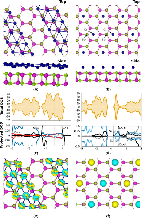
Cr-adsorption at 50% concentration, upon full relaxation, also shows
clustering tendency, but unlike Co where atoms form islands, here atoms form
ribbons. As seen in Figure 6 (a), Cr adatoms form ribbons of width
5.07 Å along the armchair direction resulting in an array of triangular
structures. The mean bond length in the triangle is 3.60 Å and two stripes
are separated by 9.45 Å. Unlike Co-adsorption, small degree of distortion
is observed in the underlying CdSe bilayer. Triangular array obviously opens up
the possibility of several magnetic structures. We performed series of
calculations of ferromagnetic and antiferromagnetic ordering and found that the
ferromagnetic and antiferromagnetic states are barely separated in energy by
only 1 meV/atom with the value of as -3.41 eV. The magnetic moment
in case of ferromagnetic phase is 1.00/unit cell. In Figure 6
(c), we present the total DOS and PDOS of the ferromagentic phase, which mainly
originates from Cr states with Cd and Se states showing their
presence by acquiring small magnetization.
On the other hand, lower concentration of Cr (17%) prefers to be in
antiferromagnetic phase. As seen from Figure 6 (b), the geometry of
the bilayer does not change much and despite being 7.84 Å apart, Cr
atoms are coupled antiferromagnetically (See Figure 6 (d)). In the
figures of total DOS and PDOS (See Figure 6 (d)), the antiferromagnetic
coupling is indicated by showing states of two Cr atoms with black and
grey; and states of two Se atoms with blue and light blue. As discussed
before, for both the concentrations of Cr, the effective magnetic moment is
fairly small. This is also evident from the spin density plots of these
structures shown in Figure 6 (e) and (f). It is worth noticing that for
higher concentration, the magnetic order is destroyed. This behaviour is
opposite to the behaviour of bulk Cr-doped CdSe system. Thus we expect that
with further increase in concentration, system will become non-magnetic. Thus
of Cr offers a viable way to achieve desired magnetic phases.
The most noticeable difference between the two adatoms is that changing the concentration of Co adatoms can tune the band gap and can help get desirable magnetic moment whereas changes in the Cr concentration changes the magnetic nature of the bilayer. Co adatom has strong binding which also results in clustering of the adatoms and structural deformation of bilayer. Cr adatoms, on the other hand forms highly ordered patterns, maintaining the structure of the underlying bilayer.
III.2.3 Tunneling properties
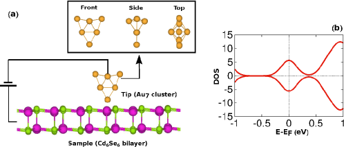
We now investigate the pristine and TM doped bilayers with the help of BTH formalism. BTH formalism is well-suited in the limits of small bias voltage (V), , where is the work function of the tip. Considering the typical metal work function, = 4 eV, bias voltage range below 2 V can typically be useful in BTH formalism Sattler (2010). In our current work, the STM-like setup consists of pristine/functionalized Type-2 Cd6Se6 bilayer as sample and 7-atom gold cluster as tip (see Figure 7 (a)). This fully relaxed tip geometry is chosen to mimic the sharp STM tip. The DOS of the STM-tip is artificially broadened (broadening factor 0.2 eV) to consider the broadening due to the semi-infinite nature of the tip. It should be noted that the Au7 cluster that we are incorporating as a tip has paramagnetic ground state that is also evident in the DOS of the tip in Figure 7 (b).
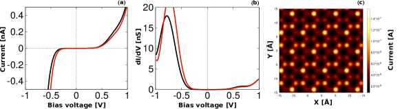
In Figure 8 we present the calculated tunneling characteristics of Type-2 Cd6Se6 bilayer for a low-bias range of -1.0 V to 1.0 V. The I-V characteristics are computed at Cd and Se sites on the bilayer. By positioning the tip exactly above these sites, we obtain the spatially resolved tunneling spectra. These spectra are directly dependent on the sum of the relevant site projected DOS of atoms in that plane and the adjoining planes till the exponential distance factor in the tunneling current equation becomes negligible. I-V characteristics for the bilayer are shown in Figure 8 (a). The curves are obtained upon sweeping the tip bias and calculating the current at a particular lateral tip position, keeping the tip to sample distance fixed (4.5Å). The I-V characteristics show rectification nature since no states are available in the gap region (1.28 eV) to contribute to the tunneling current. Figure 8 (b) shows the differential conductance (dI/dV) characteristics which correlates well with the LDOS of the structure calculated using DFT. Changing the tip-sample separation affects the magnitude of tunneling current, but the nature of graphs remains unaffected. We also simulate the constant height mode STM images for the bilayer as shown in Figure 8 (c). These images provide the topography of this quasi-2D structure. The height above the bilayer at which the constant height mode image is taken, is chosen such that the optimum resolution of the bilayer is obtained. The geometric features of the bilayer are clearly seen in this image indicating the hexagonal patterns in the form of bright spots (i.e. Cd and Se atoms). The brightness of the atoms shows their relative proximity to the tip.
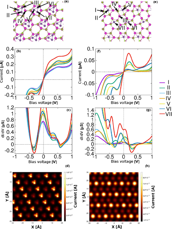
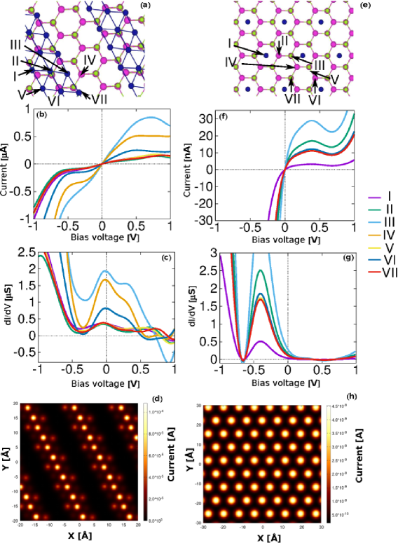
We now focus our attention on the tunneling properties of the TM doped bilayer for different compositions. The results for these are compiled in Figures 9 and 10 for Co doped and Cr doped bilayers respectively. In these figures, the tip positions are numbered and colour coded. Graph for each position is then drawn with the same colour in all the further figures depicting I-V characteristics corresponding to various positions numbered as I to VII in Figures (b) and (f), dI/dV curves in Figures (c) and (g) and constant height mode images in (d) and (h).
Let us first discuss the results for Co adsorbed bilayer presented in Figure 9. The I-V curves for all the positions for higher (Figure 9 (b)) as well as lower concentration (Figure 9 (f)) maintain the linearity near zero bias, which is consistent with their overlapping valence and conduction states seen in the DOS. It is known that the tunneling current is directly related to the convolution of relevant regions of the local density of states (LDOS) of tip and sample. Since there is finite LDOS at Fermi energy we see increase in tunneling current with increase in applied bias voltage. This behaviour is consistently present at every position of 50% Co-doped bilayer, but as the bias voltage reaches 0.5 V, we observe that the tunneling current starts decreasing with an increase in the bias voltage. The tunneling current decays upto a certain bias voltage range and begins to rise again as bias increases further. This feature is known as negative differential conductance (NDC) and it is characteristic of tunnel diode. NDC is seen in the dI/dV characteristics which correlates well with the LDOS calculated using DFT (see Figure 9 (c)). In case of 17% Co-doped bilayer, the NDC arises at tip bias of 0.20 V and it is much more pronounced than that in case of 50% Co-adsorption. dI/dV characteristics of 17% Co-doped bilayer are seen in Figure 9 (g). For both the concentrations, the NDC features are also seen in negative bias region. NDC indicates that no states are available for tunneling in the energy range resulting in a little overlap of LDOS of Au-tip and the Co-doped bilayer, therefore there is decrease in the tunneling current even with an increase in bias voltage. The onset of NDC results from a sharp drop in the tunneling probability when bias voltage reaches an energy level at which tunneling is forbidden. For higher composition of Co-dopant (50%), the higher density of TM states allows the current to increase more-or-less in linear fashion. Reduction in the Co-dopant concentration reduces the number of energy levels allowed for transition, hence reducing the tunneling current and giving rise to more pronounced NDC features. Constant height mode STM images are also depicted in Figure 9 (d) and (h). These images reveal the geometric features of the Co-doped bilayers. In Figure 9 (d), one can notice the triangular patterns formed by Co atoms on top of the bilayer. But only the atoms in the alternate rows of triangles are resolved well due to the fact that the alternate triangles are placed slightly ( 0.2 Å) closer to the bilayer than others. In Figure 9 (h), Cd and Se atoms in the same plane as that of Co are also observed as bright spots.
Figure 10 shows the tunneling characteristics of the bilayer with Cr adsorption. Similar to the Co-adsorption, one can observe the NDC features in Cr-doped bilayer for both the concentrations. The NDC exists in the region of bias voltage where there is minimum in the tip DOS. This is also confirmed in dI/dV plots for both the concentrations (see Figures 10 (c) and (g)). Constant height mode STM images for Cr-doped bilayers are shown in Figure 10 (d) and (h). In Figure 10 (d), the ribbon-like patterns made by Cr atoms are clearly seen. The atoms that look diffused in these ribbons are the ones that are not in the same plane. Similarly, in Figure 10 (h), one can see the Cr-atoms in the form of hexagonal patterns.
IV Conclusions
To summarize, we predicted and analyzed novel quasi-2D structures of CdSe built intuitively using clusters as building blocks. We also functionalized them to demonstrate their ability to control their electronic and magnetic properties. The most stable configuration of CdSe bilayer shows an indirect band gap of 1.28 eV and I-V characteristics of a schottky diode. The bilayer shows dynamical stability via all real phonon modes and sustains the temperatures upto 300K as evident from our MD calculations.
We used TM atoms, Co and Cr, to functionalize the most stable configuration of the bilayer. We found that even small concentration of Co adatoms, reorganizes the bilayer to make it ferromagnetic. Upon increasing the Co concentration, system shows tell-tale signs of half-metallic systems. It remains to be seen if pure half-metallic behaviour can be obtained for certain concentration. On the other hand, Cr doping shows a transition from ferro to antiferromagnetic ordering upon decreasing the adatom concentration. The exciting effect of doping is seen in the I-V characteristics, which we compute using BTH formalism. While pristine bilayer shows classic Schottky diode-like features, we found that the functionalized system shows the characteristics of a tunnel diode via NDC.
We expect that our studies bring out the versatile nature of the cluster-assembled CdSe bilayer that can find novel applications in the field of electronics and spintronics.
AK acknowledges the financial support from the Nanomission Council, Department of Science & Technology, Government of India (Grant code: SR/NM/NS-15/2011(G)) through a major research project and DST-PURSE and DST-FIST grants to Savitribai Phule Pune University and Department of Physics, respectively. DS acknowledges financial support from Universities Grant Commission - Basic Scientific Research (UGC-BSR) through a fellowship. We also thank C-DAC, Pune for use of their computing facilities. The geometries of all the structures shown in this article are generated using VESTA Momma and Izumi (2008).
References
- Claridge et al. (2009) S. A. Claridge, A. W. Castleman Jr., S. N. Khanna, C. B. Murray, A. Sen, and P. S. Weiss, ACS Nano 3, 244 (2009).
- Geim and Novoselov (2007) A. K. Geim and K. S. Novoselov, Nat. Mater. 6, 183 (2007).
- Allen et al. (2010) M. J. Allen, V. C. Tung, and R. B. Kaner, Chem. Rev. 110, 132 (2010).
- Molle et al. (2017) A. Molle, J. Goldberger, M. Houssa, Y. Xu, S.-C. Zhang, and D. Akinwande, Nat. Mater. 16, 163 (2017).
- Jariwala et al. (2017) D. Jariwala, T. J. Marks, and M. C. Hersam, Nat. Mater. 16, 170 (2017).
- Liu et al. (2015) Z. Liu, X. Wang, J. Cai, and H. Zhu, J. Phys. Chem. C 119, 1517 (2015).
- Bardeen (1961) J. Bardeen, Phys. Rev. Lett. 6, 57 (1961).
- Tersoff and Hamann (1983) J. Tersoff and D. R. Hamann, Phys. Rev. Lett. 50, 1998 (1983).
- Kresse and Furthmüller (1996) G. Kresse and J. Furthmüller, Phys. Rev. B 54, 11169 (1996).
- Perdew et al. (1996) J. P. Perdew, K. Burke, and M. Ernzerhof, Phys. Rev. Lett. 77, 3865 (1996).
- Blöchl (1994) P. E. Blöchl, Phys. Rev. B 50, 17953 (1994).
- Grimme et al. (2010) S. Grimme, J. Antony, S. Ehrlich, and S. Krieg, J. Chem. Phys. 132, 154104 (2010).
- Togo and Tanaka (2015) A. Togo and I. Tanaka, Scr. Mater. 108, 1 (2015).
- He et al. (2006) H. He, R. Pandey, R. Pati, and S. Karna, Phys. Rev. B 73, 195311 (2006).
- Bolotov et al. (2001) L. Bolotov, N. Uchida, and T. Kanayama, Eur. Phys. J. D 16, 271 (2001).
- Jose et al. (2006) R. Jose, N. U. Zhanpeisov, H. Fukumura, Y. Baba, and M. Ishikawa, J. Am. Chem. Soc. 128, 629 (2006).
- Constantinescu et al. (2013) G. Constantinescu, A. Kuc, and T. Heine, Phys. Rev. Lett. 111, 036104 (2013).
- Kittel (1986) C. Kittel, ed., Introduction to Solid State Physics (John Wiley, New York, 1986) 6th Ed., page 185.
- Niu et al. (1990) C.-M. Niu, R. Kershaw, K. Dwight, and A. Wold, J. Solid State Chem. 85, 262 (1990).
- Niwayama et al. (2008) Y. Niwayama, H. Kura, T. Sato, M. Takahashi, and T. Ogawa, App. Phys. Lett. 92, 202502 (2008).
- Shrivastava et al. (2011) P. Shrivastava, P. Kumar, and K. Singh, J. Nanopart. Res. 13, 5077 (2011).
- Sattler (2010) K. Sattler, Fundamentals of Picoscience (Taylor and Francis, UK, 2010) page 415.
- Momma and Izumi (2008) K. Momma and F. Izumi, J. Appl. Crystallogr. 41, 653 (2008).