Reprogrammable Electro-Optic Nonlinear Activation Functions
for Optical Neural Networks
Abstract
We introduce an electro-optic hardware platform for nonlinear activation functions in optical neural networks. The optical-to-optical nonlinearity operates by converting a small portion of the input optical signal into an analog electric signal, which is used to intensity-modulate the original optical signal with no reduction in processing speed. Our scheme allows for complete nonlinear on-off contrast in transmission at relatively low optical power thresholds and eliminates the requirement of having additional optical sources between each layer of the network. Moreover, the activation function is reconfigurable via electrical bias, allowing it to be programmed or trained to synthesize a variety of nonlinear responses. Using numerical simulations, we demonstrate that this activation function significantly improves the expressiveness of optical neural networks, allowing them to perform well on two benchmark machine learning tasks: learning a multi-input exclusive-OR (XOR) logic function and classification of images of handwritten numbers from the MNIST dataset. The addition of the nonlinear activation function improves test accuracy on the MNIST task from 85% to 94%.
I Introduction
In recent years, there has been significant interest in alternative computing platforms specialized for high performance and efficiency on machine learning tasks. For example, graphical processing units (GPUs) have demonstrated peak performance with trillions of floating point operations per second (TFLOPS) when performing matrix multiplication, which is several orders of magnitude larger than general-purpose digital processors such as CPUs Pallipuram et al. (2012). Moreover, analog computing has been explored for achieving high performance because it is not limited by the bottlenecks of sequential instruction execution and memory access Shainline et al. (2017); Shastri et al. (2018); Coarer et al. (2018); Chang et al. (2018); Colburn et al. (2019).
Optical hardware platforms are particularly appealing for computing and signal processing due to their ultra-large signal bandwidths, low latencies, and reconfigurability Capmany and Novak (2007); Marpaung et al. (2013); Ghelfi et al. (2014). They have also gathered significant interest in machine learning applications, such as artificial neural networks (ANNs). Nearly three decades ago, the first optical neural networks (ONNs) were proposed based on free-space optical lens and holography setups Abu-Mostafa and Psaltis (1987); Psaltis et al. (1990). More recently, ONNs have been implemented in chip-integrated photonic platforms Shen et al. (2017a) using programmable waveguide interferometer meshes which perform matrix-vector multiplications Miller (2013). In theory, the performance of such systems is competitive with digital computing platforms because they may perform matrix-vector multiplications in constant time with respect to the matrix dimension. In contrast, matrix-vector multiplication has a quadratic time complexity on a digital processor. Other approaches to performing matrix-vector multiplications in chip-integrated ONNs, such as microring weight banks and photodiodes, have also been proposed Tait et al. (2017).
Nonlinear activation functions play a key role in ANNs by enabling them to learn complex mappings between their inputs and outputs. Whereas digital processors have the expressiveness to trivially apply nonlinearities such as the widely-used sigmoid, ReLU, and tanh functions, the realization of nonlinearities in optical hardware platforms is more challenging. One reason for this is that optical nonlinearities are relatively weak, necessitating a combination of large interaction lengths and high signal powers, which impose lower bounds on the physical footprint and the energy consumption, respectively. Although it is possible to resonantly enhance optical nonlinearities, this comes with an unavoidable trade-off in reducing the operating bandwidth, thereby limiting the information processing capacity of an ONN. Additionally, maintaining uniform resonant responses across many elements of an optical circuit necessitates additional control circuitry for calibrating each element Radulaski et al. (2018).
A more fundamental limitation of optical nonlinearities is that their responses tend to be fixed during device fabrication. This limited tunability of the nonlinear optical response prevents an ONN from being reprogrammed to realize different forms of nonlinear activation functions, which may be important for tailoring ONNs for different machine learning tasks. Similarly, a fixed nonlinear response may also limit the performance of very deep ONNs with many layers of activation functions since the optical signal power drops below the activation threshold, where nonlinearity is strongest, in later layers due to loss in previous layers. For example, with optical saturable absorption from 2D materials in waveguides, the activation threshold is on the order of 1-10 mW Bao et al. (2011); Park et al. (2015); Jiang et al. (2018), meaning that the strength of the nonlinearity in each subsequent layer will be successively weaker as the transmitted power falls below the threshold.
In light of these challenges, the ONN demonstrated in Ref. 12 implemented its activation functions by detecting each optical signal, feeding them through a conventional digital computer to apply the nonlinearity, and then modulating new optical signals for the subsequent layer. Although this approach benefits from the flexibility of digital signal processing, conventional processors have a limited number of input and output channels, which make it challenging to scale this approach to very large matrix dimensions, which corresponds to a large number of optical inputs. Moreover, digitally applied nonlinearities add latency from the analog-to-digital conversion process and constrain the computational speed of the neural network to the same GHz-scale clock rates which ONNs seek to overcome. Thus, a hardware nonlinear optical activation, which doesn’t require repeated bidirectional optical-electronic signal conversion, is of fundamental interest for making integrated ONNs a viable machine learning platform.
In this article, we propose an electro-optic architecture for synthesizing optical-to-optical nonlinearities which alleviates the issues discussed above. Our architecture features complete on-off contrast in signal transmission, a variety of nonlinear response curves, and a low activation threshold. Rather than using traditional optical nonlinearities, our scheme operates by measuring a small portion of the incoming optical signal power and using electro-optic modulators to modulate the original optical signal, without any reduction in operating bandwidth or computational speed. Additionally, our scheme allows for the possibility of performing additional nonlinear transformations on the signal using analog electrical components. Related electro-optical architectures for generating optical nonlinearities have been previously considered Lentine and Miller (1993); Majumdar and Rundquist (2014); Tait et al. (2019). In this work, we focus on the application of our architecture as an element-wise activation in a feedforward ONN, but the synthesis of low-threshold optical nonlinearities could be of broader interest to optical computing and information processing.
The remainder of this paper is organized as follows. First, we review the basic operating principles of ANNs and their integrated optical implementations in waveguide interferometer meshes. We then introduce our electro-optical activation function architecture, showing that it can be reprogrammed to synthesize a variety of nonlinear responses. Next, we discuss the performance of an ONN using this architecture by analyzing the scaling of power consumption, latency, processing speed, and footprint. We then draw an analogy between our proposed activation function and the optical Kerr effect. Finally, using numerical simulations, we demonstrate that our architecture leads to improved performance on two different machine learning tasks: (1) learning an N-input exclusive OR (XOR) logic function; (2) classifying images of handwritten numbers from the MNIST dataset.
II Feedforward Optical Neural Networks
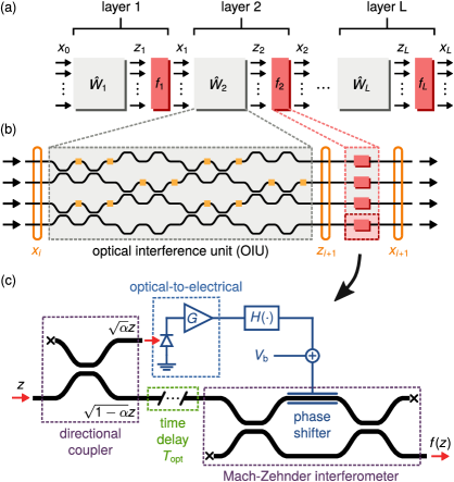
In this section, we briefly review the basics of feedforward artificial neural networks (ANNs) and describe their implementation in a reconfigurable optical circuit, as proposed in Ref. 12. As outlined in Fig. 1(a), an ANN is a function which accepts an input vector, and returns an output vector, . This is accomplished in a layer-by-layer fashion, with each layer consisting of a linear matrix-vector multiplication followed by the application of an element-wise nonlinear function, or activation, on the result. For a layer with index , containing a weight matrix and activation function , its operation is described mathematically as
| (1) |
for from 1 to .
Before they are able to perform a given machine learning task, ANNs must be trained. The training process is typically accomplished by minimizing the prediction error of the ANN on a set of training examples, which come in the form of input and target output pairs. For a given ANN, a loss function is defined to quantify the difference between the target output and output predicted by the network. During training, this loss function is minimized with respect to tunable degrees of freedom, namely the elements of the weight matrix within each layer. In general, although less common, it is also possible to train the parameters of the activation functions Trentin (2001).
Optical hardware implementations of ANNs have been proposed in various forms over the past few decades. In this work, we focus on a recent demonstration in which the linear operations are implemented using an integrated optical circuit Shen et al. (2017a). In this scheme, the information being processed by the network, , is encoded into the modal amplitudes of the waveguides feeding the device and the matrix-vector multiplications are accomplished using meshes of integrated optical interferometers. In this case, training the network requires finding the optimal settings for the integrated optical phase shifters controlling the inteferometers, which may be found using an analytical model of the chip, or using in-situ backpropagation techniques Hughes et al. (2018).
In the next section, we present an approach for realizing the activation function, , on-chip with a hybrid electro-optic circuit feeding an inteferometer. In Fig. 1(b), we show how this activation scheme fits into a single layer of an ONN and show the specific form of the activation in Fig. 1(c). We also give the specific mathematical form of this activation and analyze its performance in practical operation.
III Nonlinear Activation Function Architecture
In this section, we describe our proposed nonlinear activation function architecture for optical neural networks, which implements an optical-to-optical nonlinearity by converting a small portion of the optical input power into an electrical voltage. The remaining portion of the original optical signal is phase- and amplitude-modulated by this voltage as it passes through an interferometer. For an input signal with amplitude , the resulting nonlinear optical activation function, , is a result of the responses of the interferometer under modulation as well as the components in the electrical signal pathway.
A schematic of the architecture is shown in Fig. 1(c), where black and blue lines represent optical waveguides and electrical signal pathways, respectively. The input signal first enters a directional coupler which routes a portion, , of the input optical power to a photodetector. The photodetector is the first element of an optical-to-electrical conversion circuit, which is a standard component of high-speed optical receivers for converting an optical intensity into a voltage. In this work, we assume a normalization of the optical signal such that the total power in the input signal is given by . The optical-to-electrical conversion process consists of the photodetector producing an electrical current, , where is the photodetector responsivity, and a transimpedance amplifying stage, characterized by a gain , converting this current into a voltage . The output voltage of the optical-to-electrical conversion circuit then passes through a nonlinear signal conditioner with a transfer function, . This component allows for the application of additional nonlinear functions to transform the voltage signal. Finally, the conditioned voltage signal, is combined with a static bias voltage, to induce a phase shift of
| (2) |
for the optical signal routed through the lower port of the directional coupler. The parameter represents the voltage required to induce a phase shift of in the phase modulator. This phase shift, defined by Eq. 2, is a nonlinear self-phase modulation because it depends on the input signal intensity.
An optical delay line between the directional coupler and the Mach-Zehnder interferometer (MZI) is used to match the signal propagation delays in the optical and electrical pathways. This ensures that the nonlinear self-phase modulation defined by Eq. 2 is applied at the same time that the optical signal which generated it passes through the phase modulator. For the circuit shown in Fig. 1(c), the optical delay is , accounting for the contributions from the group delay of the optical-to-electrical conversion stage (), the delay associated with the nonlinear signal conditioner (), and the RC time constant of the phase modulator ().
The nonlinear self-phase modulation achieved by the electric circuit is converted into a nonlinear amplitude response by the MZI, which has a transmission depending on as
| (3) |
Depending on the configuration of the bias, , a larger input optical signal amplitude causes either more or less power to be diverted away from the output port, resulting in a nonlinear self-intensity modulation. Combining the expression for the nonlinear self-phase modulation, given by Eq. 2, with the MZI transmission, given by Eq. 3, the mathematical form of the activation function can be written explicitly as
| (4) |
where the contribution to the phase shift from the bias voltage is
| (5) |
For the remainder of this work, we focus on the case where no nonlinear signal conditioning is applied to the electrical signal pathway, i.e. . However, even with this simplification the activation function still exhibits a highly nonlinear response. We also neglect saturating effects in the OE conversion stage which can occur in either the photodetector or the amplifier. However, in practice, the nonlinear optical-to-optical transfer function could take advantage of these saturating effects.
With the above simplifications, a more compact expression for the activation function response is
| (6) |
where the phase gain parameter is defined as
| (7) |
Equation 7 indicates that the amount of phase shift per unit input signal power can be increased via the gain and photodiode responsivity, or by converting a larger fraction of the optical power to the electrical domain. However, tapping out a larger fraction optical power also results in a larger linear loss, which is undesirable.
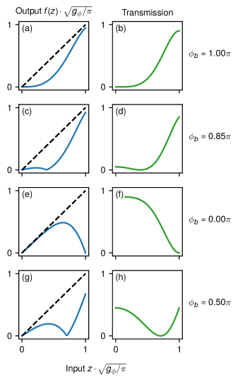
The electrical biasing of the activation phase shifter, represented by , is an important degree of freedom for determining its nonlinear response. We consider a representative selection, consisting of four different responses, in Fig. 2. The left column of Fig. 2 plots the output signal amplitude as a function of the input signal amplitude i.e. in Eq. 6, while the right column plots the transmission coefficient i.e. , a quantity which is more commonly used in optics than machine learning. The first two rows of Fig. 2, corresponding to and , exhibit a response which is comparable to the ReLU activation function: transmission is low for small input values and high for large input values. For the bias of , transmission at low input values is slightly increased with respect to the response where . Unlike the ideal ReLU response, the activation at is not entirely monotonic because transmission first goes to zero before increasing. On the other hand, the responses shown in the bottom two rows of Fig. 2, corresponding to and , are quite different. These configurations demonstrate a saturating response in which the output is suppressed for higher input values but enhanced for lower input values. For all of the responses shown in Fig. 2, we have assumed which limits the maximum transmission to .
A benefit of having electrical control over the activation response is that, in principle, its electrical bias can be connected to the same control circuitry which programs the linear interferometer meshes. In doing so, a single ONN hardware unit can then be reprogrammed to synthesize many different activation function responses. This opens up the possibility of heuristically selecting an activation function response, or directly optimizing the the activation bias using a training algorithm. This realization of a flexible optical-to-optical nonlinearity can allow ONNs to be applied to much broader classes of machine learning tasks.
We note that Fig. 2 shows only the amplitude response of the activation function. In fact, all of these responses also introduce a nonlinear self-phase modulation to the output signal. If desired, this nonlinear self-phase modulation can be suppressed using a push-pull interferometer configuration in which the generated phase shift, , is divided and applied with opposite sign to the top and bottom arms.
IV Performance and Scalability
In this section, we discuss the performance of an integrated ONN which uses meshes of integrated optical interferometers to perform matrix-vector multiplications and the electro-optic activation function, as shown in Fig. 1(b),(c). Here, we focus on characterizing how the power consumption, computational latency, physical footprint, and computational speed of the ONN scale with respect to the number of network layers, and the dimension of the input vector, , assuming square matrices. The system parameters used for this analysis are summarized in Table 1 and the figures of merit are summarized in Table 2.
| Parameter | Value |
|---|---|
| Modulator and detector rate | 10 GHz |
| Photodetector responsivity () | 1 A/W |
| Optical-to-electrical circuit power consumption | 100 mW |
| Optical-to-electrical circuit group delay () | 100 ps |
| Phase modulator RC delay () | 20 ps |
| Mesh MZI length | 100 m |
| Mesh MZI height | 60 m |
| Waveguide effective index () | 3.5 |
| Scaling | Per-layer figures of merit | ||||
|---|---|---|---|---|---|
| Mesh | Activation | ||||
| Power consumption∗ | 0.4 W | 1 W | 10 W | ||
| Latency | 125 ps | 132 ps | 237 ps | ||
| Footprint | 2.5 mm2 | 6.6 mm2 | 120.0 mm2 | ||
| Speed | MAC/s | MAC/s | MAC/s | ||
| Efficiency∗ | 2.5 pJ/MAC | 1 pJ/MAC | 100 fJ/MAC | ||
∗Assuming no power consumption in the interferometer mesh phase shifters
IV.1 Power consumption
The power consumption of the ONN, as shown in Fig. 1(b), consists of contributions from (1) the programmable phase shifters inside the interferometer mesh, (2) the optical source supplying the input vectors, , and (3) the active components of the activation function such as the amplifier and photodetector. In principle, the contribution from (1) can be made negligible by using phase change materials or ultra-low power MEMS phase shifters. Therefore, in this section we focus only on contributions (2) and (3) which pertain to the activation function.
To quantify the power consumption, we first consider the minimum input optical power to a single activation that triggers a nonlinear response. We refer to this as the activation function threshold, which is mathematically defined as
| (8) |
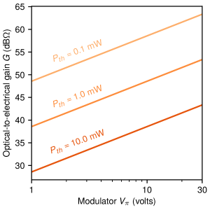
where is the is phase shift necessary to generate a 50% change in the power transmission with respect to the transmission with null input for a given . This threshold corresponds to in Fig. 2(b), to in Fig. 2(d), to in Fig. 2(f), and to in Fig. 2(h). In general, a lower activation threshold will result in a lower optical power required at the ONN input, . According to Eq. 8, the activation threshold can be reduced via a small and a large optical-to-electrical conversion gain, V/mW. The relationship between and for activation thresholds of 0.1 mW, 1.0 mW, and 10.0 mW is shown in Fig. 3 for a fixed = 1 A/W. Additionally, in Fig. 3 we conservatively assume which has the highest threshold of the activation function biases shown in Fig. 2.
If we take the lowest activation threshold of 0.1 mW in Fig. 3, the optical source to the ONN would then need to supply mW of optical power. The power consumption of integrated optical receiver amplifiers varies considerably, ranging from as low as 10 mW to as high as 150 mW Ahmed et al. (2014); Settaluri et al. (2017); Nozaki et al. (2018), depending on a variety of factors which are beyond the scope of this article. Therefore, a conservative estimate of the power consumption from the optical-to-electrical conversion circuits in all activations is mW. For an ONN with , the power consumption per layer from the activation function would be 10 W and would require a total optical input power of mW = 10 mW. Thus, the total power consumption of the ONN is dominated by the activation function electronics.
IV.2 Latency
For the feedforward neural network architecture shown in Fig. 1(a), the latency is defined by the elapsed time between supplying an input vector, and detecting its corresponding prediction vector, . In an integrated ONN, as implemented in Fig. 1(b), this delay is simply the travel time for an optical pulse through all -layers. Following Ref. 12, the propagation distance in a square interferometer mesh is , where is the length of each MZI within the mesh. In the nonlinear activation layer, the propagation length will be dominated by the delay line required to match the optical and electrical delays, and is given by
| (9) |
where the group velocity is the speed of optical pulses in the waveguide. Therefore,
| (10) |
Equation 10 indicates that the latency contribution from the interferometer mesh scales with the product , which is the same scaling as predicted in Ref. 12. On the other hand, the activation function adds to the latency independently of because each activation circuit is applied in parallel to all -vector elements.
For concreteness, we assume and . Following our assumption in the previous section of using no nonlinear electrical signal conditioner in the activation function, = 0 ps. Typical group delays for integrated transimpedance amplifiers used in optical receivers can range from 10 to 100 ps. Moreover, assuming an RC-limited phase modulator speed of 50 GHz yields ps. Therefore, if we assume a conservative value of = 100 ps, a network dimension of would have a latency of ps per layer, with equal contributions from the mesh and the activation function. For a ten layer network () the total latency would be approximately 2.4 ns, still orders of magnitude lower than the latency typically associated with GPUs.
IV.3 Physical footprint
The physical footprint of the ONN consists of the space taken up by both the linear interferometer mesh and the optical and electrical components of the activation function. Neglecting the electrical control lines for tuning each MZI, the total footprint of the ONN is
| (11) |
where is the area of a single MZI element in the mesh and is the area of a single activation function.
In the direction of propagation, is dominated by the waveguide optical delay line required to match the delay of the electrical signal pathway. Based on the previous discussion of the activation function’s latency, ps corresponds to a total waveguide length of 1 cm. For simplicity, we assume this delay is achieved using a straight waveguide, which results in a large footprint but with optical losses that can be very low. For example, in silicon waveguides losses below 0.5 dB/cm have been experimentally demonstrated Selvaraja et al. (2014). In principle, incorporating waveguide bends or resonant optical elements could significantly reduce the activation function’s footprint. For example, coupled micro ring arrays have experimentally achieved group delays of 135 ps over a bandwidth of 10 GHz in a 0.03 mm 0.25 mm footprint Cardenas et al. (2010).
Transverse to the direction of propagation, the activation function footprint will be dominated by the electronic components of the optical-to-electrical conversion circuit. In principle, compact waveguide photodetectors and modulators can be utilized. However, the components of the transimpedance amplifier may be challenging to integrate in the area available between neighboring output waveguides of the interferometer mesh. One possibility towards achieving a fully integrated opto-electronic ONN would be to use so-called amplifier-free optical receivers Nozaki et al. (2018), where ultra-low capacitance detectors provide high-speed opto-electronic conversion. Similarly to the experimental demonstration in Ref. 29, the amplifier-free receiver could be integrated directly with a high efficiency (e.g. effectively a low ) electro-optic modulator. Compact electro-absorption modulators could also be utilized. In addition to achieving a compact footprint, operating without an amplifier would also result in an order of magnitude reduction in both power consumption and latency, with the later reducing the required length of the optical delay line and thus the footprint.
For the purposes of our analysis, we assume no integration of the electronic transimpedance amplifier and, therefore, that the on-chip components of the activation function fit within the height of each interferometer mesh row, = 60 m. Under this assumption and following the scaling in Eq. 11, the total footprint of a single ONN layer of dimension would be 11.0 mm 0.6 mm. Interestingly, following the latency discussion in the previous section, a single ONN layer of dimension would have a footprint of 20.0 mm 6.0 mm, with equal contribution from the activation function and from the mesh.
IV.4 Speed
The speed, or computational capacity, of the ONN, as shown in Fig. 1(a), is determined by the number of input vectors, that can be processed per unit time. Here, we argue that although our activation function is not fully optical, it results in no speed degradation compared to a linear ONN consisting of only interferometer meshes.
The reason for this is that a fully integrated ONN would also include high-speed modulators and detectors on-chip to perform fast modulation and detection of sequences of vectors and vectors, respectively. We therefore argue that the same high-speed detector and modulator elements could also be integrated between the linear network layers to provide the optical-electrical and electrical-optical transduction for the activation function. State of the art integrated transimpedance amplifiers can already operate at speeds comparable to the optical modulator and detector rates, which are on the order of 50 - 100 GHz Yu et al. (2012); Ahmed et al. (2014), and thus would not be a limiting factor in the speed of our architecture.
To perform a matrix-vector multiplication on a conventional CPU requires multiply-accumulate (MAC) operations, each consisting of a single multiplication and a single addition. Therefore, assuming a photodetector and modulator rate of 10 GHz means that an ONN can effectively perform MAC/sec. This means that one layer of an ONN with dimension would effectively perform MAC/sec. Increasing the input dimension to would then scale the performance of the ONN to MAC/sec per layer. This is two orders of magnitude greater than the peak performance obtainable with modern GPUs, which typically have performance on the order of floating point operations/sec (FLOPS). Because the power consumption of the ONN scales as (assuming passive phase shifters in the mesh) and the speed scales as , the energy per operation is minimized for large (Table 2). Thus, for large ONNs the power consumption associated with the electro-optic conversion in the activation function can be amortized over the parallelized operation of the linear mesh.
We note that the activation function circuit shown in Fig. 1(c) can be modified to remove the matched optical delay line by using very long optical pulses. This modification may be advantageous for reducing the footprint of the activation and would result in . However, this results in a reduction of the ONN speed, which would then be limited by the combined activation delay of all nonlinear layers in the network, .
V Comparison with the Kerr Effect
All-optical nonlinearities such as bistability and saturable absorption have been previously considered as potential activation functions in ONNs Abu-Mostafa and Psaltis (1987); Shen et al. (2017b). An alternative implementation of the activation function in Fig. 1(c) could consist of a nonlinear MZI, with one of its arms having a material with Kerr nonlinear optical response. The Kerr effect is a third-order optical nonlinearity which generates a change in the refractive index, and thus a nonlinear phase shift, which is proportional to the input pulse intensity. In this section we compare the electro-optic activation function introduced in the previous section [Fig. 1(c)] to such an alternative all-optical activation function using the Kerr effect, highlighting how the electro-optic activation can achieve a lower activation threshold.
Unlike the electro-optic activation function, the Kerr effect is lossless and has no latency because it arises from a nonlinear material response, rather than a feedforward circuit. A standard figure of merit for quantifying the strength of the Kerr effect in a waveguide is through the amount of nonlinear phase shift generated per unit input power per unit waveguide length. This is given mathematically by the expression
| (12) |
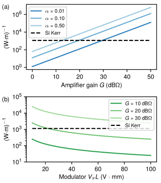
where is the nonlinear refractive index of the material and is the effective mode area. ranges from 100 (Wm)-1 in chalcogenide to 350 (Wm)-1 in silicon Koos et al. (2007). An equivalent figure of merit for the electro-optic feedforward scheme can be mathematically defined as
| (13) |
where is the phase modulator figure of merit. The figures of merit described in Eqs. 12-13 can be represented as an activation threshold (Eq. 8) via the relationship , for a given waveguide length, where the electro-optic phase shift or nonlinear Kerr effect take place.
A comparison of Eq. 12 and Eq. 13 indicates that while the strength of the Kerr effect is largely fixed by waveguide design and material choice, the electro-optic scheme has several degrees of freedom which allow it to potentially achieve a stronger nonlinear response. The first design parameter is the amount of power tapped off to the photodetector, which can be increased to generate a larger voltage at the phase modulator. However, increasing also increases the linear signal loss through the activation which does not contribute to the nonlinear mapping between the input and output of the ONN. Therefore, should be minimized as long as the optical power routed to the photodetector is large enough to be above the noise equivalent power level.
On the other hand, the product determines the conversion efficiency of the detected optical power into an electrical voltage. Fig. 4(a) compares the nonlinearity strength of the electro-optic activation (blue lines) to that of an implementation using the Kerr effect in silicon (black dashed line) for several values of , as a function of . The responsivity is fixed at A/W. We observe that tapping out 10% of the optical power requires a gain of 20 dB to achieve a nonlinear phase shift equivalent threshold to that of a silicon waveguide where = 0.05 m2 for the same amount of input optical power. Tapping out only 1% of the optical power requires an additional 10 dB of gain to maintain this equivalence. We note that the gain range considered in Fig. 4(a) is well within the regime of what has been demonstrated in integrated transimpedance amplifiers for optical receivers Ahmed et al. (2014); Settaluri et al. (2017); Nozaki et al. (2018). In fact, many of these systems have demonstrated much higher gain. In Fig. 4(a), the phase modulator was fixed at 20 Vmm. However, because a lower translates into an increased phase shift for a given applied voltage, this parameter can also be used to enhance the nonlinearity. Fig. 4(b) demonstrates the effect of changing the for several values of of , again, with a fixed responsivity A/W. This demonstrates that with a reasonable level of gain and phase modulator performance, the electro-optic activation function can trade off an increase in latency for a significantly lower optical activation threshold than the Kerr effect.
VI Machine Learning Tasks
In this section, we apply the electro-optic activation function introduced above to several machine learning tasks. In Sec. VI.1, we simulate training an ONN to implement an exclusive-OR (XOR) logical operation. The network is modeled using neuroptica noa , a custom ONN simulator written in Python, which trains the simulated networks only from physically measurable field quantities using the on-chip backpropagation algorithm introduced in Ref. 23. In Sec. VI.2, we consider the more complex task of using an ONN to classify handwritten digits from the Modified NIST (MNIST) dataset, which we model using the neurophox _ne ; Pai et al. (2019) package and tensorflow Abadi et al. (2015), which computes gradients using automatic differentiation. In both cases, we model the values in the network as complex-valued quantities and represent the interferometer meshes as unitary matrices parameterized by phase shifters.
VI.1 Exclusive-OR Logic Function
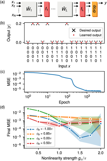
An exclusive-OR (XOR) is a logic function which takes two inputs and produces a single output. The output is high if only one of the two inputs is high, and low for all other possible input combinations. In this example, we consider a multi-input XOR which takes input values, given by , and produces a single output value, . The input-output relationship of the multi-input XOR function is a generalization of the two-input XOR. For example, defining logical high and low values as 1 and 0, respectively, a four-input XOR has an output table indicated the desired values in Fig. 5(b). We select this task for the ONN to learn because it requires a non-trivial level of nonlinearity, meaning that it could not be implemented in an ONN consisting of only linear interferometer meshes.
The architecture of the ONN used to learn the XOR is shown schematically in Fig. 5(a). The network consists of layers, with each layer constructed from an unitary interferometer mesh followed by an array of parallel electro-optic activation functions, with each element corresponding to the circuit in Fig. 1(c). After the final layer, the lower outputs are dropped to produce a single output value which corresponds to . Unlike the ideal XOR input-output relationship described above, for the XOR task learned by the ONN we normalize the input vectors such that they always have an norm of 1. This constraint is equivalent to enforcing a constant input power to the network. Additionally, because the activation function causes the optical power level to be attenuated at each layer, we take the high output state to be a value of 0.2, as shown in Fig. 1(b). The low output remains at a value of 0.0. An alternative to using a smaller amplitude for the output high state would be to add additional ports with fixed power biases to increase the total input power to the network, similarly to the XOR demonstrated in Ref. 23.
In Fig. 5(b) we show the four-input XOR input-output relationship which was learned by a two-layer ONN. The electro-optic activation functions were configured to have a gain of and biasing phase of . This biasing phase configuration corresponds to the ReLU-like response shown in Fig. 2(a). The black markers indicate the desired output values while the red circles indicate the output learned by the two-layer ONN. Fig. 5(b) indicates excellent agreement between the learned output and the desired output. The evolution of the mean squared error (MSE) between the ONN output and the desired output during training confirms this agreement, as shown in Fig. 5(c), with a final MSE below .
To train the ONN, a total of training examples were used, corresponding to all possible binary input combinations along the x-axis of Fig. 5(b). All 16 training examples were fed through the network in a batch to calculate the mean squared error (MSE) loss function. The gradient of the loss function with respect to each phase shifter was computed by backpropagating the error signal through the network to calculate the loss sensitivity at each phase shifter Hughes et al. (2018). The above steps were repeated until the MSE converged, as shown in Fig. 5(c). Only the phase shifter parameters were optimized by the training algorithm, while all parameters of the activation function were unchanged.
To demonstrate that the nonlinearity provided by the electro-optic activation function is essential for the ONN to successfully learn the XOR, in Fig. 5(d) we plot the final MSE after 5000 training epochs, averaged over 20 independent training runs, as a function of the activation function gain, . The shaded regions indicates the minimum and maximum range of the final MSE over the 20 training runs. The four lines shown in Fig. 5(d) correspond to the four activation function bias configurations shown in Fig. 2.
For the blue curve in Fig. 5(d), which corresponds to the ReLU-like activation, we observe a clear improvement in the final MSE with an increase in the nonlinearity strength. We also observe that for very high nonlinearity, above , the range between the minimum and maximum final MSE broadens and the mean final MSE increases. However, the best case (minimum) final MSE continues to decrease, as indicated by the lower border of the shaded blue region. This trend indicates that although increasing nonlinearity improves the ONN’s ability to learn the XOR function, very high levels of nonlinearity may also prevent the training algorithm from converging.
A trend of decreasing MSE with increasing nonlinearity is also observed for the activation corresponding to the green curve in Fig. 5(d). However, the range of MSE values begins to broaden at a lower value of . Such broadening may be a result of the changing slope in the activation function output, as shown in Fig. 2(e). For the activation functions corresponding to the red and orange curves in Fig. 5(d), the final MSE decreases somewhat with an increase in , but generally remains much higher than the other two activation function responses. We conclude that these two responses are not as well suited for learning the XOR function. Overall, these results demonstrate that the flexibility of our architecture to achieve specific forms of nonlinear activation functions is important for the successful operation of an ONN.
VI.2 Handwritten Digit Classification
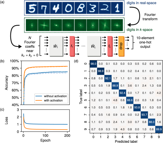
The second task we consider for demonstrating the activation function is classifying images of handwritten digits from the MNIST dataset, which has become a standard benchmark problem for ANNs Lecun et al. (1998). The dataset consists of 70,000 grayscale 2828 pixel images of handwritten digits between 0 and 9. Several representative images from the dataset are shown in Fig. 6(a).
To reduce the number of input parameters, and hence the size of the neural network, we use a preprocessing step to convert the images into a Fourier-space representation. Specifically, we compute the 2D Fourier transform of the images which is defined mathematically as , where is the gray scale value of the pixel at location within the image. The amplitudes of the Fourier coefficients are shown below their corresponding images in Fig. 6(a). These coefficients are generally complex-valued, but because the real-space map is real-valued, the condition applies.
We observe that the Fourier-space profiles are mostly concentrated around small and , corresponding to the center region of the profiles in Fig. 6(a). This is due to the slowly varying spatial features in the images. We can therefore expect that most of the information is carried by the small- Fourier components, and with the goal of decreasing the input size, we can restrict the data to coefficients with the smallest . An additional advantage of this preprocessing step is that it reduces the computational resources required to perform the training process because the neural network dimension does not need to accommodate all pixel values as inputs.
Fourier preprocessing is particularly relevant for ONNs for two reasons. First, the Fourier transform has a straightforward implementation in the optical domain using techniques from Fourier optics involving standard components such as lens and spatial filters Goodman (2005). Second, this approach allows us to take advantage of the fact that ONNs are complex-valued functions. That is to say, the complex-valued coefficients can be handled by an -dimensional ONN, whereas to handle the same input using a real-valued neural network requires a twice larger dimension. The ONN architecture used in our demonstration is shown schematically in Fig. 6(a). The Fourier coefficients closest to are fed into an optical neural network consisting of layers, after which a drop-mask reduces the final output to 10 components. The intensity of the 10 outputs are recorded and normalized by their sum, which creates a probability distribution that may be compared with the one-hot encoding of the digits from 0 to 9. The loss function is defined as the cross-entropy between the normalized output intensities and the correct one-hot vector.
During each training epoch, a subset of 60,000 images from the dataset were fed through the network in batches of 500. The remaining 10,000 image-label pairs were used to form a test dataset. For a two-layer network with Fourier components, Fig. 6(b) compares the classification accuracy over the training dataset (solid lines) and testing dataset (dashed lines) while Fig. 6(b) compares the cross entropy loss during optimization. The blue curves correspond to an ONN with no activation function (e.g. a linear optical classifier) and the orange curves correspond to an ONN with the electro-optic activation function configured with , , and . The gain setting in particular was selected heuristically. We observe that the nonlinear activation function results in a significant improvement to the ONN performance during and after training. The final validation accuracy for the ONN with the activation function is , which amounts to an 8% difference as compared to the linear ONN which achieved an accuracy of .
The confusion matrix computed over the testing dataset is shown in Fig. 6(d). We note that the prediction accuracy of is high considering that only complex Fourier components were used, and the network is parameterized by only free parameters. Moreover, this prediction accuracy is comparable with the accuracy achieved in a fully-connected linear classifier with 4010 free parameters taking all of the real-space pixel values as inputs Lecun et al. (1998). Finally, in Table 3 we show that the accuracy can be further improved by including a third layer in the ONN and by making the activation function gain a trainable parameter. This brings the testing accuracy to . Based on the parameters from Table 1 and the scaling from Table 2, the 3 layer handwritten digit classification system would consume 4.8 W while performing MAC/sec. Its prediction latency would be 1.5 ns.
| # Layers | Without activation | With activation | |
|---|---|---|---|
| Untrained | Trained∗ | ||
| 1 | 85.00% | 89.80% | 89.38% |
| 2 | 85.83% | 92.98% | 92.60% |
| 3 | 85.16% | 92.62% | 93.89% |
∗The phase gain, , of each layer was optimized during training
VII Conclusion
In conclusion, we have introduced an architecture for synthesizing optical-to-optical nonlinearities and demonstrated its use as a nonlinear activation function in a feed forward ONN. Using numerical simulations, we have shown that such activation functions enable an ONN to be successfully applied to two machine learning benchmark problems: (1) learning a multi-input XOR logic function, and (2) classifying handwritten numbers from the MNIST dataset. Rather than using all-optical nonlinearities, our activation architecture uses intermediate signal pathways in the electrical domain which are accessed via photodetectors and phase modulators. Specifically, a small portion of the optical input power is tapped out which undergoes analog processing before modulating the remaining portion of the same optical signal. Whereas all-optical nonlinearities have largely fixed responses, a benefit of the electro-optic approach demonstrated here is that signal amplification in the electronic domain can overcome the need for high optical signal powers to achieve a significantly lower activation threshold. For example, we show that a phase modulator of 10 V and an optical-to-electrical conversion gain of 57 dB, both of which are experimentally feasible, result in an optical activation threshold of 0.1 mW. We note that this nonlinearity is compatible with the in situ training protocol proposed in Ref. 23, which is applicable to arbitrary activation functions.
Our activation function architecture can utilize the same integrated photodetector and modulator technologies as the input and output layers of a fully-integrated ONN. This means that an ONN using this activation suffers no reduction in processing speed, despite using analog electrical components. The only trade off made by our design is an increase in latency due to the electro-optic conversion process. However, we find that an ONN with dimension has a total prediction latency of 2.4 ns/layer, with approximately equal contributions from the propagation of optical pulses through the interferometer mesh and from the electro-optic activation function. Conservatively, we estimate the energy consumption of an ONN with this activation function to be 100 fJ/MAC, but this figure of merit could potentially be reduced by orders of magnitude using highly efficient modulators and amplifier-free optoelectronics Nozaki et al. (2019).
Finally, we emphasize that in our activation function, the majority of the signal power remains in the optical domain. There is no need to have a new optical source at each nonlinear layer of the network, as is required in previously demonstrated electro-optic neuromorphic hardware Tait et al. (2017); Peng et al. (2018); Tait et al. (2019) and reservoir computing architectures Larger et al. (2012); Duport et al. (2016). Additionally, each activation function in our proposed scheme is a standalone analog circuit and therefore can be applied in parallel. While we have focused here on the application of our architecture as an activation function in a feedforward ONN, the synthesis of low-threshold optical nonlinearlities using this circuit could be of broader interest for optical computing as well as microwave photonic signal processing applications.
Acknowledgments
This work was supported by a US Air Force Office of Scientific Research (AFOSR) MURI project (Grant No FA9550-17-1-0002). I.A.D.W. acknowledges helpful discussions with Avik Dutt.
References
- Pallipuram et al. (2012) Vivek K. Pallipuram, Mohammad Bhuiyan, and Melissa C. Smith, “A comparative study of GPU programming models and architectures using neural networks,” The Journal of Supercomputing 61, 673–718 (2012).
- Shainline et al. (2017) Jeffrey M. Shainline, Sonia M. Buckley, Richard P. Mirin, and Sae Woo Nam, “Superconducting Optoelectronic Circuits for Neuromorphic Computing,” Physical Review Applied 7, 034013 (2017).
- Shastri et al. (2018) Bhavin J. Shastri, Alexander N. Tait, Thomas Ferreira de Lima, Mitchell A. Nahmias, Hsuan-Tung Peng, and Paul R. Prucnal, “Principles of Neuromorphic Photonics,” arXiv:1801.00016 [physics] , 1–37 (2018), arXiv:1801.00016 [physics] .
- Coarer et al. (2018) F. D. Coarer, M. Sciamanna, A. Katumba, M. Freiberger, J. Dambre, P. Bienstman, and D. Rontani, “All-Optical Reservoir Computing on a Photonic Chip Using Silicon-Based Ring Resonators,” IEEE Journal of Selected Topics in Quantum Electronics 24, 1–8 (2018).
- Chang et al. (2018) Julie Chang, Vincent Sitzmann, Xiong Dun, Wolfgang Heidrich, and Gordon Wetzstein, “Hybrid optical-electronic convolutional neural networks with optimized diffractive optics for image classification,” Scientific Reports 8, 12324 (2018).
- Colburn et al. (2019) Shane Colburn, Yi Chu, Eli Shilzerman, and Arka Majumdar, “Optical frontend for a convolutional neural network,” Applied Optics 58, 3179–3186 (2019).
- Capmany and Novak (2007) José Capmany and Dalma Novak, “Microwave photonics combines two worlds,” Nature Photonics 1, 319 (2007).
- Marpaung et al. (2013) David Marpaung, Chris Roeloffzen, René Heideman, Arne Leinse, Salvador Sales, and José Capmany, “Integrated microwave photonics,” Laser & Photonics Reviews 7, 506–538 (2013).
- Ghelfi et al. (2014) Paolo Ghelfi, Francesco Laghezza, Filippo Scotti, Giovanni Serafino, Amerigo Capria, Sergio Pinna, Daniel Onori, Claudio Porzi, Mirco Scaffardi, Antonio Malacarne, Valeria Vercesi, Emma Lazzeri, Fabrizio Berizzi, and Antonella Bogoni, “A fully photonics-based coherent radar system,” Nature 507, 341 (2014).
- Abu-Mostafa and Psaltis (1987) Yaser S. Abu-Mostafa and Demetri Psaltis, “Optical Neural Computers,” Scientific American 256, 88–95 (1987).
- Psaltis et al. (1990) Demetri Psaltis, David Brady, Xiang-Guang Gu, and Steven Lin, “Holography in artificial neural networks,” Nature 343, 325–330 (1990).
- Shen et al. (2017a) Yichen Shen, Nicholas C. Harris, Scott Skirlo, Mihika Prabhu, Tom Baehr-Jones, Michael Hochberg, Xin Sun, Shijie Zhao, Hugo Larochelle, Dirk Englund, and Marin Soljačić, “Deep learning with coherent nanophotonic circuits,” Nature Photonics 11, 441–447 (2017a).
- Miller (2013) David A. B. Miller, “Self-configuring universal linear optical component,” Photonics Research 1, 1 (2013).
- Tait et al. (2017) Alexander N. Tait, Thomas Ferreira de Lima, Ellen Zhou, Allie X. Wu, Mitchell A. Nahmias, Bhavin J. Shastri, and Paul R. Prucnal, “Neuromorphic photonic networks using silicon photonic weight banks,” Scientific Reports 7, 7430 (2017).
- Radulaski et al. (2018) Marina Radulaski, Ranojoy Bose, Tho Tran, Thomas Van Vaerenbergh, David Kielpinski, and Raymond G. Beausoleil, “Thermally Tunable Hybrid Photonic Architecture for Nonlinear Optical Circuits,” ACS Photonics 5, 4323–4329 (2018).
- Bao et al. (2011) Qiaoliang Bao, Han Zhang, Zhenhua Ni, Yu Wang, Lakshminarayana Polavarapu, Zexiang Shen, Qing-Hua Xu, Dingyuan Tang, and Kian Ping Loh, “Monolayer graphene as a saturable absorber in a mode-locked laser,” Nano Research 4, 297–307 (2011).
- Park et al. (2015) Nam Hun Park, Hwanseong Jeong, Sun Young Choi, Mi Hye Kim, Fabian Rotermund, and Dong-Il Yeom, “Monolayer graphene saturable absorbers with strongly enhanced evanescent-field interaction for ultrafast fiber laser mode-locking,” Optics Express 23, 19806 (2015).
- Jiang et al. (2018) Xiantao Jiang, Simon Gross, Michael J. Withford, Han Zhang, Dong-Il Yeom, Fabian Rotermund, and Alexander Fuerbach, “Low-dimensional nanomaterial saturable absorbers for ultrashort-pulsed waveguide lasers,” Optical Materials Express 8, 3055 (2018).
- Lentine and Miller (1993) A. L. Lentine and D. A. B. Miller, “Evolution of the SEED technology: Bistable logic gates to optoelectronic smart pixels,” IEEE Journal of Quantum Electronics 29, 655–669 (1993).
- Majumdar and Rundquist (2014) Arka Majumdar and Armand Rundquist, “Cavity-enabled self-electro-optic bistability in silicon photonics,” Optics Letters 39, 3864 (2014).
- Tait et al. (2019) Alexander N. Tait, Thomas Ferreira de Lima, Mitchell A. Nahmias, Heidi B. Miller, Hsuan-Tung Peng, Bhavin J. Shastri, and Paul R. Prucnal, “Silicon Photonic Modulator Neuron,” Physical Review Applied 11, 064043 (2019).
- Trentin (2001) Edmondo Trentin, “Networks with trainable amplitude of activation functions,” Neural Networks 14, 471–493 (2001).
- Hughes et al. (2018) Tyler W. Hughes, Momchil Minkov, Yu Shi, and Shanhui Fan, “Training of photonic neural networks through in situ backpropagation and gradient measurement,” Optica 5, 864–871 (2018).
- Ahmed et al. (2014) M. N. Ahmed, J. Chong, and D. S. Ha, “A 100 Gb/s transimpedance amplifier in 65 nm CMOS technology for optical communications,” in 2014 IEEE International Symposium on Circuits and Systems (ISCAS) (2014) pp. 1885–1888.
- Settaluri et al. (2017) K. T. Settaluri, C. Lalau-Keraly, E. Yablonovitch, and V. Stojanović, “First Principles Optimization of Opto-Electronic Communication Links,” IEEE Transactions on Circuits and Systems I: Regular Papers 64, 1270–1283 (2017).
- Nozaki et al. (2018) K. Nozaki, S. Matsuo, A. Shinya, and M. Notomi, “Amplifier-Free Bias-Free Receiver Based on Low-Capacitance Nanophotodetector,” IEEE Journal of Selected Topics in Quantum Electronics 24, 1–11 (2018).
- Selvaraja et al. (2014) Shankar Kumar Selvaraja, Peter De Heyn, Gustaf Winroth, Patrick Ong, Guy Lepage, Celine Cailler, Arnaud Rigny, Konstantin K. Bourdelle, Wim Bogaerts, Dries Van Thourhout, Joris Van Campenhout, and Philippe Absil, “Highly uniform and low-loss passive silicon photonics devices using a 300mm CMOS platform,” in Optical Fiber Communication Conference (2014), Paper Th2A.33 (Optical Society of America, 2014) p. Th2A.33.
- Cardenas et al. (2010) Jaime Cardenas, Mark A. Foster, Nicolás Sherwood-Droz, Carl B. Poitras, Hugo L. R. Lira, Beibei Zhang, Alexander L. Gaeta, Jacob B. Khurgin, Paul Morton, and Michal Lipson, “Wide-bandwidth continuously tunable optical delay line using silicon microring resonators,” Optics Express 18, 26525 (2010).
- Nozaki et al. (2019) Kengo Nozaki, Shinji Matsuo, Takuro Fujii, Koji Takeda, Akihiko Shinya, Eiichi Kuramochi, and Masaya Notomi, “Femtofarad optoelectronic integration demonstrating energy-saving signal conversion and nonlinear functions,” Nature Photonics (2019), 10.1038/s41566-019-0397-3.
- Yu et al. (2012) G. Yu, X. Zou, L. Zhang, Q. Zou, M. zheng, and J. Zhong, “A low-noise high-gain transimpedance amplifier with high dynamic range in 0.13ìm CMOS,” in 2012 IEEE International Symposium on Radio-Frequency Integration Technology (RFIT) (2012) pp. 37–40.
- Shen et al. (2017b) Yichen Shen, Nicholas C. Harris, Scott Skirlo, Mihika Prabhu, Tom Baehr-Jones, Michael Hochberg, Xin Sun, Shijie Zhao, Hugo Larochelle, Dirk Englund, and Marin Soljačić, “Supplementary information: Deep learning with coherent nanophotonic circuits,” Nature Photonics 11, 441–446 (2017b).
- Koos et al. (2007) C. Koos, L. Jacome, C. Poulton, J. Leuthold, and W. Freude, “Nonlinear silicon-on-insulator waveguides for all-optical signal processing,” Optics Express 15, 5976–5990 (2007).
- (33) “Neuroptica: An optical neural network simulator,” https://github.com/fancompute/neuroptica/.
- (34) “Neurophox: A simulation framework for unitary neural networks and photonic devices,” https://github.com/solgaardlab/neurophox/.
- Pai et al. (2019) Sunil Pai, Ben Bartlett, Olav Solgaard, and David A. B. Miller, “Matrix Optimization on Universal Unitary Photonic Devices,” Physical Review Applied 11, 064044 (2019).
- Abadi et al. (2015) Martín Abadi, Ashish Agarwal, Paul Barham, Eugene Brevdo, Zhifeng Chen, Craig Citro, Greg S. Corrado, Andy Davis, Jeffrey Dean, Matthieu Devin, Sanjay Ghemawat, Ian Goodfellow, Andrew Harp, Geoffrey Irving, Michael Isard, Yangqing Jia, Rafal Jozefowicz, Lukasz Kaiser, Manjunath Kudlur, Josh Levenberg, Dandelion Mané, Rajat Monga, Sherry Moore, Derek Murray, Chris Olah, Mike Schuster, Jonathon Shlens, Benoit Steiner, Ilya Sutskever, Kunal Talwar, Paul Tucker, Vincent Vanhoucke, Vijay Vasudevan, Fernanda Viégas, Oriol Vinyals, Pete Warden, Martin Wattenberg, Martin Wicke, Yuan Yu, and Xiaoqiang Zheng, “TensorFlow: Large-Scale Machine Learning on Heterogeneous Systems,” (2015), software available from tensorflow.org.
- Lecun et al. (1998) Y. Lecun, L. Bottou, Y. Bengio, and P. Haffner, “Gradient-based learning applied to document recognition,” Proceedings of the IEEE 86, 2278–2324 (1998).
- Goodman (2005) Joseph W. Goodman, Introduction to Fourier Optics (Roberts and Company Publishers, 2005).
- Peng et al. (2018) H. Peng, M. A. Nahmias, T. F. de Lima, A. N. Tait, and B. J. Shastri, “Neuromorphic Photonic Integrated Circuits,” IEEE Journal of Selected Topics in Quantum Electronics 24, 1–15 (2018).
- Larger et al. (2012) L. Larger, M. C. Soriano, D. Brunner, L. Appeltant, J. M. Gutierrez, L. Pesquera, C. R. Mirasso, and I. Fischer, “Photonic information processing beyond Turing: An optoelectronic implementation of reservoir computing,” Optics Express 20, 3241 (2012).
- Duport et al. (2016) François Duport, Anteo Smerieri, Akram Akrout, Marc Haelterman, and Serge Massar, “Fully analogue photonic reservoir computer,” Scientific Reports 6, 22381 (2016).