-
December 2018
Dry transfer method for suspended graphene on lift-off-resist: simple ballistic devices with Fabry-Pérot interference
Abstract
We demonstrate a fabrication scheme for clean suspended structures using chemical-vapor-deposition-grown graphene and a dry transfer method on lift-off-resist-coated substrates to facilitate suspended graphene nanoelectronic devices for technology applications. It encompasses the demands for scalable fabrication as well as for ultra-fast response due to weak coupling to environment. The fabricated devices exhibited initially a weak field-effect response with substantial positive () doping which transformed into weak negative () doping upon current annealing at the temperature of 4 Kelvin. With increased annealing current, -doping gradually decreased while the Dirac peak position approached zero in gate voltage. An ultra-low residual charge density of and a mobility of were observed. Our samples display clear Fabry-Pérot (FP) conductance oscillation which indicates ballistic electron transport. The spacing of the FP oscillations are found to depend on the charge density in a manner that agrees with theoretical modeling based on Klein tunneling of Dirac particles. The ultra-low residual charge, the FP oscillations with density dependent period, and the high mobility prove excellent quality of our suspended graphene devices. Owing to its simplicity, scalability and robustness, this fabrication scheme enhances possibilities for production of suspended, high-quality, two-dimensional-material structures for novel electronic applications.
Keywords: quantum technology, suspended graphene, ballistic transport, current annealing, negative doping, Fabry-Pérot interference
1 Introduction
Suspended graphene devices with attractive mechanical and electronic properties have been utilized during the past few years as a playground for fundamental physics and as a platform for novel electronic applications[1]. Recent fractional quantum Hall effect experiments [2, 3], electron-optic[4], electron-phonon interaction measurements [5, 6] and several ballistic transport studies [7, 8, 9, 10] have employed high-quality suspended graphene samples. These devices act also as nanoelectromechanical systems (NEMS) [11], which facilitate e.g. tunable mechanical resonators [12, 13], radio frequency components [14], as well as ultra-sensitive sensors for mass and force [15, 16].
The conventional fabrication method for making suspended graphene devices [8, 17] involves exfoliation of graphene onto a Si/SiO2 substrate, followed by patterning of the contacts. Subsequent wet etching of SiO2 in buffered hydrofluoric acid (BHF) is used to release and suspend the graphene structure. After isotropic SiO2 etching, the graphene device is prone to collapse, which reduces yield of the fabrication process. Furthermore, reactivity of several metals with BHF limits material choices for the electrical contacts to graphene; even with less reactive metals, BHF etch may compromise the overall electrical characteristics of the graphene device by degrading the contact performance.
Several works [5, 18, 19] have demonstrated fabrication of suspended graphene devices using polydimethylglutarimide (PMGI) based Lift-Off-Resist (LOR) as a sacrificial layer instead of the conventional SiO2. This method provides a large yield, and it is also compatible with commonly used contact materials for graphene. In this work, we too employed LOR as a supporting layer for CVD-grown (Chemical Vapor Deposition) graphene which was deposited using an optimized dry transfer method for transferring isolated flakes of graphene. Comprehensive measurements on the effect of current annealing on the device quality were carried out. Electrical transport at sub-Kelvin temperatures was performed in order to verify the high quality of our suspended CVD-graphene devices.
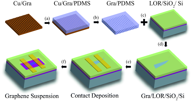
2 Device Fabrication Process
The fabrication process flow is schematically depicted in figure 1. First, a polydimethylsiloxane (PDMS) stamp was prepared and the graphene on copper foil was placed on the PDMS stamp with the graphene face down. The copper foil was gently pressed onto the stamp in order to make graphene to adhere well to PDMS. The Cu/graphene/PDMS stamp was placed in Cu etchant (1M FeCl3) to remove the copper, followed by repeated rinsing in deionized water. To further remove etch residues from the graphene surface, the graphene-PDMS stamp was cleaned using the modified RCA method [20]. The substrate for graphene transfer was prepared by spin coating two layers of LOR-3A resist (PMGI based organic polymer from MicroChem) on silicon substrate capped with 285-nm-thick SiO2. Each LOR layer resulted in a thickness of about 250 nm. The cleaned Graphene-PDMS stamp and the LOR coated substrate were then mounted onto a home-made dry transfer setup.
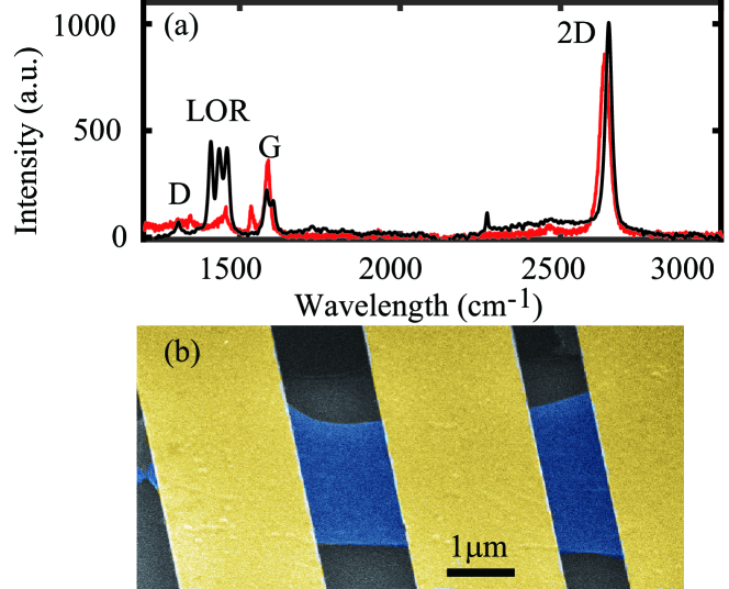
The stamp was next aligned and brought into contact with the substrate, after which the stamp was peeled off of the substrate. When the stamp was peeled off slowly, uninterrupted graphene transfer could be achieved leading to the graphene covering the entire substrate. We note that this could be useful for larger scale fabrication of suspended graphene device arrays by introducing additional patterning and etching steps. On the other hand, when the stamp was immediately peeled off of the substrate with a high speed, then only small cracked flakes from continuous graphene film transferred due to incomplete adhesion to the substrate. Since these well-isolated graphene flakes could be immediately used for making suspended devices of size that can survive the suspension process without extra patterning and etching steps, we focus on them in the following experiments and analysis. Monolayer graphene flakes with suitable sizes were located using an optical microscope, followed by micro-Raman measurements as illustrated in figure 2a. Signatures of graphene’s characteristic Raman peaks labeled as D, 2D and G were observed, together with a LOR peak between the D and G peaks of graphene. The CVD graphene used here was foremost made of monolayer, but small patches of bi-layer were present. The bilayer regions resulted in darker optical contrast and the difference between mono and bi-layer could be easily distingushed using optical microscopy.
Two layers of polymethylmethacrylate (PMMA) (top most layer of 950K/A3, bottom layer of 50K/A11) was spin coated on the graphene/LOR chip for standard electron beam lithography. The lithography was operated under accelerating voltage. An electron beam dose of was employed to pattern the electrical leads. To enhance the selectivity of the development of the PMMA resist on top of LOR, the samples were developed in xylene instead of the regular developer methylisobutylketone (MIBK). The electrical leads were made by evaporating a Cr/Au bilayer with thickness 5/65 nm, respectively. The lift off process after evaporation was performed at 80 in xylene. To release and suspend graphene, the LOR underneath the graphene and the metal contact regions was exposed to electron beam irradiation with a dose of , which allowed removal of the exposed LOR by immersing the sample in ethyl lactate. After rinsing in hexane, the sample was finally taken out from the low-surface-tension solvent and blown dry gently using N2 gas. Figure 2b, shows a false color Scanning Electron Microscope (SEM) image of one of the fabricated devices.
3 Results and discussion
The electronic transport measurements were conducted in a Bluefors LD250 dilution refrigerator. The devices were electrically characterized by measuring source-drain resistance as a function of back-gate bias with a fixed source-drain voltage. The gating curve of the as-fabricated device is shown as the red resistance trace in figure 3; the inset displays a blow-up of the as-fabricated behavior. The absence of the Dirac peak and just a weak field effect (see the inset) indicate strong positive doping (-doping). Similar findings have been obtained in several other experiments [18, 21, 22, 23, 24, 25, 26, 27], and they have usually been attributed to PMMA residues from the fabrication processes [23, 24, 25] or ambient adsorbates like O2, H2O [26, 27]. In our work, low-temperature current annealing was performed to remove contaminants and to improve surface quality of graphene as described in reference [3]. We measured the resistance of the device as a function of the applied gate voltage after each annealing cycle. Upon current annealing, we see that the position of the Dirac point shifts to negative indicating -doping, which is against the expected -doping of graphene by PMMA residues. If PMMA as such were the -dopant, then the device should consistently display -doping until PMMA residues are completely removed. Intermediate-stage -doping during annealing has also previously been observed in similar structures [28, 29, 30].
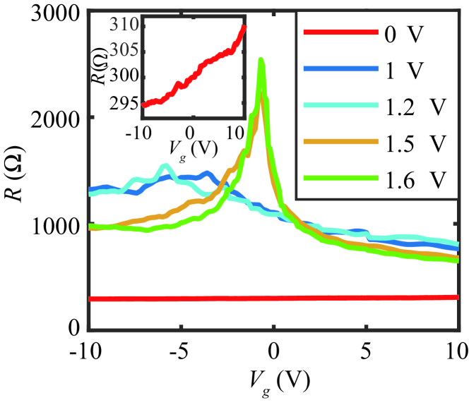
Instead of acting as an important -doping source, PMMA residue is expected to play a neutral, benign role [31, 32] in establishing electrical properties of graphene. However, a reasonable explanation for the observed -doping could be hydrogenation of graphene by H and low-molecular-weight hydrocarbon radicals released from the PMMA decomposition [33, 34, 35]. These light and H-rich radicals released by resist induce the hydrogenation of graphene, which results in the -doping at intermediate stages of the current annealing.
In order to understand the possible origin of H-rich radicals, let us first discuss the doping in samples on SiO2 substrates. As is well known, pristine graphene surface is hydrophobic [36] and can hardly adsorb O2 or H2O molecules [37, 38]. However, -doping can be created by O2 and H2O that are adsorbed between graphene and SiO2 interface, and are bonded by hydrogen bond with Si-OH on the surface of SiO2 in on-substrate graphene devices. This picture of doping has been verified by several experiments [22, 37, 38, 39].
In suspended graphene devices, we argue that the PMMA residue forms - before it is fully removed - a layer which plays a role similar to the SiO2 for the adsorption of O2, H2O molecules. The initial -doping observed in figure 3 would then originate from the dissolution of O2, H2O in the PMMA residue (or PMMA/graphene interface) rather than direct adsorption on the graphene surface. During current annealing, the graphene sheet heats up, which leads to evaporation of O2 and H2O molecules as well as decomposition of PMMA residues with the accompanying creation of H and low-molecular-weight hydrocarbon radicals. As a result, the -doping in graphene gradually weakens and -doping emerges. As the annealing process continues, the graphene sheet recovers its nearly pristine, undoped characteristics, which is implied by the position of the Dirac peak at V (figure 3).
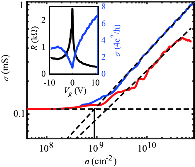
The ideal conductivity of a graphene device arises from mode-dependent, transmission probabilities of massless Dirac fermions [42, 43], which leads to a minimum . In order to compare our results with theory, we subtract a contact resistance of 560 which guarantees a correct asymptotic behavior of at large of our electron side data. The reduced device resistance and the corresponding conductivity as a function of are shown by the black and blue curves in the inset of figure 4, respectively. The minimum conductivity of our sample amounts to , where . This result is close to other experimental results on high-quality graphene (see e.g. reference [8]). For electron mobility we obtain from the Drude model () applied at carrier density of , slightly above the cross-over point, above which the gate doping becomes effective. Normalized by the length of graphene, our mobility is quite comparable to the reported results from equally-sized graphene devices encapsulated inside hexagonal boron nitride [44].
Figure 4 shows our measured graphene conductivity as a function of charge carrier density on log-log scale. The red and blue curves correspond to the hole and electron transport, respectively. The residual charge density is extracted below the cross-over point at which the conductivity levels off when approaching the Dirac point. The two curves are fitted using the power-law form , with the exponent close to . For the hole transport data, the existence of interfaces at the edges results in a -dependent series resistance which is difficult to subtract away with good accuracy. Thus, the residual charge density eventually is evaluated from the electron side data as this unipolar regime is less complex. At the cross-over point, an ultra-low residual charge density of is obtained, which is close to that of exfoliated graphene devices [3, 8, 10]. Thus, the main issue for high-quality in the suspended geometry is not the source of the graphene, but the successful current annealing.
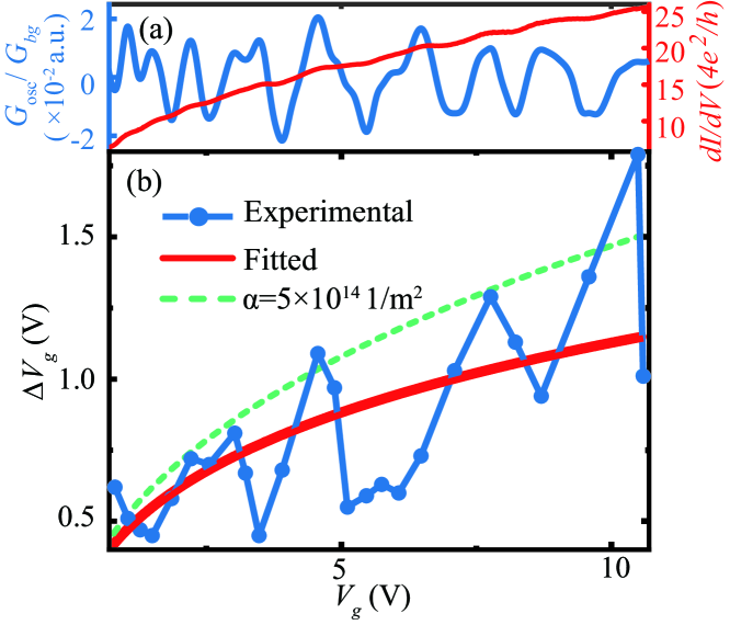
On top of the smooth varying background conductance, we observe fast-oscillating Fabry-Pérot-interference-induced modulation of the differential conductance that is displayed in figure 5a. The red curve displays the differential conductance at the doping side where a clear oscillation riding on the increasing conductance curve can be seen. To extract the oscillations, we employ an advanced adaptive algorithm [45] which effectively separates the smooth, sloped background and the oscillations . The resulting relative oscillation , shown in blue in figure 5a, originates from Fabry-Pérot interference within the cavity delineated by strongly modulated doping regions at the edges [40, 46, 47]. In our graphene device, sharp interfaces are formed between the graphene underneath the contact and the suspended region. The observed, well-developed FP oscillations in figure 5a indicate that the electron transport in our sample takes place ballistically [5, 8, 9, 44].
The FP oscillation periods in gate voltage can be extracted from the trace in figure 5a. The obtained is displayed as a function of by the blue joined circles in figure 5b. According to reference [40, 41], the oscillation period obeys
| (1) |
where is the length of the graphene stripe, is the specific capacitance of the gate electrode, the barrier parameter is governed by the slope of the electrostatic potential in the junction region with spatially varying doping, and denotes Planck’s constant. Trapeziodal potential barrier with height together with linearly varying edges over distance yields , where the parameter is the Fermi electric flux [40, 41]. A fit of equation 1 to the data is illustrated by the red curve in figure 5b which yields . This value for is within a factor of from the result of suspended device fabricated using exfoliated graphene on Si/SiO2 substrate [41], which yields at . Even though there is some discrepancy, the theoretical result (dashed green curve) of equation 1 with is still within the scatter of our experimental data. The disagreement is presumably due to variation in the trapezoidal barrier caused by a difference in the contact doping due to the chosen Au/Cr/Au ratios of the contact metal structures.
4 Summary
We have demonstrated a simple fabrication scheme for suspending two-dimensional (2D) materials with a high success rate achieved by combining CVD graphene and a clean dry transfer method on LOR-coated substrates. The shift of the Dirac peak upon current annealing was systematically monitored and the observed behavior was attributed to hydrogenation of graphene by H and low-molecular-weight hydrocarbon radicals. Transport measurement results in our devices indicate a low residual charge density of . Our samples display a mobility of and clear FP oscillations, which indicates nearly pristine graphene behavior with ballistic electron transport. The proposed fabrication methods hold remarkable potential for the development of technological applications using suspended structures of 2D materials.
Referencing
References
- [1] Ferrari A C, Bonaccorso F, Falḱo V, Novoselov K S, Roche S, Bøggild P, Borini S, Koppens F H L, Palermo V, Pugno N, Garrido J a, Sordan R, Bianco A, Ballerini L, Prato M, Lidorikis E, Kivioja J, Marinelli C, Ryhänen T, Morpurgo A, Coleman J N, Nicolosi V, Colombo L, Fert A, Garcia-Hernandez M, Bachtold A, Schneider G F, Guinea F, Dekker C, Barbone M, Sun Z, Galiotis C, Grigorenko A N, Konstantatos G, Kis A, Katsnelson M, Vandersypen L, Loiseau A, Morandi V, Neumaier D, Treossi E, Pellegrini V, Polini M, Tredicucci A, Williams G M, Hee Hong B, Ahn J H, Min Kim J, Zirath H, van Wees B J, van der Zant H, Occhipinti L, Di Matteo A, Kinloch I a, Seyller T, Quesnel E, Feng X, Teo K, Rupesinghe N, Hakonen P, Neil S R T, Tannock Q, Löfwander T and Kinaret J 2015 Nanoscale 7 4598
- [2] Bolotin K I, Ghahari F, Shulman M D, Stormer H L and Kim P 2009 Nature 462 196
- [3] Kumar M, Laitinen A and Hakonen P J 2018 Nat. Commun. 9 2776
- [4] Rickhaus P, Makk P, Liu M H, Richter K and Schönenberger C 2015 Appl. Phys. Lett. 107 251901
- [5] Rickhaus P, Maurand R, Liu M H, Weiss M, Richter K and Schönenberger C 2013 Nat. Commun. 4 2342
- [6] Laitinen A, Oksanen M, Fay A, Cox D J, Tomi M, Virtanen P and Hakonen P J 2014 Nano Lett. 14 3009–3013
- [7] Bolotin K I, Sikes K J, Hone J, Stormer H L and Kim P 2008 Phys. Rev. Lett. 101 096802
- [8] Du X, Skachko I, Barker A and Andrei E Y 2008 Nat. Nanotech. 3 491
- [9] Oksanen M, Uppstu A, Laitinen A, Cox D J, Craciun M F, Russo S, Harju A and Hakonen P J 2014 Phys. Rev. B 89 121414
- [10] Kumaravadivel P and Du X 2016 Sci. Rep. 6 24274
- [11] Bunch J S, Van-Der-Zande A M, Verbridge S S, Frank I W, Tanenbaum D M, Parpia J M, Craighead H G and McEuen P L 2007 Science 315 490–493
- [12] Chen C Y, Lee S, Deshpande V V, Lee G H, Lekas M, Shepard K and Hone J 2013 Nat. Nanotech. 8 923
- [13] De Alba R, Massel F, Storch I R, Abhilash T S, Hui A, McEuen P L, Craighead H G and Parpia J M 2016 Nat. Nanotech. 11 741
- [14] Song X F, Oksanen M, Sillanpää M A, Craighead H G, Parpia J M and Hakonen P J 2011 Nano Lett. 12 198–202
- [15] Eichler A, Moser J, Chaste J, Zdrojek M, Wilson-Rae I and Bachtold A 2011 Nat. Nanotech. 6 339
- [16] Weber P, Güttinger J, Noury A, Vergara-Cruz J and Bachtold A 2016 Nat. Commun. 7 12496
- [17] Bolotin K I, Sikes K J, Jiang Z G, Klima M, Fudenberg G, Hone J, Kim P and Stormer H L 2008 Solid State Commun. 146 351
- [18] Tombros N, Veligura A, Junesch J, Jasper Van Den Berg J, Zomer P J, Wojtaszek M, Vera Marun I J, Jonkman H T and Van Wees B J 2011 J. Appl. Phys. 109 093702
- [19] Grushina A L, Ki D K and Morpurgo A F 2013 Appl. Phys. Lett. 102 223102
- [20] Liang X L, Sperling B A, Calizo I, Cheng G J, Hacker C A, Zhang Q, Obeng Y, Yan K, Peng H L, Li Q L, Zhu X, Yuan H, Hight Walker A R, Liu Z, Peng L m and Richter C A 2011 ACS Nano 5 9144
- [21] Tombros N, Veligura A, Junesch J, Guimarães M H, Vera Marun I J, Jonkman H T and Van Wees B J 2011 Nat. Phys. 7 697
- [22] Pirkle A, Chan J, Venugopal A, Hinojos D, Magnuson C W, McDonnell S, Colombo L, Vogel E M, Ruoff R S and Wallace R M 2011 Appl. Phys. Lett. 99 122108
- [23] Suk J W, Lee W H, Lee J, Chou H, Piner R D, Hao Y F, Akinwande D and Ruoff R S 2013 Nano Lett. 13 1462
- [24] Kumar K, Kim Y S and Yang E H 2013 Carbon 65 35
- [25] Kumar P and Kumar A 2014 Appl. Phys. Lett. 104 083517
- [26] Yang Y X, Brenner K and Murali R 2012 Carbon 50 1727
- [27] Romero H E, Shen N, Joshi P, Gutierrez H R, Tadigadapa S A, Sofo J O and Eklund P C 2008 ACS Nano 2 2037
- [28] Mizuno N, Nielsen B and Du X 2013 Nat. Commun. 4 2716
- [29] Grushina A 2015 Quantum transport in high quality suspended graphene Ph.D. thesis University of Geneva
- [30] Chen W, Yu Y Y, Zheng X M, Qin S Q, Wang F, Fang J Y, Wang G, Wang C C, Wang L, Peng G and Zhang X A 2015 Sci. Rep. 5 12198
- [31] Gammelgaard L, Caridad J M, Cagliani A, Mackenzie D M A, Petersen D H, Booth T J and Bøggild P 2014 2D Mater. 1 035005
- [32] Koo E and Ju S Y 2015 Carbon 86 318
- [33] Ryu S, Han M Y, Maultzsch J, Heinz T F, Kim P, Steigerwald M L and Brus L E 2008 Nano Lett. 8 4597
- [34] Ennis C P and Kaiser R I 2010 Phys. Chem. Chem. Phys. 12 14902
- [35] Kim B H, Hong S J, Baek S J, Jeong H Y, Park N, Lee M, Lee S W, Park M, Chu S W, Shin H S, Lim J, Lee J C, Jun Y and Park Y W 2012 Sci. Rep. 2 690
- [36] Leenaerts O, Partoens B and Peeters F M 2009 Phys. Rev. B 79 235440
- [37] Ryu S, Liu L, Berciaud S, Yu Y J, Liu H, Kim P, Flynn G W and Brus L E 2010 Nano Lett. 10 4944
- [38] Xu H, Chen Y B, Zhang J and Zhang H L 2012 Small 8 2833
- [39] Pinto H and Markevich A 2014 Beilstein J. Nanotech. 5 1842
- [40] Sonin E B 2009 Phys. Rev. B 79 195438
- [41] Laitinen A, Paraoanu S, Oksanen M, Craciun M F, Russo S, Sonin E B and Hakonen P J 2016 Phys. Rev. B 93 115413
- [42] Katsnelson M 2006 Eur. Phys. J. B 51 157
- [43] Tworzydło J, Trauzettel B, Titov M, Rycerz A and Beenakker C W J 2006 Phys. Rev. Lett. 96 246802
- [44] Shalom M B, Zhu M, Falḱo V, Mishchenko A, Kretinin A, Novoselov K, Woods C, Watanabe K, Taniguchi T, Geim A and Prance J R 2016 Nat. Phys. 12 318
- [45] Huang N E, Shen Z, Long S R, Wu M C, Shih H H, Zheng Q, Yen N C, Chi C T and Liu H H 1998 Proc. Royal Soc. A 454 903–995
- [46] Cheianov V V and Falḱo V I 2006 Phys. Rev. B 74 1403
- [47] Gunlycke D and White C T 2008 Appl. Phys. Lett. 93 665