Layertronic control of topological states in multilayer metal-organic frameworks
Abstract
We investigate the layer localization control of two-dimensional states in multilayer metal-organic frameworks (MOFs). For finite stackings of (NiC4S MOFs, the weak van der Waals coupling between adjacent layers leads to a Fermi level dependent distribution of the electronic states in the monolayers. Such distribution is reflected in the topological edge states of multilayer nanoribbons. Moreover, by applying an external electric field, parallel to the stacking direction, the spacial localization of the electronic states can be controlled for a chosen Fermi energy. This localization behavior is studied comparing density functional theory calculations with a kagome lattice tight-binding model. Furthermore, for infinite stacked nanoribbons, a new V-gutter Dirac state is found in the side surfaces, which allows anisotropic current control by tuning the Fermi energy. Our results can be immediately extended to other kagome MOFs with eclipsed stackings, introducing a new degree of freedom (layer localization) to materials design.
I Introduction
Two-dimensional topological insulators (2DTI) have attracted broad interest for novel applications due to their characteristic dissipationless transport properties [1; 2]. While graphene was the first predicted 2DTI, its topological gap is too small to be observed experimentally [3; 4]. Recently, a new class of large gap 2D topological materials, the metal-organic frameworks (MOFs), emerged as an ideal playground to achieve different properties. That is mainly due to a rich tunability of MOFs via different combinations of metals and organic ligands to form designed materials with selected properties [5; 6; 7; 8; 9; 10]. For instance, it has been shown that Mn, Fe and Co-bis(dithiolene) are ferromagnetic half-metals, while n-doped Ru-bis(dithiolene) has a large gap Quantum Anomalous Hall phase [11; 12]. On the other hand, by keeping iron as the metal and changing the organic ligand to a coronene based molecule, a ferromagnetic semicondutor phase has been found [13]. Currently, a great number of MOFs are predicted to host topological phases [14; 15; 16; 17; 18; 19; 20; 21; 22]. Within these materials, nickel and palladium-bis(dithiolene) monolayers were experimentally synthesized [23; 24], and theoretically shown to host a 2DTI phase for n-doped systems [25]. Although the monolayer system need to be n-doped to achieve the 2DTI phase, in a recent work we have shown that for bilayers of nickel and platinum-bis(dithiolene), the topological gap falls onto the Fermi level [26].
The development of novel nano-devices based on 2DTIs is linked to the experimental control of its properties, and manipulation of its charge, spin and valley degrees of freedom [27; 28]. Recently, it has been proposed a bending strain perturbation approach to control spin currents in 2DTIs [29]. Meanwhile, ensuing research has shown layer localization control of topological states by an applied external electric field in MOF bilayer nanoribbons [26] and bilayer graphene grain boundaries [30]. Furthermore, the exploration of van de Waals heterostructures allows for designed properties by combining the stacking of two-dimensional materials [31; 32]. Within the heterostructures, the number of stacked layers and the stacking order has great impact in the electronic properties [33; 34; 35]. Therefore, in order to control the electronic properties of MOFs multilayer, a clear understanding of its stacking is required.
In this paper, we study the stability and control of the electronic properties of the MOF (NiC4S stacking, from a monolayer to the bulk limit. Our first-principles results show that the mirror symmetric AA stacking is the most stable configuration. For a finite AA stacking, each layer corresponds to a 2DTI system with helical edge states weakly coupled to its counterpart in adjacent layers. Here, the edge states are obtained from a tight-binding model of the stacking, fitted to match the first-principles data. These features allow us to propose a novel electric field control of the layer localization of the edge states. For an infinite AA stacking, in the bulk limit, the edge states from each layer combine to form a topological V-gutter-like surface states dispersion along the stacking direction. These surface states are highly anisotropic and tunable, introducing a new feature to the design of future multifunctional spintronic devices [36; 37].
II Results and Discussions
II.1 Stacking geometry
The Nickel bis(dithiolene) monolayer presents a planar geometry, composed by Ni atoms connected by carbon-sulfur molecules (C6S6), which combine to form a kagome lattice [dashed lines in Fig. 1(a)]. In order to analyze the energetic stability of multilayered (NiC4S systems, we have considered various stacking geometries. For instance, in (NiC4S bilayers (2ML), the stacking geometry is characterized by the alignment of sites X and Y of the different layers (2ML-XY), with X and Y = A, B, G, and H, as indicated in Fig. 1(a). Within this nomenclature, 2ML-AA [Fig. 1(b)] represents the eclipsed structure, 2ML-AB [Fig. 1(c)] dislocates one layer along the zigzag direction, and 2ML-GH [Fig. 1(d)] mimics the Bernal stacking of graphene.
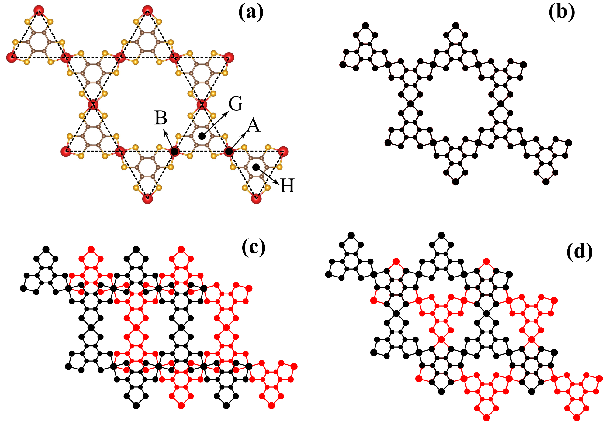
In a previous study [26], we have found the 2ML-AA configuration to be the most stable. There, the calculations were performed using the non-local vdW-DF2 [38] correction to describe the vdW interactions. Indeed, the energetic preference of 2ML-AA was also verified in Refs. [39; 40] using different approaches to describe the long range vdW interactions [41; 42; 43]. In contrast, while Ref. [35] shows an energetic preference for the 2ML-GH configuration using the vdW-D3 [44], our results with this functional corroborates the previous works, showing a preference for the 2ML-AA case.
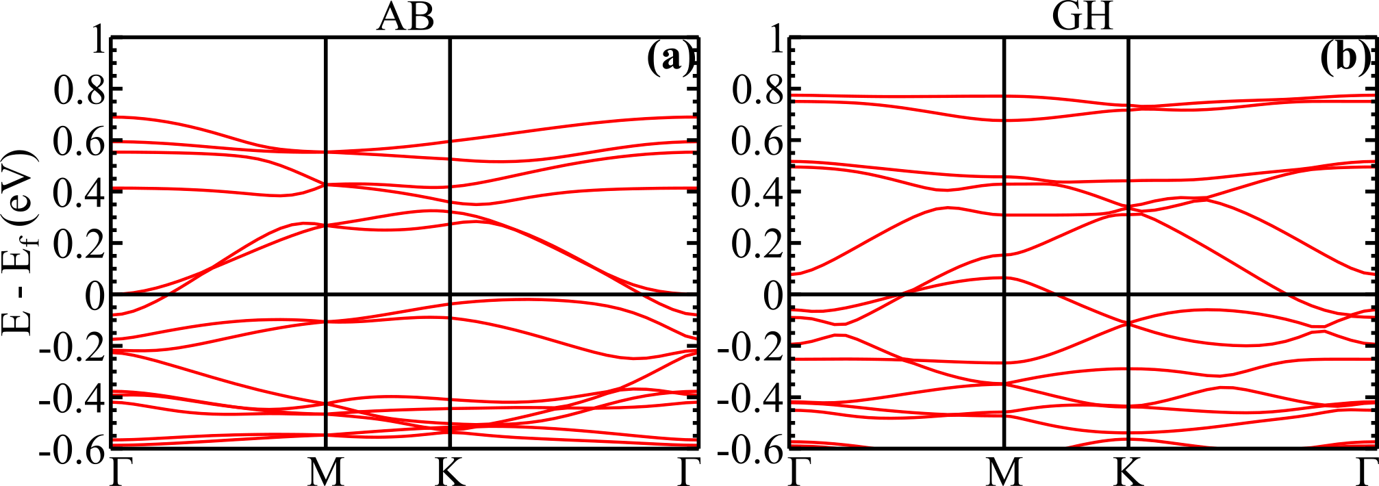
Notice that, despite the weak chemical interactions (essentially vdW) between the stacked layers, the electronic band structure of multilayered (NiC4S systems strongly depends on the stacking geometry. Indeed, the 2ML-AA and -GH configurations present significantly different band structures near the Fermi level, see Appendix A. Moreover, here we are interested in the topological insulator properties of (NiC4S MOFs [25], and such a dependence will reflect on the characteristics of the edge states in bilayer [26], and multilayer (NiC4S.
A detailed analysis of the binding energy 111The binding energy () of (NiC4S bilayer systems is defined as, where and are the total energies of the (NiC4S 2ML-XY, and (free standing) monolayer. Similar definition was applied for the 3ML-XYZ and bulk-XY systems. and geometric properties of different stackings is shown in Table 1. Here, the total energy calculations were performed considering full relaxation of the atomic positions and lattice vectors, until the force in each atom was less than 5 meV/Å. Moreover, we compare results obtained using different functionals, viz.: LDA [46], GGA-PBE [47], local vdW-D3 correction [44], and the non-local vdW-DF2 correction [38]. The wave functions were expanded in a plane-wave basis with cutoff energy of 450 eV. For BZ integration a () k-mesh for bulk (finite stacking) systems was considered. We have also considered the GGA+U method to correct the on-site repulsion of Ni d-orbitals. As shown in Appendix B, these corrections do not affect significantly our results.
| PBE | ||||
|---|---|---|---|---|
| System | ||||
| 1ML | 14.62 | - | 0.00 | 0.000 |
| 2ML-GH | 14.63 | 4.23 | 0.01 | 0.037 |
| 2ML-AB | 14.62 | 3.99 | 0.05 | 0.033 |
| 2ML-AA | 14.62 | 4.69 | 0.01 | 0.022 |
| 3ML-AAA | 14.64 | 3.95 | 0.00 | 0.004 |
| bulk-GH | 14.63 | 3.79 | 0.00 | 0.055 |
| bulk-AB | 14.63 | 3.73 | 0.00 | 0.002 |
| bulk-AA | 14.63 | 3.93 | 0.00 | 0.009 |
| LDA | ||||
| System | ||||
| 1ML | 14.37 | - | 0.00 | 0.000 |
| 2ML-GH | 14.42 | 2.96 | 0.11 | 0.468 |
| 2ML-AB | 14.36 | 3.16 | 0.06 | 0.429 |
| 2ML-AA | 14.44 | 2.96 | 0.08 | 1.051 |
| 3ML-AAA | 14.43 | 3.11 | 0.04 | 1.138 |
| bulk-GH | 14.39 | 3.13 | 0.00 | 0.985 |
| bulk-AB | 14.40 | 3.29 | 0.00 | 0.888 |
| bulk-AA | 14.45 | 3.12 | 0.00 | 1.800 |
| vdW-D3 | ||||
| System | ||||
| 1ML | 14.62 | - | 0.00 | 0.000 |
| 2ML-GH | 14.61 | 3.26 | 0.11 | 0.679 |
| 2ML-AB | 14.60 | 3.34 | 0.15 | 0.661 |
| 2ML-AA | 14.64 | 3.54 | 0.01 | 0.860 |
| 3ML-AAA | 14.64 | 3.57 | 0.00 | 1.206 |
| bulk-GH | 14.62 | 3.31 | 0.00 | 1.501 |
| bulk-AB | 14.60 | 3.46 | 0.00 | 1.404 |
| bulk-AA | 14.65 | 3.35 | 0.00 | 1.968 |
| vdW-DF2 | ||||
| System | ||||
| 1ML | 14.83 | - | 0.00 | 0.000 |
| 2ML-GH | 14.83 | 3.33 | 0.11 | 0.645 |
| 2ML-AB | 14.82 | 3.34 | 0.21 | 0.602 |
| 2ML-AA | 14.86 | 3.64 | 0.01 | 0.803 |
| 3ML-AAA | 14.85 | 3.65 | 0.00 | 1.107 |
| bulk-GH | 14.84 | 3.46 | 0.00 | 1.360 |
| bulk-AB | 14.82 | 3.56 | 0.00 | 1.267 |
| bulk-AA | 14.87 | 3.56 | 0.00 | 1.744 |
Starting with the 2ML case, the PBE results show larger interlayer distances , and lower values of binding energies when compared with the other functionals, thus indicating that the vdW interactions play an important role on the energetic stability and the equilibrium geometry of the multilayered (NiC4S systems. When vdW corrections are included, we find that 2ML-AA stackings are more stable than 2ML-GH 222Although our calculations have more base functions and denser k-grid than that of Ref. [35], we have also run calculations with exact the same parameters listed in this reference, but even in this case we find that the 2ML-AA stacking is more stable., with a difference of 0.15 eV/layer. The 2ML-AA stacking shows 0.80 (0.86) eV/layer, and interlayer distance 3.64 (3.54) Å, within the vdW-DF2 (vdW-D3) functional. In general, the bond distances obtained from the vdW-DF2 approach are larger than those obtained by the vdW-D3 approximation. Nonetheless, both vdW corrections capture the enhancement of the vertical corrugation () due to the reduction of the interlayer distance in 2ML-AB, =0.10.21 and 0.10.15 Å, for vdW-DF2 and -D3, respectively. The energetic preference for the 2ML-AA configurations has been also verified within the LDA approximation. However, a comparison between the LDA and vdW results show that, within the LDA approach, the difference between 2ML-AA and -AB stackings is larger (0.62 eV/layer), and the 2ML-AA configuration shows a smaller interlayer distance (2.96 Å), which leads to a larger corrugation =0.08 Å.
For trilayers and the bulk systems, further binding energy results, shown in Table 1, also indicate the energetic preference for the AA stacking (3ML-AAA and bulk-AA). In comparison with the 2ML-AA case, the binding energy of the bulk-AA system increases by 1 eV/layer, followed by a reduction of the interlayer distance by 0.08 Å, =3.643.56 Å, (0.19 Å, 3.543.35 Å) using the vdW-DF2 (vdW-D3) approximation. Within the LDA approach, we have also found the bulk-AA stacking to be the most stable. However, in contrast with the (vdW) results above, at the equilibrium geometry the interlayer distance increases by 0.16 Å when compared with the bilayer 2ML-AA, 2.963.12 Å. These findings suggest that the vdW and LDA approximations present the same qualitative picture regarding the energetic stability of multilayered (NiC4S systems. However, the LDA approach fails to describe their equilibrium geometries. On the other hand, the PBE functional fail to describe the interlayer interaction, with the interlayer distance overestimated and smaller binding energies. Hereafter we will consider the most stable eclipsed (AA) geometry, obtained using the vdW-DF2 approach.
II.2 Electronic properties
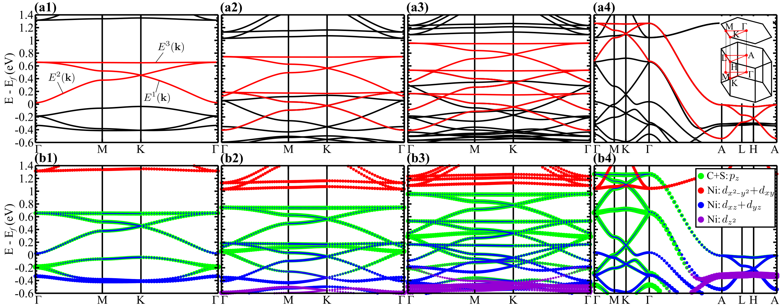
To analyze the electronic structure of the AA stacking, we first consider the DFT results without SOC, as shown in Fig. 2 for 1ML, 2ML, 3ML, and bulk (NiC4S systems. Later on, in Section II.3, we will introduce the SOC to discuss the topological edge states.
For the single layer (NiC4S, the typical kagome bands (KBs), indicated by red lines in Fig. 2(a1), are characterized by two energy bands [ and ] with linear dispersion at the K-point, yielding a Dirac cone, connected to a nearly flat band [] at the -point. The orbital projection, Fig. 2(b1), shows that the KBs are mostly composed by C-pz and S-pz orbitals, while near the center of the Brilloin zone, and along the M-K direction, the Ni-dxz and -dyz orbitals also contribute to the formation of those energy bands. For the 2ML-AA case, one finds two sets of KBs, Fig. 2(a2). There, one set of KBs is fully unoccupied, while the other is partially occupied, with the Dirac point lying slightly below the Fermi level. Such a metallic character is also seen in 3ML, Fig. 2(a3), where three sets of KBs are seen. The orbital projection on these energy bands, Figs. 2(b2) and 2(b3), reveal that, despite showing similar energy dispersion, the KBs present distinct orbital distribution. Namely, the contribution of the Ni-dxz/dyz [blue circles in Fig. 2(b1)-(b3)] orbitals are larger on high energy KBs, whereas the C-pz and S-pz orbitals [green circles in Fig. 2(b1)-(b3)] are dominant on the low energy KBs. Such an orbital distribution has been strengthened in the (NiC4S bulk system. As shown in Figs. 2(a4) and 2(b4), the contribution of the Ni-d (C-pz and S-pz) orbitals becomes dominant on the fully occupied (empty) KBs at high (low) energy, which are localized along the A-L-H-A (-M-K-) directions, see inset of Fig. 2(a4).
II.2.1 Effective tight-binding model
Within the eclipsed AA stacking geometry, the interlayer coupling is mostly given by weak vdW interactions between kagome sites aligned along the stacking direction . Given this scenario, we propose a tight-binding (TB) model, for the stacking of layers, considering first neighbors coupling between monolayers. The resulting Hamiltonian reads
| (1) |
where labels the subspace of each layer , is a identity matrix within this subspace, and is the in-plane momentum. The -layer Hamiltonian above is written in terms of the monolayer’s Hamiltonian , which gives the characteristic KBs dispersion. The vdW interlayer coupling is set by , for which the diagonal form () labels the direct coupling between equivalent atoms in the AA stacking geometry. The second term of is a tridiagonal Toeplitz matrix [49], yielding a closed form for the eigenvalues as
| (2) |
with being the kagome monolayer dispersion [Fig.2(a1)], where labels each of the three KBs for each set . The eigenvectors are , where the first term is an eigenstate of . To understand the second quantum number and the eigenstate component , it is interesting to notice that the tridiagonal Toeplitz form of the coupling is equivalent to the Hamiltonian of a scalar -sites chain, i.e., a quantum well along the stacking direction. Namely, , where is a normalization factor, and
| (3) |
is the contribution of the state to the -th layer. In the second form of above, we use the quantum well analogy to introduce as the quantized momentum along the stacking direction , where is the interlayer distance, and is the effective stacking length 333In this analogy, the quantum well chain has sites distant by , yielding a length . A hard-wall boundary condition makes , such that the real layers lie within .. This analogy is useful to interpret the layer localization and the electric field effects below.
To obtain an estimate for , we compare the first-principles band structures with the eigenvalues of our TB model. The first-principles energy dispersion for 2ML and 3ML, Fig. 2, show that each set of KBs are nearly rigidly shifted from one another. This matches the results of the TB model, where is independent of . For 2ML [Fig. 2(a2)], the two sets ( and 2) of KBs are distant by eV, thus eV. For the 3ML case we also find eV.
Taking the bulk limit of layers, we can explore the quantum well analogy to express , assuming that now is a continuous variable, since . The dispersion is clearly seen in Fig. 2(a4) connecting the topmost and bottommost KBs along the -A direction (). From this dispersion, we obtain eV. Such an increase of (0.28 0.31 eV), although small, is a result of the reduction of the interlayer distance in the bulk system with respect to the few layer systems, 2ML or 3ML in Table 1.
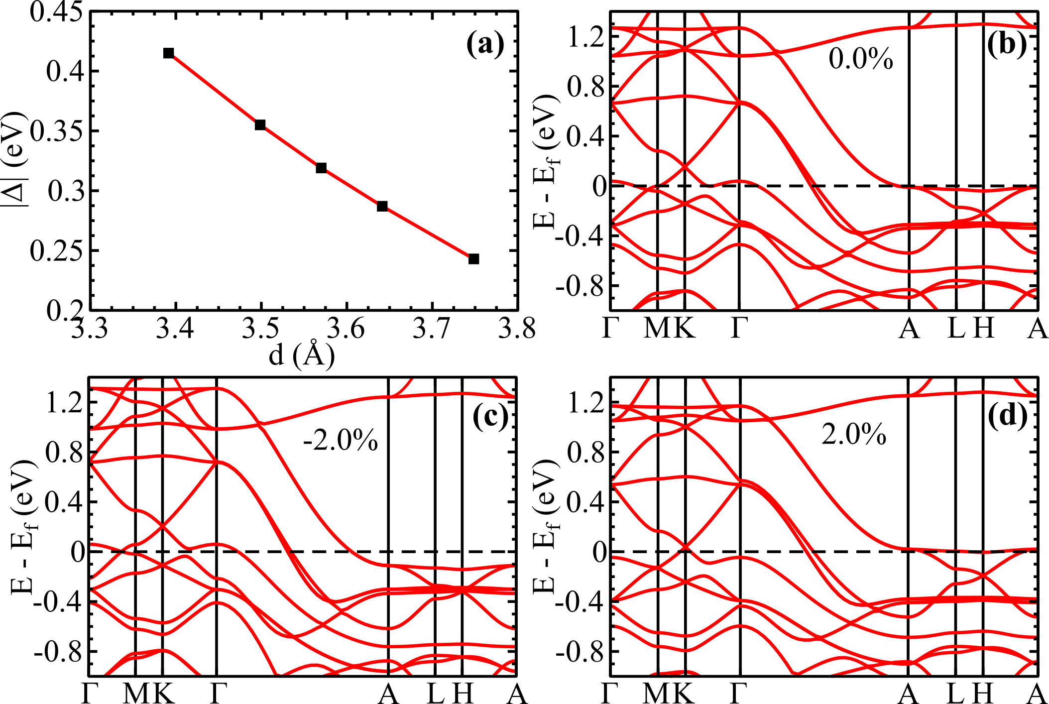
To further explore the band width changes, and support our TB model, in Fig. 3(a) we show as a function of the interlayer spacing for the (NiC4S bulk system. This distance can be controlled by an external pressure (uniaxial strain), thus allowing us to tune . Since the coupling reflects the hybridization of neighboring layers, it decreases as increases. As discussed above, is extracted from the bands connecting KBs along the -A direction. At the equilibrium interlayer distance, =3.56 Å, the energy difference between the upper- and bottommost KBs is about 1.24 eV, Fig. 3(b). Meanwhile, for =3.63 (3.49) Å, this energy split reduces (increases) to 1.12 (1.44) eV [Figs. 3(c) and 3(d)]. That is, a % uniaxial strain induces a % change in .
II.2.2 Layer localization
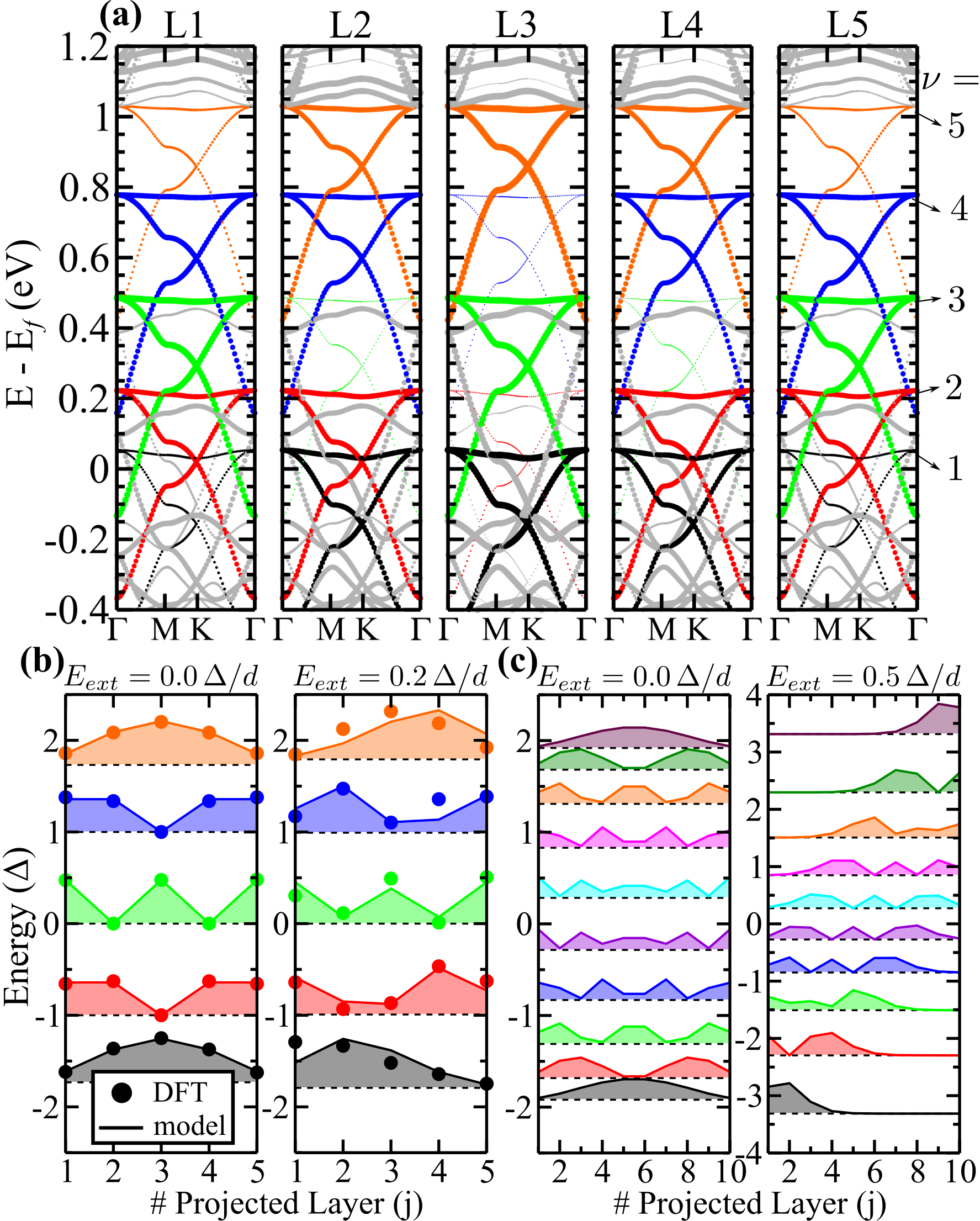
The quantum well analogy, introduced above, enricher our discussion in the layer localization of the kagome states for finite AA stackings. First, in order to verify the validity of this model, we performed first-principles DFT calculations of the KBs for a 5ML slab. Panels L1 to L5 in Fig. 4(a) show the band structures projected on each layer , and indicates the sets of KBs for clarity. Even though the band structure is dense at low energies, it is possible to see that: (i) the highest and the lowest KBs () are mostly localized in the inner layers (L2, L3, L4); (ii) L3 does not contribute to , which localizes mostly on the outer layers; (iii) the KBs contributes mostly to L1, L3 and L5. These features are more clearly seen in the circles of the left panel in Fig. 4(b), which compares the layer projections extracted from the DFT data [Fig. 4(a)], with the TB solutions. Indeed, these projections match remarkably well, thus validating the TB model.
In the presence of an external perpendicular electric field , the projections tend to shift to the outer layers. This is shown in Fig. 4(b) and (c), for a 5ML and 10ML slab respectively. There, we compare the eigenstate distributions among the layers in the absence (left panels) and presence (right panels) of . For a 5ML slab, the DFT data on the right panel of Fig. 4(b) is obtained for a nominal eV/Å. However, due to charge rearrangement between the layers, the actual electric field is inhomogeneous across the layers. Nonetheless, the DFT data matches qualitatively well with the TB model for an effective uniform field eV/Å. Thus, the localization of each state follows the on-site energy shift due to , e.g., the lower energy KBs shifts towards L1.
The same behavior is extrapolated to thicker slabs, for instance a 10ML slab as shown in Fig. 4(c). Therefore allows one to control the layer-localization of the KBs projection. In turn, combining this feature with the tunability of the Fermi energy (e.g., doping), one obtains an interesting engineering of the layer localization of topological edge states, which we discuss in the next section.
II.3 Edge states
The SOC opens an energy gap at the degenerated points ( and K) of each set of KBs, yielding a QSH phase [25; 26]. Interestingly, the weak vdW coupling between the layers of our (NiC4S AA stacking leads to a series of nearly independent edge states in each layer. To model this layered QSH phase, we add the SOC to of our TB model, since the large number of atoms involved in ribbon geometries makes first-principles calculations unattainable. The on-site, hopping, and SOC parameters within the single layer, and the coupling between layers were obtained by fitting the first-principles DFT band structure of the bulk system. Further details can be found in the Appendix C and in Refs. [26; 12].
II.3.1 Edge states on a finite stacking
In this section we consider a 10ML AA stacking in a ribbon geometry. Nevertheless, the following discussion applies to any finite stacking. First, in the absence of electric fields, we calculate the spin-polarized edge states and present its projections into the topmost (L10), middle (L5), and bottommost (L1) layers in Figs. 5(b1)–5(b3). These projections agree with the layer resolved distribution of the KBs discussed previously. For instance, the state (low energy) is mostly located in the middle layer. The same is true for the (high energy) state, since their KBs projections are similar, see left panel of Fig. 4(c). On the other hand, states within are spread along many layers, as illustrated in Fig. 5(a). These results tell us that the vdW coupling between layers reflects into weakly coupled QSH edge states. Such edge states distribution allows for an unexploited control of the edge currents. For instance, tuning the Fermi level to the state, the helical currents will flow mostly through middle of the slab, while for state is distributed along its extremities, see top panel of Fig. 5(a).
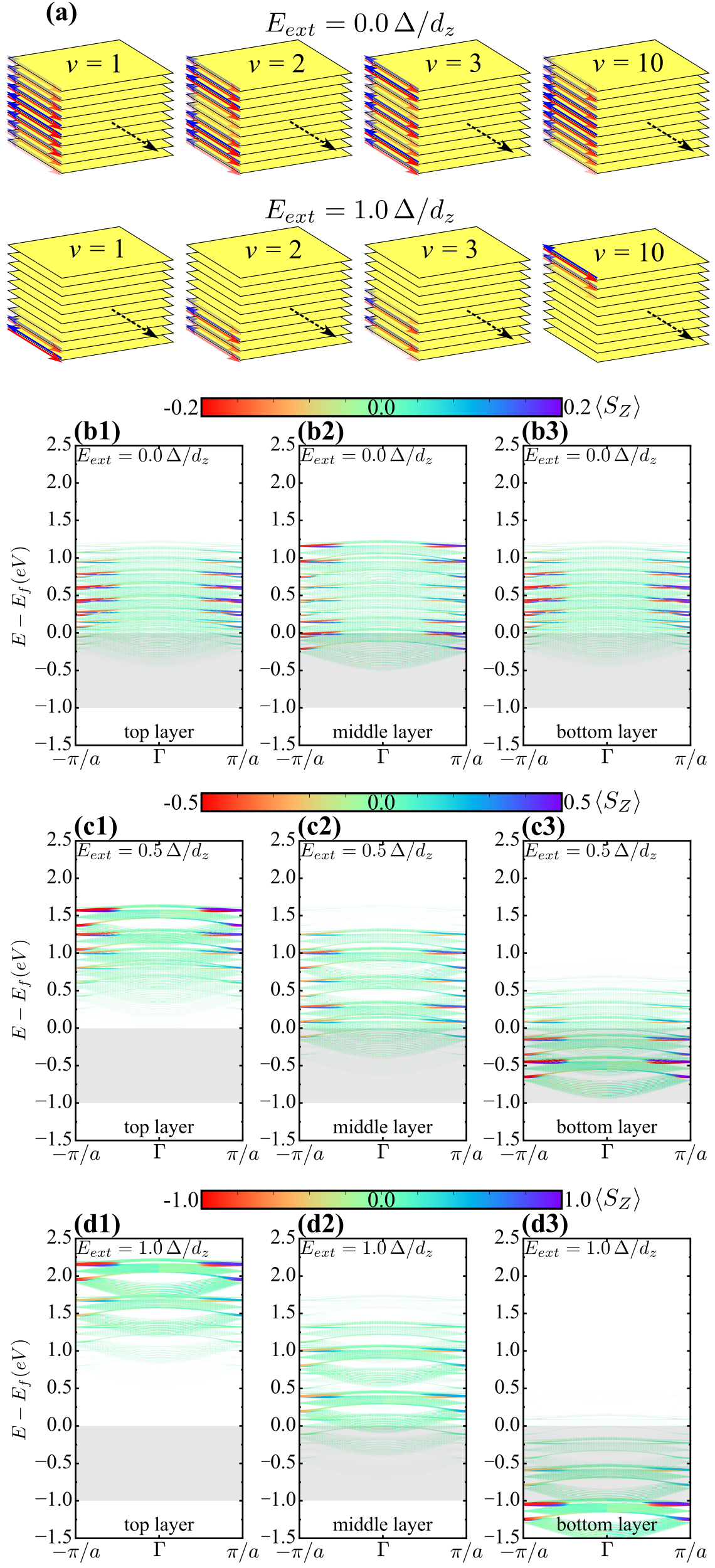
On the other hand, in the presence of , the layer localization of the edge states follows that of the KBs, see right panel of Fig. 4(c). This allows for a fine tuning of the edge states contributions near the Fermi level. To illustrate, Figs. 5(c1)-(c3) show the edge state dispersions for an external field eV/Å. Here, we can see the lower (higher) energy edge states beginning to localize in the bottom (top) layer. Increasing the external field, , the localization effect is enhanced, compare Figs, 5(c3) and (d3). That is, the field changes the on-site energies of each layer, pushing the state towards the bottom layer, as depicted in Fig. 5(a). Consequently, the states near the Fermi level [shaded area in Figs. 5(b)-(d).] are mostly located in the bottom layer. If the field is reversed, , the states near the Fermi level will switch the localization to the top layer. This tuning of the edge states, by and/or changing the Fermi level, allow for an additional degree of freedom that can be useful to design electronic (layertronic) devices based on topologically protected edge currents in metal organic frameworks.
II.3.2 Edge states on the bulk stacking
The electronic confinement effects, present in the few layers systems, no longer takes place in the bulk phase. Here, the weakly coupled edge states from each layer are evenly spread along the side surfaces of the bulk staking, as shown schematically in Fig. 6(a1). Nonetheless, these side surface states carry the characteristics of the individual QSH edge states of the monolayers.
As discussed previously, the infinite superposition of the KBs gives rise to an continuum energy dispersion , where is the wave vector parallel to the stacking direction -A. This bulk dispersion is projected in the 2D BZ of the side surface [Fig. 6(a2) and 6(b)], yielding a continuum of linear crossings at the edge of the Brillouin zone (X–M ), as shown in Fig. 6(c).
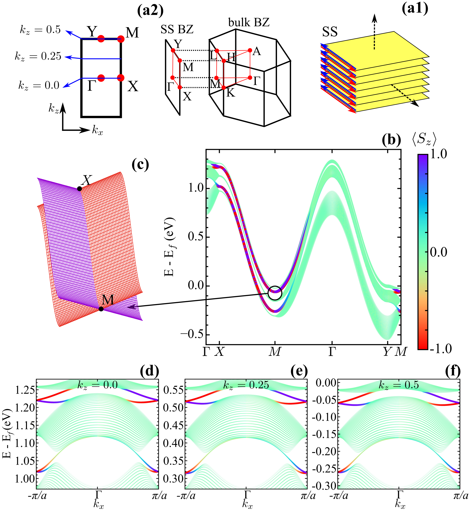
Interestingly, this peculiar V-gutter-like edge state dispersion [Fig. 6(c)] is highly anisotropic. An effective model for these states can be cast as a individual 2DTI edge states coupled along the stacking direction, wich reads
| (4) |
where is the identity matrix, is third Pauli matrix in spin space, is the velocity of the edge states along , and is the same interlayer coupling from the bulk model. Along , the states are helical with constant velocities for spin up and down, while along the velocity is spin independent, but changes with or Fermi energy, . This anisotropy is a consequence of the weak vdW coupling between the stacked layers. Thus, as shown in Fig. 3, the dynamics along can be further controlled by changing with the uniaxial strain.
III Conclusion
In this paper, we show that electronic layer localization can be engineered in multilayer MOFs by controlling the Fermi level (e.g., doping) and an external electric field . This is possible due to the van der Waals (vdW) coupling between adjacent layers on eclipsed AA stackings. Here, we consider the (NiC4S MOFs, showing that AA stacking is the most stable for this material. Nonetheless, our results remain valid for other MOFs that also allow for eclipsed stackings. The interlayer vdW coupling reflects into weakly coupled topological edge states in each monolayer of the stackings. Consequently, we have shown that the layer localization of edge states can be controlled by , applied along the stacking direction, thus providing a novel degree of freedom to the design of TI based electronics.
Furthermore, extrapolating the system to an infinite stacking of nanoribbons, the weak vdW coupling between layers leads to a new V-gutter-like Dirac states in the side surfaces. This new surface states are highly anisotropic, showing a trivial velocity along the stacking direction, while along the monolayer edge a helical topological current is always present for a wide range of energy.
IV ACKNOWLEDGMENTS
The authors acknowledge financial support from the Brazilian agencies CNPq, and FAPEMIG, and the CENAPAD-SP and Laboratório Nacional de Computação Científica (LNCC-SCAFMat) for computer time.
Appendix A Band structure for bilayer stacking
For the (NiC4S bilayer, the stacking order has great impact in the electronic properties. For instance, in the mirror symmetric AA stacking, Fig. 2(a2), we find sets of the characteristc kagome band dispersion. On the other hand, for the non-mirror symmetric stacking, Fig. 7(a) and (b), the coupling between the layers leads to a different hybridization between the states, where the characteristic kagome bands are no longer present.
Appendix B DFT+U
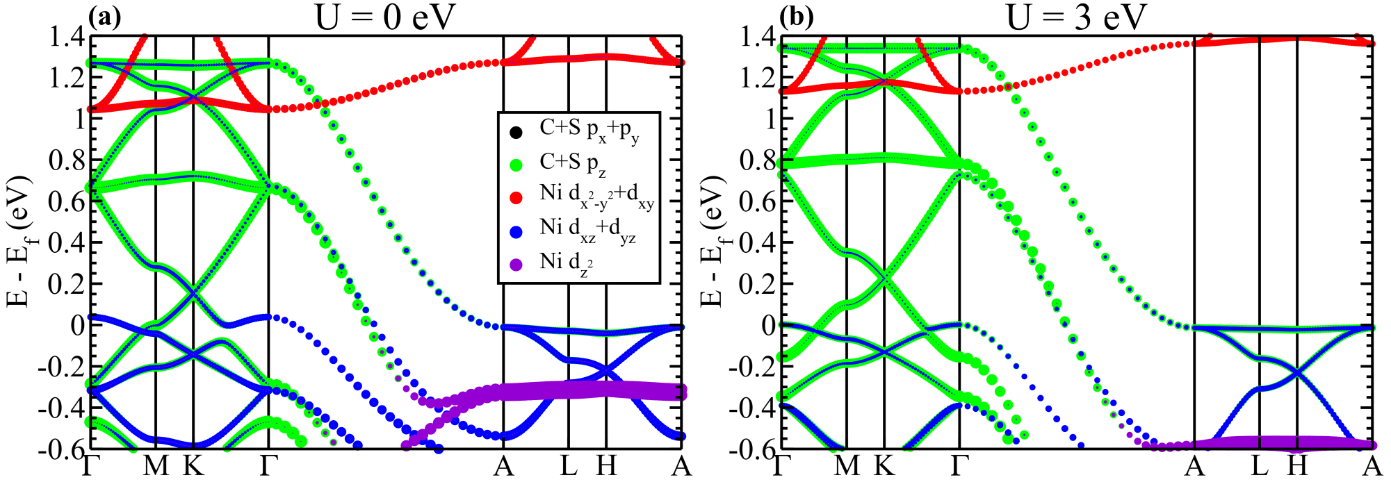
We have performed GGA+U calculations [51] in order to verify the effects of the Hubbard on-site repulsion term for the d-orbitals of Ni in (NiC4S. We find that our main results are not affected by this correction. The comparison between the eV and eV cases in Fig. 8(a) and (b) shows that the Ni d orbitals goes slightly down in energy for a finite , which gives a negligible change in the charge state of Ni atoms, going from for to for eV. Nevertheless, Fig. 8 shows that the Kagome band dispersions are not significantly affected by . Since this is the main characteristic that leads to the tunability of the layer contributions (the sets of kagome bands), we can conclude that our results are robust, and the Hubbard repulsion term can be neglected here.
Appendix C TB model parameters from DFT
The considered tight-binding (TB) Hamiltonian is given by
| (5) |
where contains the on-site energy and hoppings within each layer ,
| (6) |
with and indicating sites in the same layer, and sum over runs over all layers. is the intrinsic spin-orbit coupling,
| (7) |
The last term, contains the coupling between layers,
| (8) |
where and indicates the same site, but in different layers. Here, , , () is the creation (annihilation) operators of an electron in the -th site with spin , and are the spin Pauli matrices. The vectors connect the -th to the -th site. For the hoppings ( and ) and spin-orbit couplings (), we consider a distance dependent parametrization, which allow us to control the hopping range. This parametrization reads
| (9) |
| (10) |
and
| (11) |
All hoppings are normalized in relation to the first neighbor hopping, by the factor and , where is the interlayer distance. In Fig. 9 we show a comparison between the DFT and TB model, using the parameters shown in Tab. 2. Note that the TB parameter is consistent with the one obtained through the analytic model.
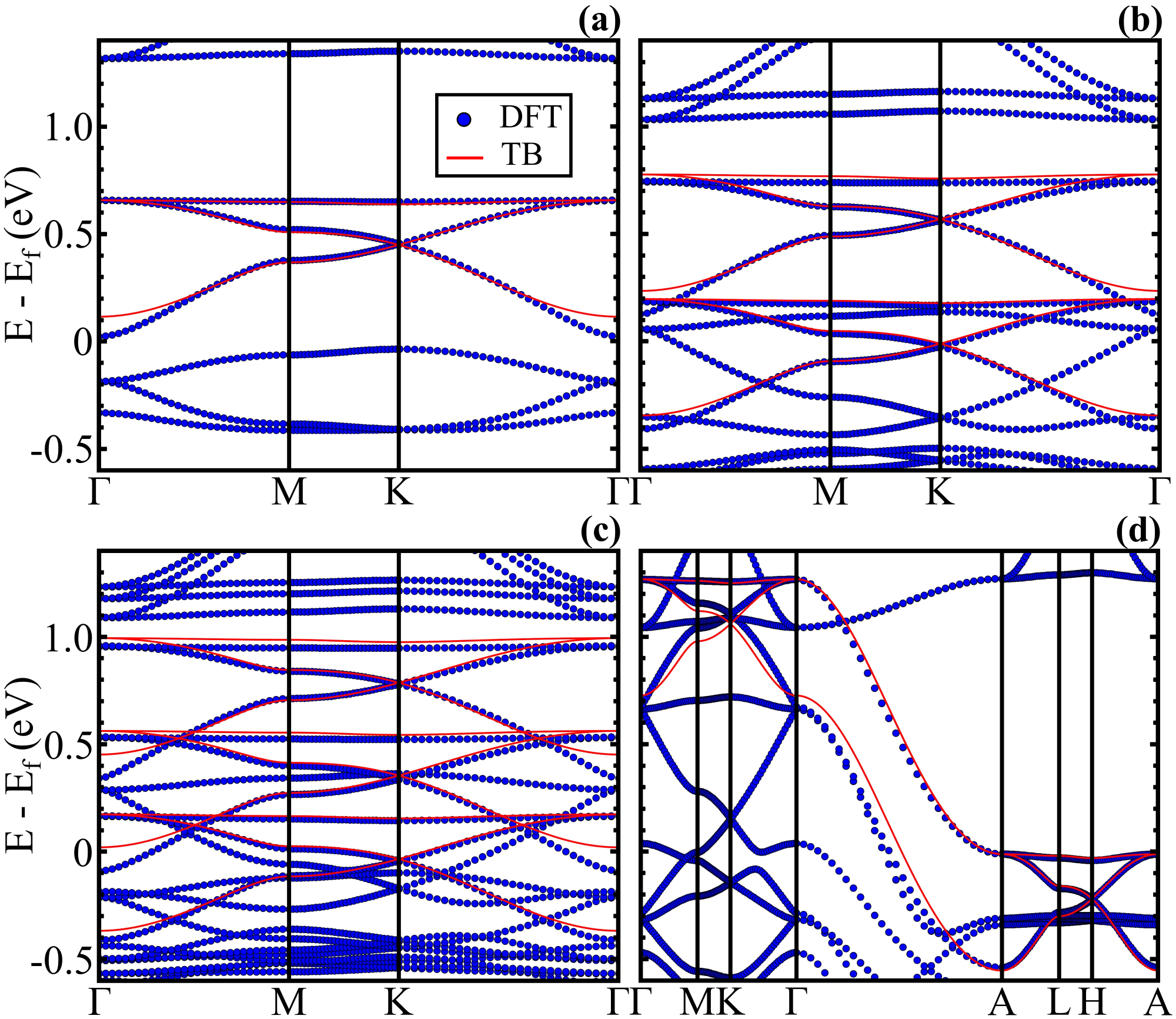
| System | = | ||||
|---|---|---|---|---|---|
| 1L | 0.50 | -0.08 | 3.0 | 0.0 | - |
| 2L | 0.33 | -0.08 | 3.0 | 0.0 | -0.29 |
| 3L | 0.42 | -0.08 | 3.0 | 0.0 | -0.29 |
| bulk | 0.44 | -0.08 | 3.0 | 0.0 | -0.32 |
References
- Sinova et al. [2015] J. Sinova, S. O. Valenzuela, J. Wunderlich, C. H. Back, and T. Jungwirth, “Spin hall effects,” Rev. Mod. Phys. 87, 1213–1260 (2015).
- Kou et al. [2017] L. Kou, Y. Ma, Z. Sun, T. Heine, and C. Chen, “Two-dimensional topological insulators: Progress and prospects,” The Journal of Physical Chemistry Letters 8, 1905–1919 (2017).
- Kane and Mele [2005] C. L. Kane and E. J. Mele, “Quantum spin hall effect in graphene,” Phys. Rev. Lett. 95, 226801 (2005).
- Yao et al. [2007] Y. Yao, F. Ye, X.-L. Qi, S.-C. Zhang, and Z. Fang, “Spin-orbit gap of graphene: First-principles calculations,” Phys. Rev. B 75, 041401 (2007).
- Rodríguez-San-Miguel, Amo-Ochoa, and Zamora [2016] D. Rodríguez-San-Miguel, P. Amo-Ochoa, and F. Zamora, “Masterchem: cooking 2d-polymers,” Chem. Commun. 52, 4113–4127 (2016).
- Colson and Dichtel [2013] J. W. Colson and W. R. Dichtel, “Rationally synthesized two-dimensional polymers,” Nature Chemistry 5, 453 (2013).
- Chen, Dai, and Zeng [2015] S. Chen, J. Dai, and X. C. Zeng, “Metal–organic kagome lattices m3(2,3,6,7,10,11-hexaiminotriphenylene)2 (m = ni and cu): from semiconducting to metallic by metal substitution,” Phys. Chem. Chem. Phys. 17, 5954–5958 (2015).
- Maeda, Sakamoto, and Nishihara [2016] H. Maeda, R. Sakamoto, and H. Nishihara, “Coordination programming of two-dimensional metal complex frameworks,” Langmuir 32, 2527–2538 (2016).
- Zhao et al. [2018] W. Zhao, J. Peng, W. Wang, S. Liu, Q. Zhao, and W. Huang, “Ultrathin two-dimensional metal-organic framework nanosheets for functional electronic devices,” Coordination Chemistry Reviews 377, 44 – 63 (2018).
- Gutzler [2016] R. Gutzler, “Band-structure engineering in conjugated 2d polymers,” Phys. Chem. Chem. Phys. 18, 29092–29100 (2016).
- Chakravarty, Mandal, and Sarkar [2016] C. Chakravarty, B. Mandal, and P. Sarkar, “Bis(dithioline)-based metal–organic frameworks with superior electronic and magnetic properties: Spin frustration to spintronics and gas sensing,” The Journal of Physical Chemistry C 120, 28307–28319 (2016).
- Crasto de Lima, Ferreira, and Miwa [2018] F. Crasto de Lima, G. J. Ferreira, and R. H. Miwa, “Quantum anomalous hall effect in metal-bis(dithiolene), magnetic properties, doping and interfacing graphene,” Phys. Chem. Chem. Phys. 20, 22652–22659 (2018).
- Dong et al. [2018] R. Dong, Z. Zhang, D. C. Tranca, S. Zhou, M. Wang, P. Adler, Z. Liao, F. Liu, Y. Sun, W. Shi, Z. Zhang, E. Zschech, S. C. B. Mannsfeld, C. Felser, and X. Feng, “A coronene-based semiconducting two-dimensional metal-organic framework with ferromagnetic behavior,” Nature Communications 9, 2637 (2018).
- Liu et al. [2013] Z. Liu, Z.-F. Wang, J.-W. Mei, Y.-S. Wu, and F. Liu, “Flat chern band in a two-dimensional organometallic framework,” Phys. Rev. Lett. 110, 106804 (2013).
- Zhao et al. [2014] B. Zhao, J. Zhang, W. Feng, Y. Yao, and Z. Yang, “Quantum spin hall and metallic states in an organic material,” Phys. Rev. B 90, 201403 (2014).
- Zhou et al. [2015] Q. Zhou, J. Wang, T. S. Chwee, G. Wu, X. Wang, Q. Ye, J. Xu, and S.-W. Yang, “Topological insulators based on 2d shape-persistent organic ligand complexes,” Nanoscale 7, 727–735 (2015).
- Zhang et al. [2016a] L. Z. Zhang, Z. F. Wang, B. Huang, B. Cui, Z. Wang, S. X. Du, H.-J. Gao, and F. Liu, “Intrinsic two-dimensional organic topological insulators in metal–dicyanoanthracene lattices,” Nano Letters 16, 2072–2075 (2016a).
- Yamada et al. [2016] M. G. Yamada, T. Soejima, N. Tsuji, D. Hirai, M. Dincă, and H. Aoki, “First-principles design of a half-filled flat band of the kagome lattice in two-dimensional metal-organic frameworks,” Phys. Rev. B 94, 081102 (2016).
- Zhang et al. [2016b] X. Zhang, Z. Wang, M. Zhao, and F. Liu, “Tunable topological states in electron-doped htt-pt,” Phys. Rev. B 93, 165401 (2016b).
- Hsu et al. [2018] C.-H. Hsu, Z.-Q. Huang, G. M. Macam, F.-C. Chuang, and L. Huang, “Prediction of two-dimensional organic topological insulator in metal-dcb lattices,” Applied Physics Letters 113, 233301 (2018).
- Ni et al. [2018] X. Ni, W. Jiang, H. Huang, K.-H. Jin, and F. Liu, “Intrinsic quantum anomalous hall effect in a two-dimensional anilato-based lattice,” Nanoscale 10, 11901–11906 (2018).
- Sun et al. [2018] H. Sun, S. Tan, M. Feng, J. Zhao, and H. Petek, “Deconstruction of the electronic properties of a topological insulator with a two-dimensional noble metal–organic honeycomb–kagome band structure,” The Journal of Physical Chemistry C 122, 18659–18668 (2018).
- Kambe et al. [2013] T. Kambe, R. Sakamoto, K. Hoshiko, K. Takada, M. Miyachi, J.-H. Ryu, S. Sasaki, J. Kim, K. Nakazato, M. Takata, and H. Nishihara, “-conjugated nickel bis(dithiolene) complex nanosheet,” Journal of the American Chemical Society 135, 2462–2465 (2013).
- Pal et al. [2015] T. Pal, T. Kambe, T. Kusamoto, M. L. Foo, R. Matsuoka, R. Sakamoto, and H. Nishihara, “Interfacial synthesis of electrically conducting palladium bis(dithiolene) complex nanosheet,” ChemPlusChem 80, 1255–1258 (2015).
- Wang, Su, and Liu [2013] Z. F. Wang, N. Su, and F. Liu, “Prediction of a two-dimensional organic topological insulator,” Nano Letters 13, 2842–2845 (2013), pMID: 23678979.
- de Lima, Ferreira, and Miwa [2017] F. C. de Lima, G. J. Ferreira, and R. H. Miwa, “Tuning the topological states in metal-organic bilayers,” Phys. Rev. B 96, 115426 (2017).
- Wolf et al. [2001] S. A. Wolf, D. D. Awschalom, R. A. Buhrman, J. M. Daughton, S. von Molnár, M. L. Roukes, A. Y. Chtchelkanova, and D. M. Treger, “Spintronics: A spin-based electronics vision for the future,” Science 294, 1488–1495 (2001).
- Schaibley et al. [2016] J. R. Schaibley, H. Yu, G. Clark, P. Rivera, J. S. Ross, K. L. Seyler, W. Yao, and X. Xu, “Valleytronics in 2d materials,” Nature Reviews Materials 1, 16055 (2016).
- Huang et al. [2017] B. Huang, K.-H. Jin, B. Cui, F. Zhai, J. Mei, and F. Liu, “Bending strain engineering in quantum spin hall system for controlling spin currents,” Nature Communications 8, 15850 (2017).
- Jaskólski et al. [2018] W. Jaskólski, M. Pelc, G. W. Bryant, L. Chico, and A. Ayuela, “Controlling the layer localization of gapless states in bilayer graphene with a gate voltage,” 2D Materials 5, 025006 (2018).
- Geim and Grigorieva [2013] A. K. Geim and I. V. Grigorieva, “Van der waals heterostructures,” Nature 499, 419 (2013).
- Novoselov et al. [2016] K. S. Novoselov, A. Mishchenko, A. Carvalho, and A. H. Castro Neto, “2d materials and van der waals heterostructures,” Science 353 (2016).
- Kim et al. [2011] K. Kim, Z. Lee, B. D. Malone, K. T. Chan, B. Alemán, W. Regan, W. Gannett, M. F. Crommie, M. L. Cohen, and A. Zettl, “Multiply folded graphene,” Phys. Rev. B 83, 245433 (2011).
- Araújo, Ferreira, and Schmidt [2018] A. L. Araújo, G. J. Ferreira, and T. M. Schmidt, “Suppressed topological phase transitions due to nonsymmorphism in snte stacking,” Scientific Reports 8, 9452 (2018).
- Li et al. [2018] S. Li, T.-Y. Lü, J.-C. Zheng, S.-W. Yang, J.-S. Wang, and G. Wu, “Origin of metallicity in 2d multilayer nickel bis(dithiolene) sheets,” 2D Materials 5, 035027 (2018).
- Guo et al. [2019] L. Guo, X. Gu, X. Zhu, and X. Sun, “Recent advances in molecular spintronics: Multifunctional spintronic devices,” Advanced Materials 0, 1805355 (2019).
- Soumyanarayanan et al. [2016] A. Soumyanarayanan, N. Reyren, A. Fert, and C. Panagopoulos, “Emergent phenomena induced by spin-orbit coupling at surfaces and interfaces,” Nature 539, 509 (2016).
- Lee et al. [2010] K. Lee, E. D. Murray, L. Kong, B. I. Lundqvist, and D. C. Langreth, “Higher-accuracy van der waals density functional,” Phys. Rev. B 82, 081101 (2010).
- Shojaei and Kang [2014] F. Shojaei and H. S. Kang, “Continuous tuning of band gap for -conjugated ni bis(dithiolene) complex bilayer,” The Journal of Physical Chemistry C 118, 25626–25632 (2014).
- Silveira, Érika N Lima, and Chacham [2017] O. J. Silveira, Érika N Lima, and H. Chacham, “Bilayers of ni 3 c 12 s 12 and pt 3 c 12 s 12 : graphene-like 2d topological insulators tunable by electric fields,” Journal of Physics: Condensed Matter 29, 465502 (2017).
- Grimme [2006] S. Grimme, “Semiempirical gga-type density functional constructed with a long-range dispersion correction,” Journal of Computational Chemistry 27, 1787–1799 (2006).
- Dion et al. [2004] M. Dion, H. Rydberg, E. Schröder, D. C. Langreth, and B. I. Lundqvist, “Van der waals density functional for general geometries,” Phys. Rev. Lett. 92, 246401 (2004).
- Klimeš, Bowler, and Michaelides [2009] J. Klimeš, D. R. Bowler, and A. Michaelides, “Chemical accuracy for the van der waals density functional,” Journal of Physics: Condensed Matter 22, 022201 (2009).
- Grimme et al. [2010] S. Grimme, J. Antony, S. Ehrlich, and H. Krieg, “A consistent and accurate ab initio parametrization of density functional dispersion correction (dft-d) for the 94 elements h-pu,” The Journal of Chemical Physics 132, 154104 (2010).
- Note [1] The binding energy () of (NiC4S bilayer systems is defined as, where and are the total energies of the (NiC4S 2ML-XY, and (free standing) monolayer. Similar definition was applied for the 3ML-XYZ and bulk-XY systems.
- Perdew and Zunger [1981] J. P. Perdew and A. Zunger, “Self-interaction correction to density-functional approximations for many-electron systems,” Phys. Rev. B 23, 5048–5079 (1981).
- Perdew, Burke, and Ernzerhof [1996] J. P. Perdew, K. Burke, and M. Ernzerhof, “Generalized gradient approximation made simple,” Phys. Rev. Lett. 77, 3865–3868 (1996).
- Note [2] Although our calculations have more base functions and denser k-grid than that of Ref. [35], we have also run calculations with exact the same parameters listed in this reference, but even in this case we find that the 2ML-AA stacking is more stable.
- [49] S. Noschese, L. Pasquini, and L. Reichel, “Tridiagonal toeplitz matrices: properties and novel applications,” Numerical Linear Algebra with Applications 20, 302–326.
- Note [3] In this analogy, the quantum well chain has sites distant by , yielding a length . A hard-wall boundary condition makes , such that the real layers lie within .
- Dudarev et al. [1998] S. L. Dudarev, G. A. Botton, S. Y. Savrasov, C. J. Humphreys, and A. P. Sutton, “Electron-energy-loss spectra and the structural stability of nickel oxide: An lsda+u study,” Phys. Rev. B 57, 1505–1509 (1998).