Proximity-induced superconducting gap in the quantum spin Hall edge state of monolayer WTe2
The quantum spin Hall (QSH) state was recently demonstrated in monolayers of the transition metal dichalcogenide 1T’-WTe2 and is characterized by a band gap in the two-dimensional (2D) interior and helical one-dimensional (1D) edge states Crommie2017 ; Fei2017 ; Wu2018 . Inducing superconductivity in the helical edge states would result in a 1D topological superconductor, a highly sought-after state of matter Alicea2012 . In the present study, we use a novel dry-transfer flip technique to place atomically-thin layers of WTe2 on a van der Waals superconductor, NbSe2. Using scanning tunneling microscopy and spectroscopy (STM/STS), we demonstrate atomically clean surfaces and interfaces and the presence of a proximity-induced superconducting gap in the WTe2 for thicknesses from a monolayer up to 7 crystalline layers. At the edge of the WTe2 monolayer, we show that the superconducting gap coexists with the characteristic spectroscopic signature of the QSH edge state. Taken together, these observations provide conclusive evidence for proximity-induced superconductivity in the QSH edge state in WTe2, a crucial step towards realizing 1D topological superconductivity and Majorana bound states in this van der Waals material platform.
Contemporary interest in topological superconductors has been driven by potential applications of their gapless boundary excitations, which are thought to be emergent Majorana quasiparticles with non-abelian statistics Kitaev2001 ; Fu2008 ; Sarma2015 ; Sato2017 . One path toward topological superconductivity is to realize an intrinsic spinless -wave superconductor Maeno2012 . A powerful alternative is by using a conventional -wave superconductor to induce Cooper pairing in topologically non-trivial states via the superconducting proximity effect, resulting in an effective -wave pairing Fu2009 . This approach has recently been employed to engineer 2D topological superconductivity in epitaxial three-dimensional topological insulator films grown on a superconducting substrate Wang2012 ; Sun2016 , and 1D topological superconductivity by proximitizing a 2D QSH system in buried epitaxial semiconductor quantum wells Hart2014 ; Bocquillon2016 . While such demonstrations mark important milestones, there are clear advantages for exploring topological superconductivity in the van der Waals material platform. Using layered 2D materials allows the 2D QSH edge to be proximitized in vertical heterostructures, circumventing the length restrictions of lateral proximity-effect geometries. Furthermore, the surfaces and edges are readily available for surface probes, allowing detection and fundamental study of signatures of the topological superconducting state. Following recent theoretical predictions Qian2014 , an intrinsic QSH state was demonstrated in a monolayer (ML) of 1T’-WTe2 Crommie2017 ; Fei2017 ; Jia2017 ; Peng2017 ; Wu2018 ; Shi2019 . WTe2 is attractive for studying the QSH edge modes because it can be readily incorporated in van der Waals heterostructures and has shown quantized edge conductance up to Wu2018 . Furthermore, ML WTe2 was recently also shown to host intrinsic superconducting behavior below when electrostatically gated into the conduction band Fatemi2018 ; Sajadi2018 .
In the present work, we study mechanically-exfoliated single- and few-layers of WTe2 which have been transferred onto the van der Waals -wave superconductor NbSe2. We show that this approach induces a superconducting gap in the WTe2 without the need for electrostatic doping and yields a critical temperature much higher than that of the intrinsic WTe2 superconductivity, an experimental advantage which greatly facilitates studies of the interplay of superconductivity and the QSH edge modes. We employ scanning tunneling microscopy and spectroscopy (STM/STS) to investigate the proximity-induced superconducting gap as a function of temperature, magnetic field, and WTe2 thickness. By spatially resolving the spectroscopic features of the WTe2, we find that the superconducting gap coexists with the QSH signature at the ML WTe2 edge, demonstrating critical steps toward identifying 1D topological superconductivity in a van der Waals material system.
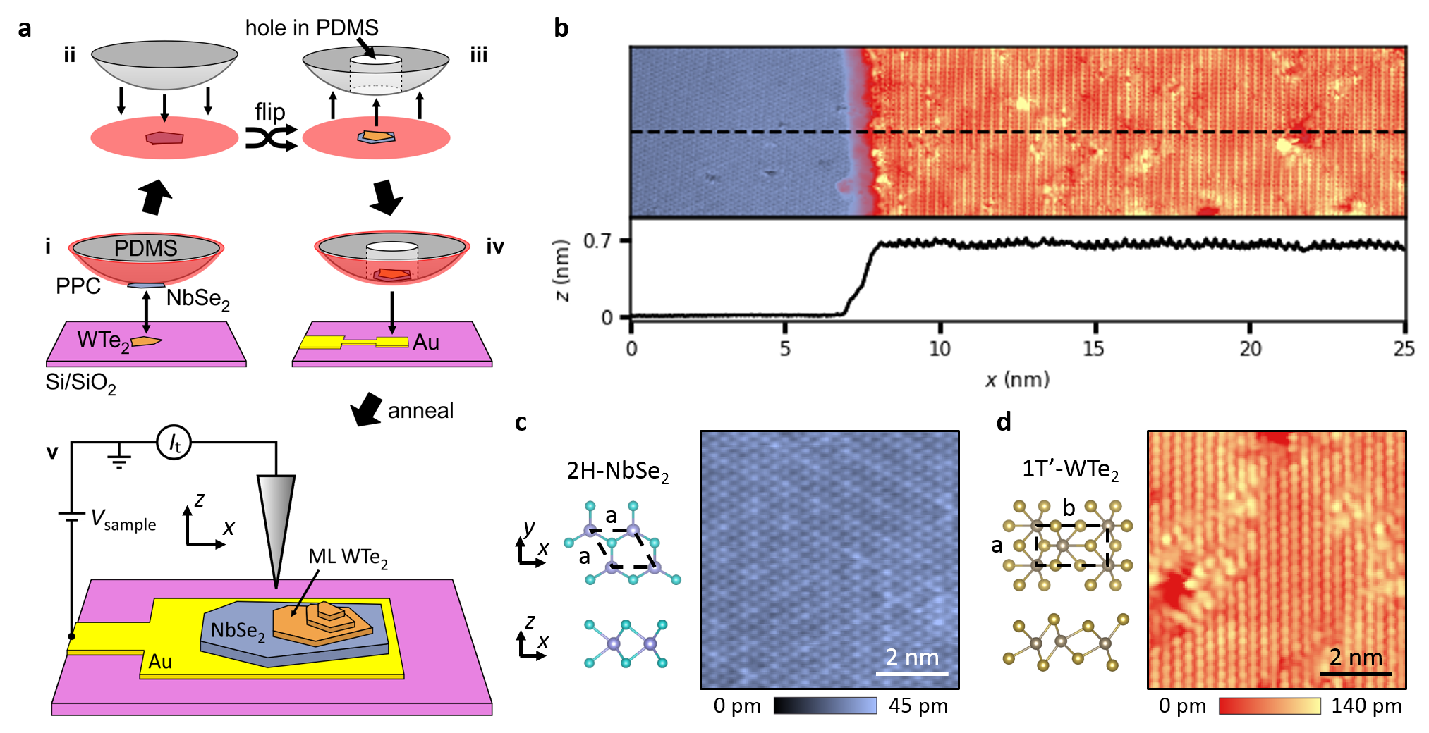
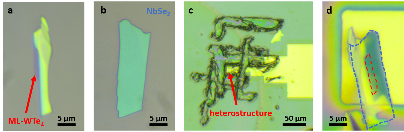
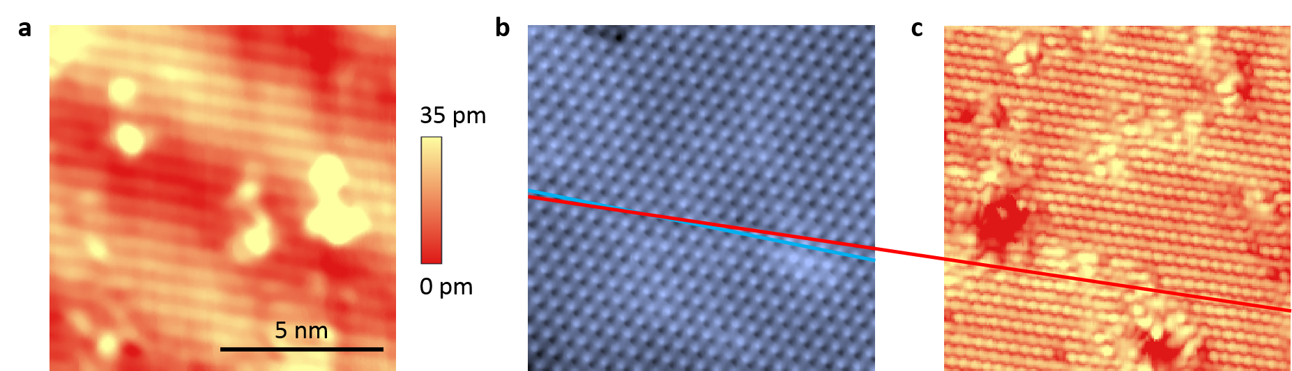
We have developed a novel fabrication technique which enables the assembly and deterministic placement of van der Waals heterostructures in a glove box (Fig. 1a). Though similar methods have been used to fabricate complex encapsulated mesoscale devices Zeng2018 , critically, our technique produces atomically-clean surfaces of air-sensitive materials suitable for high-resolution scanning probe measurements. In detail, WTe2 and NbSe2 are exfoliated from bulk materials and assembled using a PPC/PDMS stamp inside a nitrogen-filled glove box. Subsequently, the PPC film is peeled off, flipped upside down and put onto a second PDMS stamp which has a hole cut into it. This stamp is used to deterministically place the heterostructure onto a pre-patterned gold lead on a SiO2 chip which is mounted and contacted to an STM sample plate. The PPC is then removed by annealing under vacuum conditions and the sample is transferred to the STM, all without intermediate air-exposure and without bringing the heterostructure surface into contact with any polymers or solvents, ensuring the surface cleanliness (for further details see Supplementary Materials). Figure 1b shows an STM image of the resulting heterostructure where the WTe2 ML edge and the underlying NbSe2 are visible, showing atomically-clean surfaces on each material. The profile across the step edge shows a step height of which corresponds to one WTe2 layer Peng2017 , indicating an atomically-clean interface between the WTe2 and NbSe2. In Fig. 1b a weak moiré pattern in the form of diagonal stripes can be seen on the ML WTe2 resulting from the superposition of the two different atomic lattices. The moiré pattern, analyzed in more detail in the Supplementary Materials, corresponds to a twist angle of between the NbSe2 hexagonal unit cell with lattice parameters and WTe2 rectangular unit cell with lattice parameters and (Fig. 1c, d). Atomically-resolved STM images of the NbSe2 surface (Fig. 1c) show the well-known charge density wave Wang2012 , indicating the pristine quality of the NbSe2 flake. Atomically-resolved STM images of the WTe2 (Fig. 1d) are characterized by vertical atomic rows parallel to the -axis of the WTe2 unit cell.
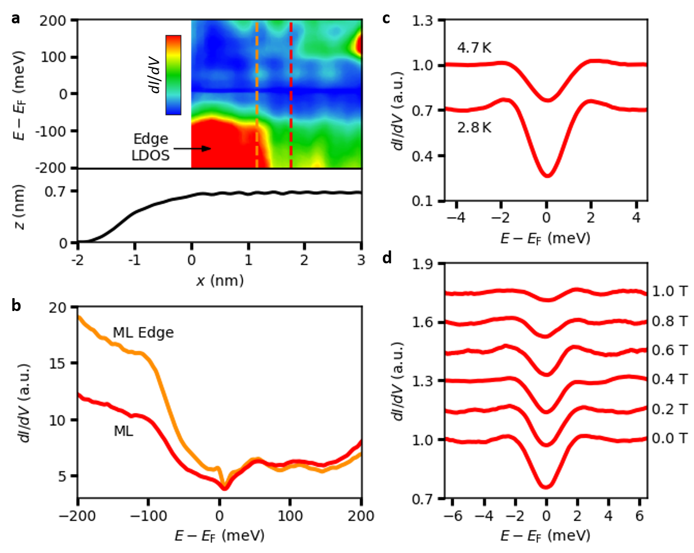
Turning now to spectroscopic analysis of these surfaces, Fig. 2a shows a series of spectra taken along a line perpendicular to the WTe2 ML step edge (upper panel) and the corresponding height profile (lower panel). The spectra clearly show the presence of an increased local density of states (LDOS) near the WTe2 step edge. This feature was recently reported in STM/STS studies of ML films of WTe2 grown on epitaxial graphene substrates Crommie2017 ; Jia2017 . Based on combined evidence from angle-resolved photoemission spectroscopy (ARPES) and STS in Ref. 1, it was concluded that ML WTe2 has a band gap of , and that the increased LDOS at the ML WTe2 edge signifies the metallic QSH edge state. In our monolayer samples, produced via isolation from bulk crystals rather than molecular beam epitaxy, and on superconducting substrates rather than graphene, we observe the same spectroscopic features, which we attribute to the same QSH edge state. Figure 2b shows the averaged spectrum on the WTe2 ML (red) and the ML edge (orange) at the corresponding positions indicated in Fig. 2a. The spectroscopic signature of the QSH edge state is evident primarily in the valence band but, importantly, the edge state also crosses the band gap. Following the interpretation of Ref. 1, the increases in the signal at and correspond to the onset of the WTe2 valence and conduction band, respectively, locating in the ML WTe2 band gap. A non-zero signal in the band gap away from the step edge was proposed to be due to defect states and substrate effects Crommie2017 . In addition, tip-induced band bending may play a role in introducing spectral weight in the WTe2 band gap (see Supplementary Materials). By comparing the positions of the observed spectral features to epitaxially-grown WTe2 on graphene Crommie2017 ; Jia2017 and exfoliated WTe2 Cucchi2018 , we conclude that there is no significant charge transfer from the NbSe2 to the WTe2. This observation is further supported by our density functional theory (DFT) calculations of the ML WTe2/NbSe2 heterostructure, which show only minimal modifications of the WTe2 electronic structure compared to a freestanding WTe2 ML (see Supplementary Materials).
Measurements of the ML WTe2 spectrum over a smaller voltage range (Fig. 2c), reveal a new feature: a superconducting gap-like feature characterized by a dip in the signal at the Fermi energy, with peaks on either side of the gap. Comparison of measurements at and show that the gap deepens and the peaks sharpen at lower temperature. The evolution of the superconducting gap-like feature under application of a surface-normal magnetic field at (Fig. 2d) shows that with increasing magnetic field, the gap becomes less deep and the peaks flatten out until the gap features have nearly vanished at . We find that a fit of the Bardeen-–Cooper-–Schrieffer (BCS) model describes both the monolayer WTe2 and the NbSe2 data well (Fig. 3a). For NbSe2, the fit results in a superconducting gap of , while for the WTe2 we find . In addition to following the trend of a superconducting gap with applied magnetic field, the vanishing of the gap near is similar to the Ginzburg–-Landau estimate for the upper critical field of bulk NbSe2 Garoche1976 . We conclude that the gap feature observed on the ML WTe2 is indeed a superconducting gap.
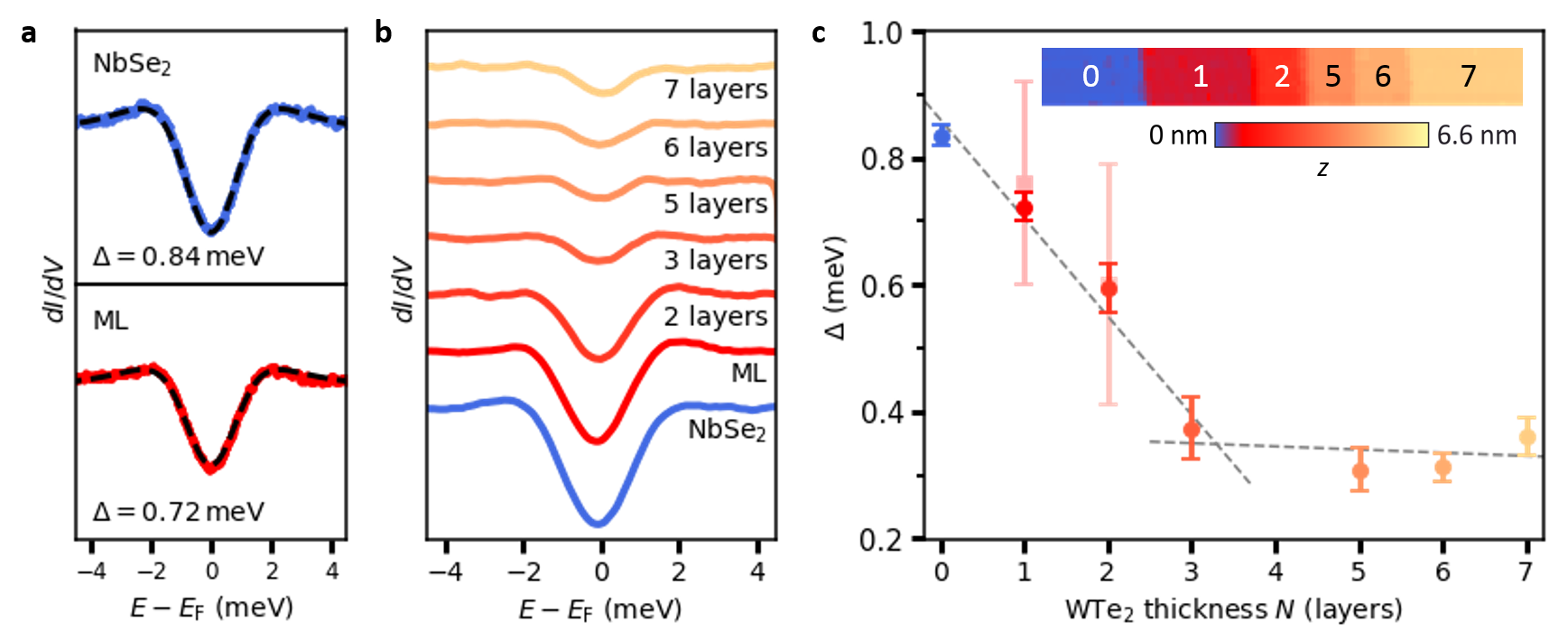
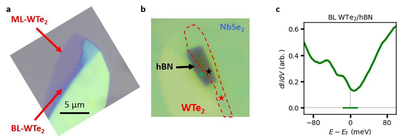
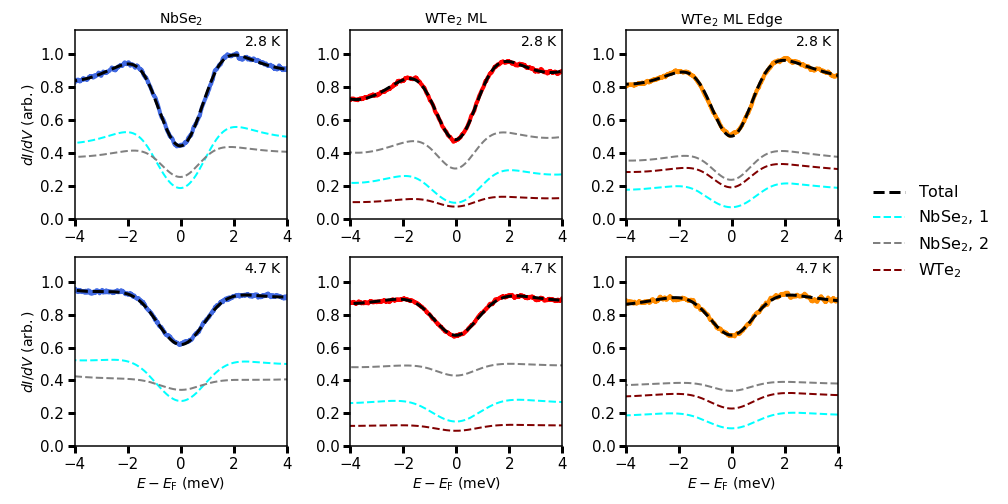
In order to confirm the proximity-induced nature of the observed superconducting gap on the WTe2, we explore its evolution as a function of WTe2 thickness. The exfoliation procedure naturally produces terraces of varying thickness in our samples, enabling thickness-dependent gap measurement within a single sample. Figure 3b shows the superconducting gap measured on terraces of different numbers of WTe2 layers , revealing that the gap decreases with increasing , as expected for decaying superconducting correlations near the boundary of a superconducting–metal interface Huang2018 . To quantify this behavior, we fit the BCS model to each of the spectra in Fig. 3b and plot the extracted gap sizes as filled circles in Fig. 3c. In the thick limit (3), we find that observed behavior shows excellent agreement with transport measurements of proximity-induced superconductivity in bulk WTe2 flakes Huang2018 ; Li2018 , extending the previous studies to the ultra-thin limit (see Supplementary Materials). For , we observe a more rapid decrease of the extracted gap as function of which may be explained by the strong variation of the electronic structure of the WTe2 in this thickness range, resulting in a larger mismatch of the WTe2 and NbSe2 Fermi surfaces and therefore a stronger dependence of the induced gap on Reeg2016 . For monolayer and bilayer WTe2, we also consider the possibility of tunneling spectra being a superposition of tunneling into WTe2 and into NbSe2 (Fig. 4b inset). To isolate the respective contributions, we performed a control experiment on a second sample, in which we placed a thick layer of insulating hBN between the WTe2 and NbSe2 to locally decouple the WTe2 (Fig. 4a, b). By comparing the measured signal at the Fermi energy of spectra taken on WTe2/hBN () and WTe2/NbSe2 (), we find that the fractional contribution of tunneling into ML WTe2 on the NbSe2 is . The NbSe2 contribution is correspondingly , i.e. the majority of the tunneling current. Knowing the relative WTe2 contribution allows us to perform a more detailed analysis of the superconducting ML WTe2/NbSe2 spectrum (Fig. 4d) by fitting a superposition of WTe2 and NbSe2 BCS spectra with the same fractional contributions, i.e. , using a BCS form for each (details in Supplementary Materials). The resulting proximity-induced gap sizes from the more detailed analysis are at and at . For bilayer WTe2 on NbSe2, using a similar procedure, we find an induced gap of . In Fig. 3c we also plot the WTe2 proximity gaps found from this more detailed fitting and find no significant deviation from those previously determined by fitting the single-gap BCS theory. This observation is in qualitative agreement with theory which predicts the proximity-induced gap to approach that of the NbSe2 as the WTe2 layer thickness goes to zero Huang2018 .
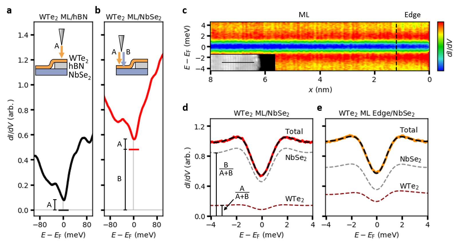
Finally, we consider the lateral variation of the superconducting gap from within the ML WTe2 to the region occupied by the edge state. Figure 4c shows spectra taken at along a line approaching the physical edge of the WTe2 monolayer, similar to that shown in Fig. 2a but over a smaller voltage range. We find that the superconducting gap is present throughout the WTe2 monolayer with only slight changes in the gap width and depth. It is apparent that a superconducting gap is present in the region in which the QSH edge state is observed in Fig. 2a (indicated by the dashed line in Fig. 4c). To determine the fractional contribution of the WTe2 edge spectrum, in Fig. 4e we perform a similar fit as we did for the spectrum away from the edge (Fig. 4d), using the same absolute NbSe2 background as in Fig. 4d, but the larger conductance for of the WTe2, corresponding to the larger tunneling conductance into the edge state at the Fermi energy (Fig. 2b). The resulting relative contribution of the edge state is and the extracted gap size is .
The observation of a superconducting gap in the edge state of monolayer 1T’-WTe2 provides strong evidence that we have created a 1D topological superconductor in a van der Waals heterostructure by proximity-induced superconductivity in the quantum spin Hall edge state. The topological nature of a superconducting QSH edge state could be explicitly demonstrated in an STM measurement by creating a boundary with a portion of the same QSH edge state in which a topologically-trivial gap has been opened Alicea2012 . This would localize Majorana zero modes at the boundary, which can be identified as a zero-bias conductance peak within the superconducting gap Jaeck2019 . Creating such a boundary is straightforward in the van der Waals material platform, e.g., by integrating a van der Waals magnetic insulator into the heterostructure shown in Fig. 1a to open a local Zeeman gap. Our work establishes the groundwork for such an experiment with a clear path toward the realization of Majorana quasiparticles. In addition, the method of sample preparation outlined in this work may be easily adapted to numerous experiments involving surface-probe studies or air-sensitive materials.
Acknowledgments.
The authors acknowledge Di Xiao, David Cobden and Xiaodong Xu for helpful discussions and Nicholas Speeney and Nicolas Iskos for assistance in the lab. B.M.H. was supported by the Department of Energy under the Early Career award program (DE-SC0018115). Crystal growth and characterization at ORNL was supported by the US Department of Energy, Office of Science, Basic Energy Sciences, Division of Materials Sciences and Engineering. The authors thank the Pennsylvania State University Two-Dimensional Crystal Consortium - Materials Innovation Platform (2DCC-MIP) which is supported by NSF DMR-1539916 for supplying further 2D materials. F.L. and D.W. were supported by the NSF DMR-1809145 for the STM measurements. The authors gratefully acknowledge NSF DMR-1626099 for acquisition of the STM instrument. S.C.d.l.B. was supported by the Department of Energy (DE-SC0018115) for fabrication of proximity-effect van der Waals heterostructures. DFT Calculations were supported by the Department of Energy under grant DE-SC0014506.
Author contributions.
F.L., D.W., R.M.F. and B.M.H. designed the experiment. F.L. and D.W. acquired the experimental data and F.L., D.W., and R.M.F. analyzed the data. F.L., D.W. and S.C.d.l.B. fabricated the samples. F.L., D.W., S.C.d.l.B., R.M.F. and B.M.H. wrote the manuscript, and all authors commented on the manuscript. J.Y. grew the WTe2 crystals. D.M. provided other van der Waals crystals used in this study. M.W. performed DFT calculations. R.M.F. and B.M.H. supervised the project.
References
- (1) S. Tang, C. Zhang, D. Wong, Z. Pedramrazi, H.-Z. Tsai, C. Jia, B. Moritz, M. Claassen, H. Ryu, S. Kahn, J. Jiang, H. Yan, M. Hashimoto, D. Lu, R. G. Moore, C.-C. Hwang, C. Hwang, Z. Hussain, Y. Chen, M. M. Ugeda, Z. Liu, X. Xie, T. P. Devereaux, M. F. Crommie, S.-K. Mo, Z.-X. Shen, Quantum spin Hall state in monolayer 1T′-−WTe2. Nat. Phys. 13, 683 (2017).
- (2) Z. Fei, T. Palomaki, S. Wu, W. Zhao, X. Cai, B. Sun, P. Nguyen, J. Finney, X. Xu, D. H. Cobden, Edge conduction in monolayer WTe2. Nat. Phys. 13, 677 (2017).
- (3) S. Wu, V. Fatemi, Q. D. Gibson, K. Watanabe, T. Taniguchi, R. J. Cava, P. Jarillo-Herrero, Observation of the quantum spin Hall effect up to 100 Kelvin in a monolayer crystal. Science 359, 76 (2018).
- (4) J. Alicea, New directions in the pursuit of Majorana fermions in solid state systems. Rep. Prog. Phys. 75, 076501 (2012).
- (5) A. Y. Kitaev, Unpaired Majorana fermions in quantum wires. Phys.-Uspekhi 44, 131 (2001).
- (6) L. Fu, C. L. Kane, Superconducting proximity effect and Majorana fermions at the surface of a topological insulator. Phys. Rev. Lett. 100, 096407 (2008).
- (7) S. Das Sarma, M. Freedman, C. Nayak, Majorana zero modes and topological quantum computation. npj Quantum Inf. 1, 15001 (2015).
- (8) M. Sato, Y. Ando, Majorana zero modes and topological quantum computation. Rep. Prog. Phys. 80, 076501 (2017).
- (9) Y. Maeno, S. Kittaka, T. Nomura, S. Yonezawa, K. Ishida, Evaluation of spin-triplet superconductivity in Sr2RuO4. J. Phys. Soc. Jpn. 81, 011009 (2012).
- (10) L. Fu, C. L. Kane, Josephson current and noise at a superconductor/quantum-spin-Hall-insulator/superconductor junction. Phys. Rev. B 79, 161408 (2009).
- (11) M.-X. Wang, C. Liu, J.-P. Xu, F. Yang, L. Miao, M.-Y. Yao, C. L. Gao, C. Shen, X. Ma, X. Chen, Z.-A. Xu, Y. Liu, S.-C. Zhang, D. Qian, J.-F. Jia, Q.-K. Xue, The coexistence of superconductivity and topological order in the Bi2Se3 thin films. Science 336, 52 (2012).
- (12) H.-H. Sun, K.-W. Zhang, L.-H. Hu, C. Li, G.-Y. Wang, H.-Y. Ma, Z.-A. Xu, C.-L. Gao, D.-D. Guan, Y.-Y. Li, C. Liu, D. Qian, Y. Zhou, L. Fu, S.-C. Li, F.-C. Zhang, J.-F. Jia, Majorana zero mode detected with spin selective Andreev reflection in the vortex of a topological superconductor. Phys. Rev. Lett. 116, 257003 (2016).
- (13) S. Hart, H. Ren, T. Wagner, P. Leubner, M. Mühlbauer, C. Brüne, H. Buhmann, L. W. Molenkamp, A. Yacoby, Induced superconductivity in the quantum spin Hall edge. Nat. Phys. 10, 638 (2014).
- (14) E. Bocquillon, R. S. Deacon, J. Wiedenmann, P. Leubner, T. M. Klapwijk, C. Brüne, K. Ishibashi, H. Buhmann, L. W. Molenkamp, Gapless Andreev bound states in the quantum spin Hall insulator HgTe. Nat. Nanotechnol. 12, 137 (2016).
- (15) X. Qian, J. Liu, L. Fu, J. Li, Quantum spin Hall effect in two-dimensional transition metal dichalcogenides. Science 346, 1344 (2014).
- (16) Z.-Y. Jia, Y.-H. Song, X.-B. Li, K. Ran, P. Lu, H.-J. Zheng, X.-Y. Zhu, Z.-Q. Shi, J. Sun, J. Wen, D. Xing, S.-C. Li, Direct visualization of a two-dimensional topological insulator in the single-layer 1T′-−WTe2. Phys. Rev. B 96, 041108 (2017).
- (17) L. Peng, Y. Yuan, G. Li, X. Yang, J.-J. Xian, C.-J. Yi, Y.-G. Shi, Y.-S. Fu, Observation of topological states residing at step edges of WTe2. Nat. Commun. 8, 659 (2017).
- (18) Y. Shi, J. Kahn, B. Niu, Z. Fei, B. Sun, X. Cai, B. A. Francisco, D. Wu, Z.-X. Shen, X. Xu, D. H. Cobden, Y.-T. Cui, Imaging quantum spin Hall edges in monolayer WTe2. Sci. Adv. 5 (2019).
- (19) V. Fatemi, S. Wu, Y. Cao, L. Bretheau, Q. D. Gibson, K. Watanabe, T. Taniguchi, R. J. Cava, P. Jarillo-Herrero, Electrically tunable low-density superconductivity in a monolayer topological insulator. Science 362, 926 (2018).
- (20) E. Sajadi, T. Palomaki, Z. Fei, W. Zhao, P. Bement, C. Olsen, S. Luescher, X. Xu, J. A. Folk, D. H. Cobden, Gate-induced superconductivity in a monolayer topological insulator. Science 362, 922 (2018).
- (21) Y. Zeng, J. I. A. Li, S. A. Dietrich, O. M. Ghosh, K. Watanabe, T. Taniguchi, J. Hone, C. R. Dean, High-quality magnetotransport in graphene using the edge-free Corbino geometry. Phys. Rev. Lett. 122, 137701 (2019).
- (22) I. Cucchi, I. Gutirrez-Lezama, E. Cappelli, S. McKeown Walker, F. Y. Bruno, G. Tenasini, L. Wang, N. Ubrig, C. Barreteau, E. Giannini, M. Gibertini, A. Tamai, A. F. Morpurgo, F. Baumberge, Microfocus laser angle-resolved photoemission on encapsulated mono-, bi-, and few-layer 1T′-−WTe2. Nano Lett. 19, 554 (2019).
- (23) P. Garoche, J. J. Veyssié, P. Manuel, P. Molinié, Experimental investigation of superconductivity in 2H-NbSe2 single crystal. Solid State Commun. 19, 455 (1976).
- (24) C. Huang, A. Narayan, E. Zhang, Y. Liu, X. Yan, J. Wang, C. Zhang, W. Wang, T. Zhou, C. Yi, S. Liu, J. Ling, H. Zhang, R. Liu, R. Sankar, F. Chou, Y. Wang, Y. Shi, K. T. Law, S. Sanvito, P. Zhou, Z. Han, F. Xiu, Inducing strong superconductivity in WTe2 by a proximity effect. ACS Nano 12, 7185 (2018).
- (25) Q. Li, C. He, Y. Wang, E. Liu, M. Wang, Y. Wang, J. Zeng, Z. Ma, T. Cao, C. Yi, N. Wang, K. Watanabe, T. Taniguchi, L. Shao, Y. Shi, X. Chen, S.-J. Liang, Q.-H. Wang, F. Miao, Proximity-induced superconductivity with subgap anomaly in type II Weyl semi-metal WTe2. Nano Lett. 18, 7962 (2018).
- (26) C. R. Reeg, D. L. Maslov, Hard gap in a normal layer coupled to a superconductor. Phys. Rev. B 94, 020501 (2016).
- (27) B. Jäck, Y. Xie, J. Li, S. Jeon, B. A. Bernevig, A. Yazdani, Observation of a Majorana zero mode in a topologically protected edge channel. Science 364, 1255 (2019).
Felix Lüpke,1∗ Dacen Waters,1∗ Sergio C. de la Barrera,1 Michael Widom,1
David G. Mandrus,2,3,4 Jiaqiang Yan,2 Randall M. Feenstra,1 Benjamin M. Hunt1†
1Department of Physics, Carnegie Mellon University, Pittsburgh, PA 15213, USA
2Materials Science and Technology Division, Oak Ridge National Laboratory, Oak Ridge, TN 37831, USA
3Department of Materials Science and Engineering, University of Tennessee, Knoxville, TN 37996, USA
4Department of Physics and Astronomy, University of Tennessee, Knoxville, TN 37996, USA
∗ These authors contributed equally
†Corresponding author. E-mail: bmhunt@andrew.cmu.edu
Supplementary Materials:
Proximity-induced superconducting gap in the quantum spin Hall edge state of monolayer WTe2
Felix Lüpke,1∗ Dacen Waters,1∗ Sergio C. de la Barrera,1 Michael Widom,1
David G. Mandrus,2,3,4 Jiaqiang Yan,2 Randall M. Feenstra,1 and Benjamin M. Hunt1†
1Department of Physics, Carnegie Mellon University, Pittsburgh, PA 15213, USA
2Materials Science and Technology Division, Oak Ridge National Laboratory, Oak Ridge, TN 37831, USA
3Department of Materials Science and Engineering, University of Tennessee, Knoxville, TN 37996, USA
4Department of Physics and Astronomy, University of Tennessee, Knoxville, TN 37996, USA
∗ These authors contributed equally
†E-mail: bmhunt@andrew.cmu.edu
S1 Sample fabrication
The newly developed sample fabrication method consists of the following steps:
-
1.
Mechanically exfoliate NbSe2 and WTe2 onto O2-plasma-cleaned SiO2/Si wafer in a nitrogen-filled glove box (Fig. S1a and b).
-
2.
Using a PPC/PDMS droplet transfer slide Wang2013-SI , pick up the NbSe2 flake, then pick up the WTe2 flake. The transfer stage temperature is C for both pick ups.
-
3.
Peel off the PPC layer from the PDMS, flip it upside down and put it onto a second transfer slide which has a PDMS droplet on it into which a hole was cut such that the heterostructure sits in the center of the hole and does not touch the PDMS.
-
4.
Place the heterostructure onto pre-evaporated gold leads (Au ()/Pd ()/Cr ()) on an SiO2/Si chip which is mounted on an STM sample plate and wire bonded to contacts sitting on the sample plate. Release the PPC by heating it to C.
-
5.
With the sample still at C, remove some of the PPC surrounding the heterostructure using a sharp needle (Fig. S1c). This step prevents the heterostructure from floating off of the gold lead in the next step.
-
6.
Transfer the sample from the glovebox into vacuum (without exposing it to air), and anneal it at C for () to remove the PPC. We perform this step using a tube furnace which has a gate valve attached to it and is vented with nitrogen. Subsequently, transfer the sample to the STM ultra-high vacuum chamber and perform a final annealing step at C for () before introducing the sample into the STM.
Using this technique, in contrast to previously reported dry-transfer techniques, the final top surface of the assembled van der Waals heterostructure is never in contact with any polymer or solvent. We find this to be crucial to achieve atomically-clean surfaces. Furthermore, sample fabrication is performed entirely in an inert gas/vacuum environment. This allows to study the pristine surfaces of highly air-sensitive materials, the only constraint being that the materials do not degrade when annealed at in vacuum.
For the samples presented in the main text, WTe2 flakes were transferred onto thick NbSe2 flakes. At this thickness, the electronic properties of the NbSe2 are bulk-like and the critical temperature below which the NbSe2 becomes superconducting is Khestanova2018-SI . Figure S1 shows optical images of the sample studied in the main text, except in Fig. 4a and b.
S2 Scanning tunneling measurements
The STM tip is approached to the WTe2/NbSe2 heterostructure using a capacitive technique adapted from Ref. 3. The commercial CreaTec STM helium bath temperature is with the ability of intermittently reaching by pumping on the cryostat. The resulting temperatures of the STM base plate are and , respectively, due to vibration isolation and optical access. The STM is equipped with an electrochemically-etched tungsten tip which was cleaned by indentation into gold prior to and in between measurements. The lock-in frequency was set to in all measurements. All superconducting gap measurements were performed at with peak-to-peak and , except in Fig. 2e where . The spectra in Fig. 2a and b were acquired using , and . In Fig. 4, tunneling parameters are: , and in (a) and , and in (b). For quantitative comparison, the spectra in Fig. 4a and b and Fig. S3c were normalized to and , respectively.
S3 Moiré effects
Figure S2a shows an STM image where both the moiré periodicity and the atomic rows of the ML WTe2/NbSe2 heterostructure can be seen. Analyzing atomic resolution images of the WTe2 and NbSe2 close to the WTe2 step edge, we find a small rotational misalignment of between the WTe2 -axis and the NbSe2 (Fig. S2b and c). The resulting moiré period can be approximated as
| (S1) |
where Å is the shorter WTe2 lattice constant, is its relative lattice mismatch with respect to the NbSe2 lattice constant () and is the rotational angle between the two materials Jung2014-SI . The resulting moiré period is which is in good agreement with the periodicity observed in the STM image. Note that the moiré period in direction of the WTe2 vector is negligibly small because the rotational misalignment of it with respect to the second NbSe2 lattice vector is large.
S4 Band gap in ML WTe2
While ARPES Crommie2017-SI and transport measurements Wu2018-SI show indications of a band gap in the electronic structure of ML WTe2, so far no hard gap has been observed in STM. Among the proposed explanations for a finite signal at the Fermi energy are defect states and substrate effects Crommie2017-SI , a charge density wave Jia2017-SI and a Coulomb gap Song2018-SI , which we discuss below. By comparing the different STM studies of ML WTe2 Jia2017-SI ; Crommie2017-SI ; Song2018-SI , defect states seem to be an unlikely explanation because the non-zero signal is observed even far away from topographic defects and the reported defect concentrations vary from study to study. While a CDW may explain the observed gap feature, the doping dependence of the band gap feature reported in Ref. 8 does not line up with a typical CDW behavior. Furthermore, the topographic CDW features are not well reproduced in reports other than in Ref. 7. Lastly, a Coulomb gap due to lateral hopping in ML WTe2 was proposed as a possible explanation Song2018-SI . This explanation is based on ML WTe2 being decoupled from the substrate, which seems reasonable due to the van der Waals stacking and small Fermi surface overlap of ML WTe2 and graphene as well as NbSe2. To understand the origin of a possible Coulomb gap in more detail, we consider tip-induced band bending (TIBB) to play a crucial role. TIBB can have a significant effect on the measured spectra and is known to lead to a finite signal in the band gap Fennstra1994-SI . The 2D analog of 3D TIBB is a local band shift in the 2D layer. As a result, there is no additional confinement of states in the -direction but only in the - plane, i.e. a laterally extended circular potential well. The depth of the potential well increases with decreasing tip-sample distance and decreasing STM tip work function and results in a local accumulation of charges at the position of the STM tip, i.e. a downward band shift. In the context of TIBB, the observed dip in the finite signal at the Fermi energy can be explained as a Coulomb gap associated with the accumulation layer that is formed in the potential well. TIBB may also explain why the in-gap signal and the signature of the Coulomb gap is weak in Ref. 5: in their experiments the current setpoint was lower (and the work function of their tip may have been higher), producing less TIBB and therefore fewer electrons in the accumulation layer compared to our results and Refs. 7; 8. Furthermore, the presence of a tip-induced electron accumulation layer in the WTe2 can explain the reported conduction and valence band overlap extracted from quasi-particle interference (QPI) measurements in Ref. 8 which is in contrast to ARPES results Crommie2017-SI : with the finite signal in the band gap originating from the tip-induced electron accumulation layer, it is expected that the QPI of these states will yield wave vectors corresponding to the down-shifted conduction band states. As a result, QPI is expected to show conduction band wave vectors down to voltages beyond the actual conduction band edge and persist until they are dominated by the valence band conductance. In summary, we believe that TIBB may explain the majority of gap features reported in the literature.
S5 Spectra fitting
The finite-temperature differential conductance function that we fit to the spectroscopic data is the density of states convolved with the derivative of the Fermi function, i.e.
| (S2) |
where is the density of states of the sample and the density of states in the tip is assumed to be uniform. In standard BCS theory, the density of states is given by
| (S3) |
where is the gap size of the superconductor and is the normal state density of states, which is typically assumed to be constant. However, in experiments the differential conductance signal often shows a non-constant normal state conductance around the Fermi energy. To achieve representative fits of the superconducting gaps, we therefore allow for a normal state conductance background given by a low-order polynomial function which we fit simultaneously with the BCS gap function (this is then divided out of the superconducting gap spectra presented in the main text Figs. 2, 3, and 4). We fit the NbSe2 spectra using a two-gap model Khestanova2018-SI , which we find provides good fits at all temperatures. The density of states for the two-gap model is given by
| (S4) |
First, we fit data of Ref. 10 acquired at , yielding gaps of and meV (and a tip temperature of ). The amplitudes of the large-gap and small-gap terms are expressed by parameters and , with a value of found from this fit. This same value of is then used in fits to our own NbSe2 spectra, shown in Fig. S4. The resulting gap sizes are meV and meV with tip temperature of at a base plate temperature of , and gaps of and meV with tip temperature of at a base plate temperature of . We find that the temperature dependence of the larger of these NbSe2 gap values matches very well to the universal temperature behavior of a BCS superconducting gap. The temperature dependence of the smaller gap, however, does not agree as well with the universal BCS prediction. The sample temperatures in our experiments, extracted from the known temperature dependence of the NbSe2 gaps, are approximately above our measured STM base plate temperatures.
| Parameter | 2.8 K | 4.7 K | |
|---|---|---|---|
| NbSe2 | |||
| (fixed) | |||
| WTe2 monolayer | |||
| WTe2 ML edge | |||
| (fixed) | |||
| WTe2 bilayer | |||
| WTe2 three layers | |||
| WTe2 five layers | |||
| WTe2 six layers | |||
| WTe2 seven layers | |||
Fitting of WTe2 monolayer and monolayer edge on NbSe2. Moving to the spectra acquired on the monolayer and the monolayer edge of WTe2 on NbSe2 and comparing those spectra to ones acquired on WTe2 on hBN (Fig. 4 of the main text), we find that there is a significant contribution to the tunneling current from the underlying NbSe2. We therefore fit our ML WTe2 spectra with a three-gap model, two gaps of known size from the NbSe2 and one induced gap from the WTe2, , the size of which is determined by fitting
| (S5) |
We fix the fractional contribution of the NbSe2, , by comparing the value of the observed conductance at the Fermi energy for ML WTe2 on NbSe2 and for ML WTe2 on hBN. Importantly, for the NbSe2 contribution, the relative amplitudes of the large-gap and small-gap terms is expected to differ from the deduced above from bare NbSe2, since the wave functions of the respective states will have varying decay constants as they extend through the WTe2 and out into the vacuum. We therefore let vary in the fits of the WTe2 spectra. The tip temperatures are known from the fits to the bare NbSe2 spectra and are fixed for fits of the spectra taken on the WTe2.
To maximally constrain the fits, we simultaneously fit the spectra acquired at temperatures and , thus having three unknowns in total to fit the two spectra: the induced superconducting gap size for each, and the relative amplitude of the NbSe2 large-gap and small-gap terms (i.e. the same value in both spectra). Using the best fit, midpoint values for all other “auxiliary” parameters (NbSe2 gap sizes, sample temperatures, WTe2 fractional contribution), we find values for the proximity-induced gaps in the WTe2 of (at ) and (at ) and (Fig. S4). To properly estimate error bounds for the induced gap, we further perform fits at the minimum and maximum values of the error range of all auxiliary parameters, thus yielding final values for the proximity-induced gaps for ML WTe2 far from an edge of and , respectively at and , and .
For the case of the WTe2 ML edge on NbSe2, we fit a spectrum acquired at using the known NbSe2 gaps and known tip temperature, with determined to be by comparison of the edge spectrum (Fig. 2b) with those of the non-edge WTe2 on NbSe2 and WTe2 on hBN (we make this indirect comparison because it is not possible to measure ML edge spectra on hBN, which would require there to be an exposed insulating hBN surface). We fit the edge spectrum using the value of , which we obtained from the monolayer fits. The resulting fit is shown in Fig. S4, with induced gap of . For the case of acquisition temperature (not shown), the same procedure yields an induced gap of .
We note that we are not able to achieve good fits of our WTe2 data if we assume a constant WTe2 contribution, i.e. one that does not have a superconducting gap.
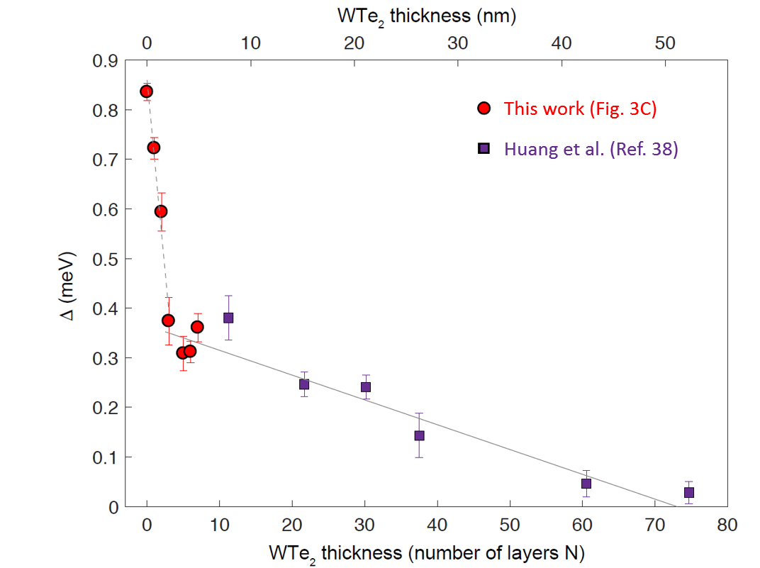
Fitting of multilayer WTe2 on NbSe2. We now consider thicker WTe2 on NbSe2, for which we have measured tunneling spectra at (Fig. 3). For or more layers of WTe2 we fit the observed spectra with a single-gap model (Eq. S3), obtaining proximity-induced gaps in good agreement with the thickness-trend found in prior measurements of layers of WTe2 on SiO2 Huang2018-SI as shown in Fig. S5. We conclude that the tunneling contribution of NbSe2 to the observed spectra is negligible for . For the case of bilayer WTe2 on NbSe2, as for monolayer WTe2/NbSe2, we must estimate the contribution of the NbSe2 to the bilayer WTe2/NbSe2 spectrum. To do so, we have measured a spectrum of bilayer WTe2 on hBN (Fig. S3c), from which we find the tunneling conductance at the Fermi energy to be larger than that for ML WTe2 on hBN, thus implying a lower bound for the contribution of WTe2 itself to the spectrum of bilayer WTe2 on NbSe2 of , with the additional conservative assumption that the total tunneling current into the NbSe2 on BL WTe2/NbSe2 is the same as on ML WTe2/NbSe2 (in general we expect the total tunneling into BL WTe2/NbSe2 to be less.) We therefore consider a range of WTe2 fractional contributions for the bilayer case extending from 0.25 to 1.0. For the fractional magnitude of the NbSe2 large-gap term, in the discussion above we found values of and for zero and one WTe2 layer, respectively; thus, for two layers of WTe2 we assume values in the range . Within these parameter ranges, we find a proximity-induced gap for the bilayer WTe2 to be in the range , or . Our fit results are summarized in Table 1.
S6 Density Functional Theory Calculations
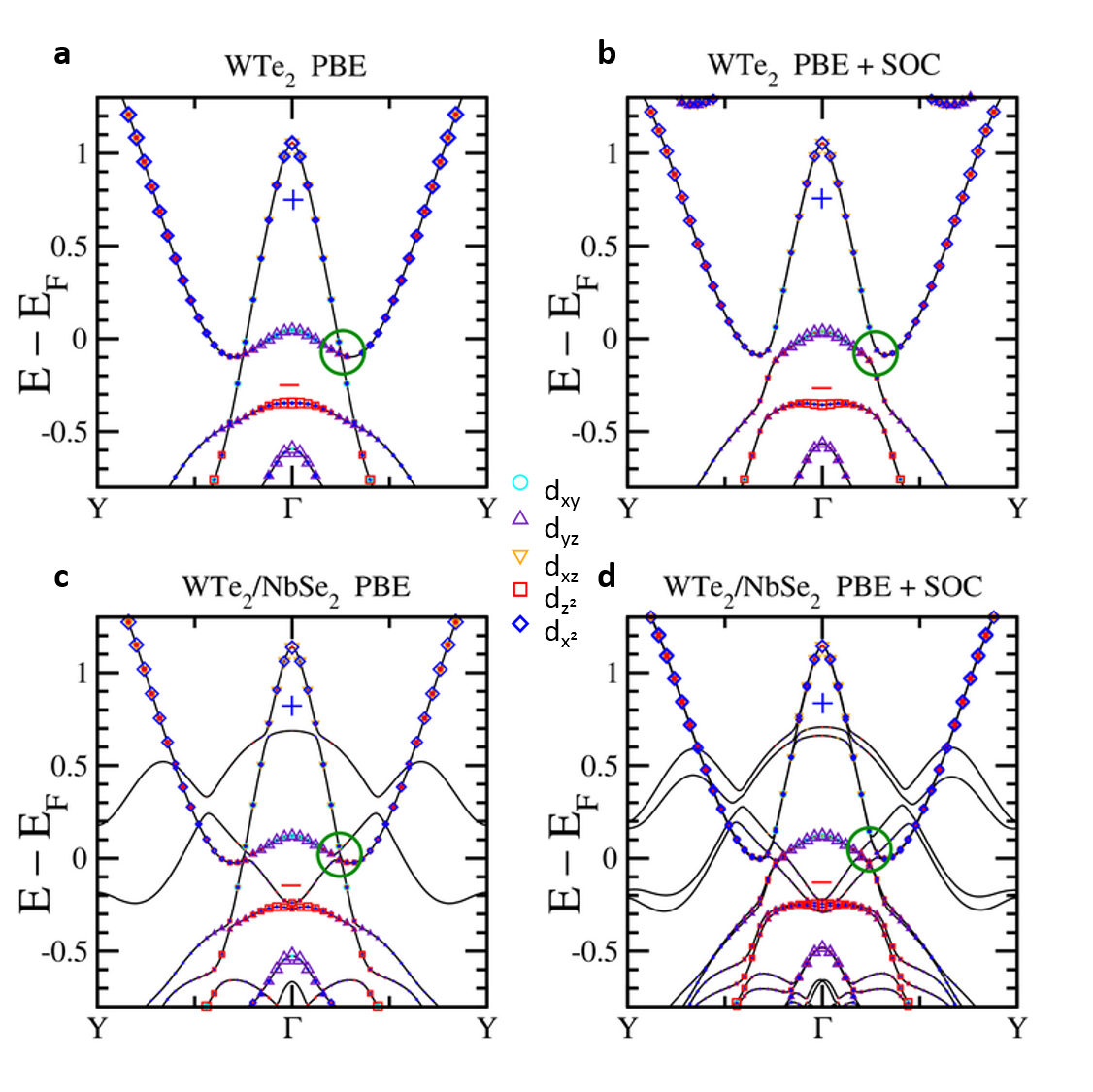
We performed band structure calculations (Fig. S6) using density functional theory (DFT) in the generalized gradient approximation Perdew1996-SI utilizing the projector augmented wave method as implemented in VASP Kresse1999-SI . Lattice constants were set to orthorhombic WTe2 values (Å and Å) for both the ML and the WTe2/NbSe2 bilayer, while we took Å to allow sufficient vacuum. Atomic coordinates were relaxed holding the lattice constants fixed prior to calculating the band structure. The results for the freestanding WTe2 monolayer, with and without spin-orbit-coupling (SOC) are shown in Fig. S6a and b. Note that in WTe2 the bands near the Fermi energy originate mostly from the W atoms, the orbital character of which we plot as symbols as indicated in the figure legend. The calculations are in excellent agreement with previously reported band structures of 1T’-WTe2. Especially, the inversion of bands with opposite parity is reproduced (marked as ”+” and ”-” in the figures). Note that the size of the gap, which opens when including SOC into the calculations is under predicted in DFT.
Next, we perform calculations which, in addition to the ML WTe2, include a layer of NbSe2 to model the present sample system. For this purpose, we construct a heterostructure unit cell which includes unit cells of NbSe2 and unit cells of WTe2. The NbSe2 lattice parameter is adjusted such that the constructed unit cells match in size. We then let the structure relax, before calculating the supercell band structure, with and without SOC. Figures S6c and d show the resulting heterostructure bands, where we plot the W orbital character as symbols as before. The NbSe2 bands near the Fermi energy are dominated by Nb which we plot without symbols. From the calculations, we find that the NbSe2 has little effect on the the WTe2 single-particle electronic structure, i.e. we observe no significant shifts of bands relative to each other and the band inversion is still present. There is only a small rigid upward shift of the WTe2 bands () with respect to the calculated freestanding WTe2 due to an NbSe2 band near the Fermi level. Furthermore, we observe a slight hybridization between bands that originate in the NbSe2 and the even parity conduction band of the WTe2, but only at an energy well above the Fermi level. Note that the band splitting in Fig. S6d comes from the broken inversion symmetry due to the presence of the NbSe2 which lifts the spin degeneracy of the bands when SOC is included. In conclusion, we find that the WTe2 single-particle band structure, including the band inversion and therefore the QSH state, is preserved in the WTe2/NbSe2 heterostructure.
References
- (1) L. Wang, I. Meric, P.Y. Huang, Q. Gao, Y. Gao, H. Tran, T. Taniguchi, K. Watanabe, L.M. Campos, D.A. Muller, J. Guo, P. Kim, J. Hone, K.L. Shepard, and C.R. Dean, One-Dimensional Electrical Contact to a Two-Dimensional Material. Science 342, 614–617 (2013).
- (2) E. Khestanova, J. Birkbeck, M. Zhu, Y. Cao, G.L. Yu, D. Ghazaryan, J. Yin, H. Berger, L. Forró, T. Taniguchi, K. Watanabe, R.V. Gorbachev, A. Mishchenko, A. K. Geim, and I. V. Grigorieva, Unusual suppression of the superconducting energy gap and critical temperature in atomically thin NbSe2. Nano Lett. 18, 2623–2629 (2018).
- (3) G. Li, A. Luican, and E.Y. Andrei, Self-navigation of a scanning tunneling microscope tip toward a micron-sized graphene sample. Rev. Sci. Instrum. 82, 073701 (2011).
- (4) J. Jung, A. Raoux, Z. Qiao, A. H. MacDonald, Ab initio theory of moiré superlattice bands in layered two-dimensional materials. Phys. Rev. B 89, 205414 (2014).
- (5) S. Tang, C. Zhang, D. Wong, Z. Pedramrazi, H.-Z. Tsai, C. Jia, B. Moritz, M. Claassen, H. Ryu, S. Kahn, J. Jiang, H. Yan, M. Hashimoto, D. Lu, R. G. Moore, C.-C. Hwang, C. Hwang, Z. Hussain, Y. Chen, M. M. Ugeda, Z. Liu, X. Xie, T. P. Devereaux, M. F. Crommie, S.-K. Mo, Z.-X. Shen, Quantum spin Hall state in monolayer 1T′-−WTe2. Nat. Phys. 13, 683 (2017).
- (6) S. Wu, V. Fatemi, Q. D. Gibson, K. Watanabe, T. Taniguchi, R. J. Cava, P. Jarillo-Herrer, Observation of the quantum spin Hall effect up to 100 Kelvin in a monolayer crystal. et al., Science 359, 76 (2018).
- (7) Z.-Y. Jia, Y.-H. Song, X.-B. Li, K. Ran, P. Lu, H.-J. Zheng, X.-Y. Zhu, Z.-Q. Shi, J. Sun, J. Wen, D. Xing, S.-C. Li, Direct visualization of a two-dimensional topological insulator in the single-layer 1T′-−WTe2. Phys. Rev. B 96, 041108 (2017).
- (8) Y.-H. Song, Z.-Y. Jia, D. Zhang, X.-Y. Zhu, Z.-Q. Shi, H. Wang, L. Zhu, Q.-Q. Yuan, H. Zhang, D.-Y. Xing, S.-C. Li, Observation of coulomb gap in the quantum spin Hall candidate single-layer 1T′-−WTe2. Nat. Commun. 9, 4071 (2018).
- (9) R. M. Feenstra, Tunneling spectroscopy of the (110) surface of direct-gap III-V semiconductors. Phys. Rev. B 50, 4561 (1994).
- (10) I. Guillamon, H. Suderow, F. Guinea, S. Vieira, Intrinsic atomic-scale modulations of the superconducting gap of 2H−-NbSe2. Phys. Rev. B 77, 134505 (2008).
- (11) C. Huang, A. Narayan, E. Zhang, Y. Liu, X. Yan, J. Wang, C. Zhang, W. Wang, T. Zhou, C. Yi, S. Liu, J. Ling, H. Zhang, R. Liu, R. Sankar, F. Chou, Y. Wang, Y. Shi, K. T. Law, S. Sanvito, P. Zhou, Z. Han, F. Xiu, Inducing strong superconductivity in WTe2 by a proximity effect. ACS Nano 12, 7185 (2018).
- (12) J. P. Perdew, K. Burke, M. Ernzerhof, Generalized gradient approximation made simple. Phys. Rev. Lett. 77, 3865 (1996).
- (13) G. Kresse, D. Joubert, From ultrasoft pseudopotentials to the projector augmented-wave method. Phys. Rev. B 59, 1758 (1999).