Superconductivity in twisted Graphene heterostructures
Abstract
We study the low-energy electronic structure of heterostructures formed by one sheet of graphene placed on a monolayer of . We build a continuous low-energy effective model that takes into account the presence of a twist angle between graphene and , and of spin-orbit coupling and superconducting pairing in . We obtain the parameters entering the continuous model via ab-initio calculations. We show that despite the large mismatch between the graphene’s and ’s lattice constants, due to the large size of the ’s Fermi pockets, there is a large range of values of twist angles for which a superconducting pairing can be induced into the graphene layer. In addition, we show that the superconducting gap induced into the graphene is extremely robust to an external in-plane magnetic field. Our results show that the size of the induced superconducting gap, and its robustness against in-plane magnetic fields, can be significantly tuned by varying the twist angle.
I Introduction
Transition metal dichalcogenides (TMDs) are extremely interesting materials due to their unique electronic properties Ramasubramaniam (2012); Latzke et al. (2015); Cazalilla et al. (2014); Wang et al. (2012, 2015); Gmitra et al. (2016); Duerloo et al. (2014); Ugeda et al. (2015); Xi et al. (2015a, b); Xu et al. (2014) and the fact that in recent years experimentalists have been able to isolate and probe TMD films only few atoms thick, down to the monolayer limit. Some TMDs monolayers, like and , are insulators with gaps of the order of 1.5-2 eV. Other TMDs monolayers, such as , , , are metallic at room temperature and superconducting at low temperature. One feature that all TMDs have in common is a strong spin-orbit coupling (SOC). In monolayer TMDs the strongest effect of the SOC is a spin-splitting of the conduction and valence bands around the , and , points of the Brillouin zone (BZ) Böker et al. (2001); Ding et al. (2011); Mak et al. (2010). For the TMDs that are superconducting at low temperature, such a spin splitting causes the superconducting pairing to be of the Ising type Xi et al. (2015a) and therefore extremely robust to external in-plane magnetic fields Dvir et al. (2018a); Lu et al. (2015); Saito et al. (2015); de la Barrera et al. (2018). The ability of metallic TMDs to exhibit superconductivity even in the limit in which they are only one-atom thick, and the robustness of such superconducting state to external magnetic fields make them very interesting systems both from a fundamental point of view and for possible applications.
Recent advances in fabrication techniques have made possible the realization of van der Waals (vdW) heterostructures obtained by stacking crystals that are only few atoms thick Dean et al. (2010); Geim and Grigorieva (2013) In these structures the different layers are held together by van der Waals forces. As a consequence the crystals that can be used to create the structures, and their stacking configuration, are not limited to the configurations allowed by chemical bonds. This makes possible the realization of systems with unique properties such as graphene–topological-insulator heterostructures in which graphene has a tunable spin-orbit coupling depending on the stacking configuration Kou et al. (2013); Zhang et al. (2016, 2014); Zalic et al. (2017); Rodriguez-Vega et al. (2017).
In graphene the conduction and valence bands touch at the corners ( and points) of the hexagonal BZ, and around these points the electrons behave as massless Dirac Fermions Novoselov et al. (2005); Castro Neto et al. (2009). This fact makes graphene an ideal semimetal in which the polarity of the carriers can easily be tuned via external gates. In addition, graphene has a very high electron mobility due to its very low concentration of defects and the fact that electron-phonons scattering processes do not contribute significantly to the resistivity for temperatures as high as room temperature Rossi et al. (2009); Das Sarma et al. (2011); Rodriguez-Vega et al. (2014). All these features make graphene an ideal system to probe, via tunneling setups, other materials and to realize novel vdW heterostructures with tunable properties. In particular, the fact, that the low energy states of graphene, in momentum space, are located just at the points of its BZ, in vdW structures implies that by simply varying the twist angle, graphene can be used as a momentum selective probe of the electronic structure, and properties, of the substrate. The work that we present below is an example of such momentum-selective probing capability of graphene. In monolayer the Fermi surface (FS) is formed by a pocket around the point, and pockets around the , and points. Contrary to bulk , in monolayer there is no selenium-like FS pocket around the point. As a consequence monolayer is expected to be a single-gap superconductor with the same gap at the pocket as at the pockets Khestanova et al. (2018). However, the and pockets differ in the magnitude, and dependence around the pocket, of the spin-splitting induced by the spin-orbit coupling. The splitting is much larger for the pockets and therefore the superconducting gap for these pockets is much more robust to external in-plane magnetic fields than for the pocket. As we show below a graphene- heterostructure allows to probe separately ’s states around the point, and point simply by tuning the relative twist angle between graphene and and therefore to study the difference between pockets of the interplay between spin-orbit coupling and superconducting pairing.
In this work we study vdW heterostructures formed by graphene and monolayer . Our results show that despite the large mismatch between the lattice constants of graphene and in these structures a large superconducting pairing can be induced into the graphene layer. In addition, we show how such pairing depends, both in nature and structure, on the stacking configuration. Our results are relevant also to other graphene-TMD heterostructures such as the ones that can be obtained by replacing the monolayer by a monolayer of , , or that have also been shown to be superconducting at low temperature Leroux et al. (2012); Kačmarčík et al. (2010); de la Barrera et al. (2018); Navarro-Moratalla et al. (2016) and show how graphene can be used to probe in these systems the momentum-dependent superconducting gap and in particular its multiband structure.
II Method
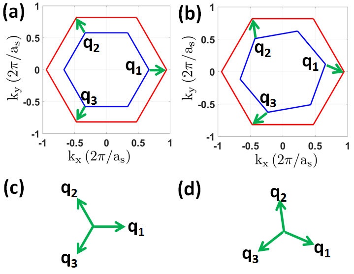
In graphene the carbon atoms are arranged in a 2D hexagonal structure formed by two triangular sublattices, and , with lattice constant , with the carbon-carbon atomic distance. The 2D structure of is also formed by two triangular sublattices. One of the sublattices is formed by the Nb atoms, the other by two Se atoms symmetrically displaced by a distance above and below the plane formed by the Nb atoms. The lattice constant of is . Ding et al. (2011). Figure 1 shows the Brillouin zone of graphene and . In this figure and in the remainder we take to be in the direction connecting the valley with its time-reversed partner . Figure 1 (a) shows the relative orientation of the graphene’s and ’s BZs for the case when the twist angle is zero and Figure 1 (b) for a case when .
To obtain the electronic structure of the graphene- structure for a generic twist angle and in the presence of superconducting pairing in the , we first need to estimate the charge transfer between the graphene layer and , and the strength of the tunneling between graphene and the monolayer. To this effect we first obtain via ab-initio the electronic structure of a commensurate graphene- structure. Let , , be the primitive lattice vectors for , and , , the primitive vectors for graphene, with and the unit vectors in the and direction, respectively. In a commensurate stacking configuration the primitive vectors satisfy the equation:
| (1) |
where are four integers constrained by the following second order Diophantine equation:
| (2) |
Given that the lattice constant of graphene and NbSe are highly incommensurate with respect to each other, Eq. 1 (or, equivalently, Eq. 2) can only be satisfied for structures with primitive cells comprising a very large number of atoms (1000). It is computationally extremely expensive to study structures with such large primitive cells using ab-initio methods. For this reason we allow for few percents strain of the graphene’s lattice so that Eq. 1 (or, equivalently, Eq. 2) can be satisfied for structures with primitive cells comprising 100 atoms or less. In general the relative strain of the graphene’s and NbSe2’s lattices will depend on the specific structure considered. We did not perform an energy minimization analysis and chose to strain graphene rather than NbSe2 for convenience. This is justified considering that the amount of charge transfer between the graphene layer and NbSe2, and the magnitude of the graphene-NbSe2 tunneling strength, are not expected to be affected by a small change of the graphene’s or NbSe2’s lattice constant
The ab-initio calculation were performed using the Quantum-Espresso package Giannozzi et al. (2009, 2017). We use full-relativistic ultrasoft pseudopotentials with the wavefunction kinetic energy cutoff of 50 Ry. We adopted the Perdew-Burke-Ernzerhof (PBE) Perdew et al. (1996) as the exchange and correlation functional. We set the vacuum thickness equal to to isolate the heterostructure and avoid the interactions between the periodic layers along the direction, (), perpendicular to the layers. The interlayer distance between graphene and was obtained by full relaxation in the z-direction. The total energy was calculated by using a Monkhorst-Pack scheme grid for the points.
After having obtained the amount of charge transfer and the strength of the tunneling between the graphene layer and via ab-initio, we use a continuum model Mele (2010, 2012); Bistritzer and MacDonald (2011); Zhang et al. (2014) to obtain the low-energy spectrum of the graphene- heterostructure for different values of the twist angle . In general, the Hamiltonian describing the graphene- heterostructure can be written as: where is the Hamiltonian for graphene, is the Hamiltonian for and is the term describing tunneling processes between graphene and .
In graphene the low energy states are located at the and points of the BZ: , (and equivalent points connected by reciprocal lattice wave vectors). Close the and points in graphene the electrons, at low energies, are well described as massless Dirac fermions with Hamiltonians , , where
| (3) | ||||
| (4) |
() is the creation (annihilation) operator for an electron, in the graphene sheet, with spin and two-dimensional momentum , is a wave vector measured from (), m/s is graphene’s Fermi velocity, graphene’s chemical potential, and , () are the Pauli matrices in sublattice and spin space, respectively. As a consequence, when considering the states of graphene close to the () point we have ().
In the low energy states are located close to the , , and points of the BZ: , (and equivalent points connected by reciprocal lattice wave vectors). Close the point the effective low-energy Hamiltonian for takes the form , where () is the creation (annihilation) operator for an electron in with momentum and spin , and is the effective low energy Hamiltonian matrix for the conduction band of . By fitting the ab-initio results we obtain:
| (5) |
where
| (6) |
, and , , are constants:
| (7) |
Close to the corners of the BZ of , the and points, for we have , , where is now a wave vector measured from the , point, respectively, and
| (8) | ||||
| (9) |
where,
| (11) |
and , , , , , are constants that we extracted from the ab-initio results for an isolated monolayer of :
| (12) |
Let , , be the wave vector of an electron in graphene, , respectively. In the remainder we consider only momentum and spin conserving tunneling processes. Conservation of crystal momentum requires
| (13) |
where and are reciprocal lattice vectors for graphene and respectively. For the purpose of developing a continuum low energy model for a graphene- heterostructure it is more convenient to consider the twist angle as relative twist between BZ’s, as shown in Fig. 1. For the point of graphene’s and ’s BZs are on the same axis. Depending on the value of we can have two situations: the low energy states of graphene, in momentum space, are close to ’s Fermi pockets around the and points, or, considering ’s extended BZ, to ’s Fermi pocket around the point. In the first case the conservation of the crystal momentum, Eq. (13), takes the form:
| (14) |
where are momentum wave vectors measured from and , respectively. By replacing , , with , and in Eq. (14) we obtain the momentum conservation equation valid for momenta taken around the points. In the second case Eq. (13) takes the form:
| (15) |
and similarly for momenta around .
The conservation of the crystal momentum implies that the tunneling term takes the form:
| (16) |
where is the position of the carbon atom on sublattice within the primitive cell of the graphene sheet. For sublattice , for sublattice , with the carbon-carbon distance.
Considering that, as shown in table 1, the separation between the graphene sheet and is much larger than the interatomic distance in each material, in momentum space, the tunneling amplitude decays very rapidly as a function of Bistritzer and MacDonald (2011) and so in Eq.(16) we can just keep the terms for which is smallest, i.e., restrict the sum to and the two that map () to the two other equivalent points in the BZ and set . The sum over is restricted by the fact that we only need to keep terms for which the graphene’s and ’s states have energy separated by an amount of the order of .
Let . The above considerations imply that for the case when the and are close we only need to keep the terms for which , given that these are the terms for which that satisfies Eq. (14) is smallest. Due to the symmetry of the hexagonal structure there are three equivalent points, , , , (and points), i.e. two reciprocal lattice wave vectors connecting equivalent corners of the BZ. There are three vectors () such that . is obtained by taking and , by taking , , and by taking , .
When the graphene’s low energy states are close to the pocket of ’s second BZ the smallest possible value of is with . As before, considering the symmetry, there are three vectors with this magnitude: obtained by taking , , obtained by taking , , and obtained by taking , ,
By retaining only the tunneling terms for which is largest, when considering the graphene states close to the point so that , we can rewrite as
| (17) |
with:
| (20) |
| (23) |
| (26) |
In the remainder, supported by DFT results, we take to be the same both when the graphene’s low energy states tunnel into states around the () point and the point of . Let . When we can develop a perturbative approach in which is the small parameter Lopes dos Santos et al. (2007); Bistritzer and MacDonald (2011): terms of order correspond n-tuple tunneling processes. For our situation, as we show in the following section, and so we can retain just the lowest order terms in .
It is convenient to define the following spinors:
For the case when the graphene’s FS overlaps with the ’s pocket close to the point, we can then express the Hamiltonian for the graphene- system as with
| (31) |
For the case when we consider graphene states close to the point, so that , the expression of the Hamiltonian matrix for the graphene- system, within the approximations described above, can be obtained from Eq. (31) by doing the following substituions: , , , and noticing that . Similarly, when the low energy states of graphene are close to the point of the Hamiltonian () is obtained from the expression (31) for via the substitutions (), and (.
Including the superconducting pairing, the effective low-energy Hamiltonian for for states close to the point takes the form
| (32) |
where is the Nambu spinor ,
| (35) |
is given by Eq. (5), and is the size of the superconducting gap of close to the point.
For states close to , including the superconducting pairing, the Hamiltonian for becomes
| (36) |
where now () is understood to be measured from (), and
| (39) |
, are given by Eq. (8).
For monolayer the superconducting gap is expected to have the same value, , on the and pocket. In the remainder we conservatively assume meV Khestanova et al. (2018).
The Hamiltonian for the graphene- system including the superconducting pairing in . For the case when is close to the Hamiltonian becomes , with ),
| (42) |
and
| (47) |
where is the zero matrix with rows and columns.
Similarly, for the case when the low energy states of graphene are close to the point of the extended BZ of the Hamiltonian for the whole system becomes , with ),
| (50) |
III Results
The large lattice mismatch between graphene and would suggest that even in the absence of any twist angle the electronic states of the two systems would not hybridize. However, this does not take into account the large size of ’s Fermi pockets. As shown in Fig. 2 there is a large set of values of for which the Dirac point of graphene intersects the ’s FS either around the points, or around the point in the repeated zone scheme. For these points the electronic states of graphene and are expected to hybridize.
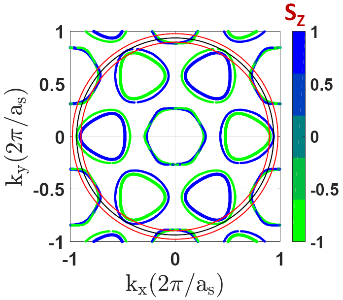
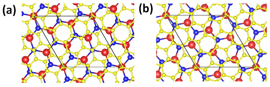
From the results shown in Fig. 2 we see that for small values of , we can expect that the graphene’s low energy states close to the Dirac point will hybridize with the ’s states close to the point. For values of close to we see that graphene’s states will hybridize with ’s states close to the point. For this reason, to estimate the charge transfer and the strength of the graphene- tunneling in the two situations, we performed ab-initio calculations for a commensurate heterostructure with , and one with . The parameters identifying these commensurate structures are given in table 1 and the corresponding primitive cells are shown in Fig. 3.
The ab-initio calculations return the band structure shown in Fig. 4, 5. In these figures the dashed blue lines show the bands of isolated graphene. The left panels show the results obtained without including spin-orbit effects and the right panels the results obtained taking into account the presence of spin orbit coupling. Panels (c) and (d) show an enlargement at low energies of the results shown in panels (a) and (b).
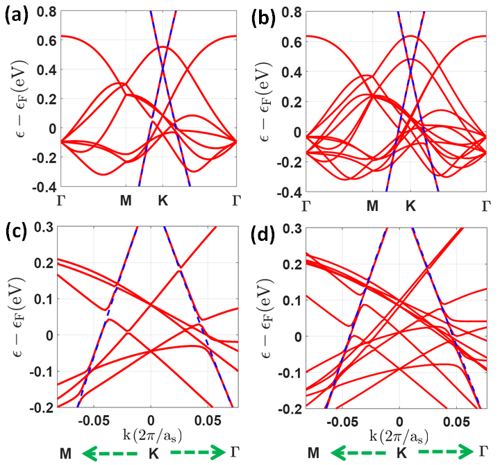
The results of Fig. 4, 5 clearly show that there is a significant charge transfer between graphene and monolayer resulting in hole doping of the graphene sheet corresponding to a Fermi energy of about -0.4 eV. They also show that the amount of charge transfer does not depend on the value of the twist angle . Considering the finite extension of the graphene’s FS due to the charge-transfer shown in Fig. 4 5 between and graphene, we obtain that there is a significant range of values of for which the graphene’s FS intersects the FS and for which we can then expect non-negligible hybridization of the graphene’s and states. This is shown in Fig. 2 in which the red circles delimit the boundaries of the graphene’s FS as is varied. Table 2 shows the range of values of extracted from Fig. 2 for which the graphene’s FS is expected to intersect either one of the ’s FS pockets around the () point, or around the point. In this table () is the angle in the middle of the range () of angles for which the graphene’s FS intersects the ’s FS.
| TMD (1L) | ||||
|---|---|---|---|---|
The ab-initio results allow us also to estimate the strength of the tunneling between graphene and . In Figs. 4 (c), (d), 5 (c), (d) we can see the avoided crossings close to the Fermi energy between the graphene’s and ’s bands. The amplitude of such crossings provides an estimate of the tunneling strength between the graphene sheet and the monolayer of . We find that both for the case when the graphene’s FS intersects the ’s pocket around the point and when it intersects the ’s FS pocket around the point, meV and so in the remainder we set meV.
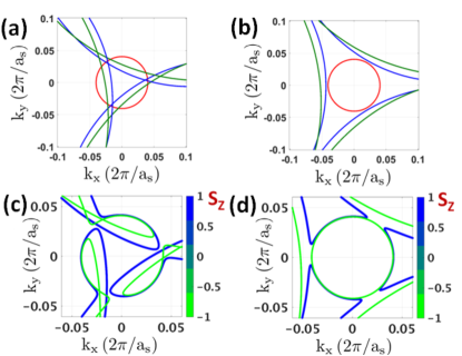
We first consider the case when graphene’s FS intersects the FS pocket of close to the point, i.e. , and . Figure 6 shows the results for the FS of the hybridized system in the limit when no superconducting pairing is present in : the left (right) column shows the FS around the () of graphene. Figure 6 (a), (b) show the relative position in momentum space of graphene’s FS and ’s FS for the case when and , taking into account the “folding” of the ’s FS pockets due to the fact that the three () corners of the BZ are equivalent. The graphene FS is shown in red and the spin splitted ’s FS in blue and green. We use this color-convention throughout this work. A zoom closer to the graphene’s point, Figs 6 (c), (d), clearly shows the overlap of the graphene’s FS with the ’ FS pockets. When the graphene’s and ’s states hybridize giving rise to the reconstructed FSs shown in Fig. 6 (e), (f). Figures 6 (e), (f) show that the graphene’s FS, due to the hybridization with , becomes spin split.
Figure 7 shows the results for the case when , left column, and , right columns. For these values of the twist angle the low energy states of graphene are still close to the low energy states of located around ’s points. For the graphene’s and ’s low energy states are still close enough (in momentum and energy) that, for meV, the hybridization is strong enough to significantly modify the FS of the combined system, as shown in Fig 7 (c), obtained setting . For the graphene’s and ’s FSs are tangent at isolated points as shown in Fig. 7 (b). As a consequence, when the states at the FS of graphene and only hybridize around these “tangent-points”, as shown in Fig. 7 (d) obtained for meV and .

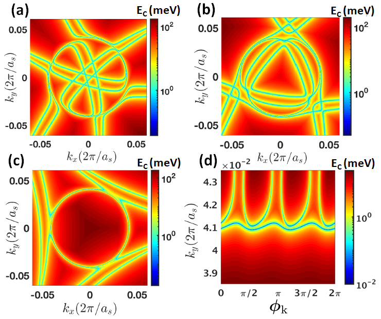
We now consider the case when a superconducting gap is present in . We find that for the FS is completely gapped but the gap is not uniform. Figure 8 (a) shows the lowest positive electron energy, , as a function of . The smallest value of corresponds to the induced superconducting gap . For we find meV. By calculating the smallest value of for each angle we obtain the angular dependence of . This is shown in Fig. 8 (b) for the case when the twist angle is zero. We see that is strongly anisotropic, with a symmetry, a reflection of the structure of the reconstructed FS, Fig. 6 (e), 7 (c).
As the twist angle increases decreases becoming vanishing small for . Figure 8 (c) shows when . From this figure we see that the location where is minumum appears to correspond to the original graphene’s FS for which . A closer inspection however reveals small oscillations as a function of , as shown in Fig. 8 (d) where is plotted as function of and for a small range of centered at .
We now consider the case when the graphene’s FS touches, in the extended BZ, the ’s FS pocket around the point. Figure 9 shows the results when , situation for which the overlap between the graphene’s FS and the ’s pocket at the point is largest. The left row show the results for the point, the right the ones for the point. Figure 9 (a), (b), show, on a fairly large scale, the configuration of the graphene’s and ’ FSs, in the absence of any interlayer tunneling, and the corresponding vectors. Figure 9 (c), (d) show a zoom, at small momenta, of Fig. 9 (a) and (b), respectively, from which we can see that the graphene’s FS and the ’s spin-split FS intersect at several points. At these intersections the graphene’s and ’s states strongly hybridize causing the FS of the system to take the form shown in Fig. 9 (e), (f), for the case when meV, and .
As moves away from the overlap of the graphene’s and ’s FSs is reduced. For the overlap is still significant, the graphene’s and ’s FS still intersect, Fig. 10 (a), resulting in a significantly modified FS for the graphene- system, Fig. 10 (c). For the graphene’s and ’s FSs merely touch, Fig. 10 (b). As a consequence the FS of the hybridized system, for and =0, is quite similar to the FS of the two isolated systems.
The superconducting gap on the ’s Gamma pocket induces a gap in the graphene layer when is around . Figure 11 (a)-(c) show the profile of for , respectively. As moves away from decrease. Figure 11 (d) show as function of and for a small range of centered at for the case when and the original FSs of graphene and barely touch. As for the case then we see that also for is very small and oscillates as function of for .
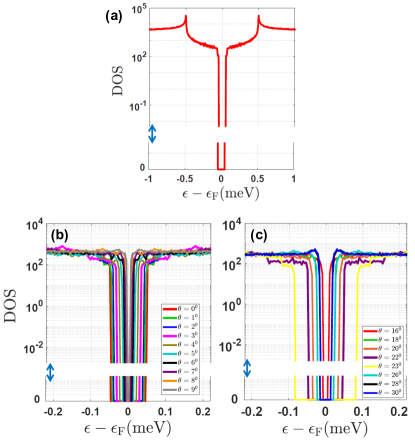
Using tunneling experiments Steinberg et al. (2015); Dvir et al. (2018b) it is possible to obtain the density of states, DOS, of van der Waals systems like graphene-. From the DOS it is then straightforward to extract the value of the induced superconducting gap. Figure 12 (a) shows the total DOS as a function of energy on a linear-log scale. We observe the coherence peaks corresponding to the ’s superconducting gap. Below such coherence peaks the DOS remains finite, because of the graphene’s states, until the energy is equal to . When the energy is equal to the DOS rapidly goes to zero given that at that energy also the graphene’s states become gapped. By analyzing the DOS at small energies we can find how it depends on the twist angle, as shown in Fig. 12 (b), and (c). Figure 12 (b) shows the low energy DOS for several values of close to zero, i.e., for the case when is close to , and Figure 12 (b) shows it for several values of close to , i.e., for the case when the is close to point of ’s extended BZ.
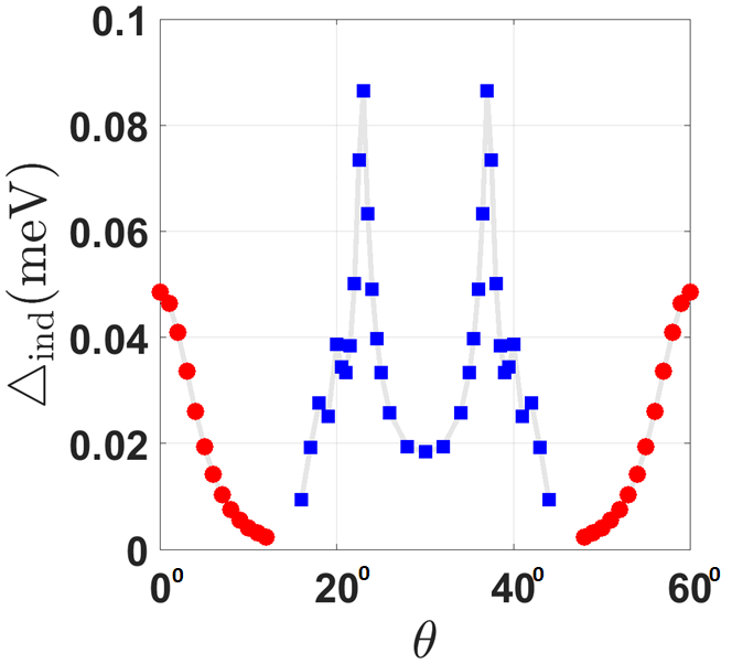
From results like the ones showed in Figs. 12 (b), (c), we can extract the size of the induced superconducting gap and in particular its dependence on the twist angle, Fig. 13. We see that has a fairly sharp peak for (we used a resolution) where it reaches the value of 0.087 meV. This is due to the fact that for there is a very strong overlap of the graphene’s and Fermi surfaces. rapidly decrease as deviates from and becomes an order of magnitude smaller when . has a lower and broader peak for , for wich =0.05 meV, i.e., for the situation in which the graphene’s FS has the maximum overlap with the pockets. As increases from zero smoothly decreases and becomes negligible for . Due to the symmetry of the system the behavior of has a “mirror” symmetry around and is periodic with period equal to , as exemplified by Fig. 13. We notice that the range of values of for which is not vanishingly small is larger than what we can infer by simply looking at the overlaps of the graphene’s and ’s FSs, Fig. 2. The reason is that for finite graphene’s and ’s states that are within the energy window can still hybridize resulting in a nonzero .
Figure 13 shows that in a graphene- structure the superconducting gap can be strongly tuned by varying the twist angle and that, counterintuitively, the maximum induced gap is achieved for a value of for which the graphene’s FS overlaps with the pocket of in the second BZ.
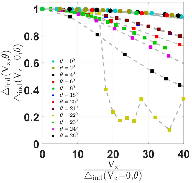
Due to the strong spin-orbit coupling in the in plane critical field is much larger than the field corresponding to the Pauli paramagnetic limit. Due to the fact that SOC is also induced into the graphene layer via proximity effect we find that also for graphene- heterostructures the in plane upper critical field is much larger than the Pauli paramagnetic limit. This is shown in Fig. 14 in which we plot the evolution of in the presence of a Zeeman term both for values of corresponding to the case when the graphene’s FS overlaps ’s pockets (solid lines and circles), and for values of corresponding to the case when the graphene’s FS overlaps ’s pocket (dashed lines and squares). We see that in both cases remains finite for as large as 40 times the induced gap of the system at zero magnetic field. However, it is also evident that the suppression of due to the magnetic field is weaker, and almost independent of , for the case when graphene’s FS overlaps ’s pockets. This is a consequence of the fact that in the bands’ spin splitting due to SOC is much stronger for the pockets than for the pocket.
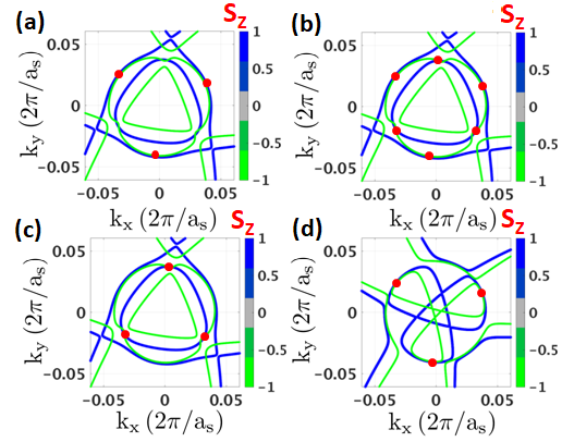
From Fig. 14 we notice that for the dependence of on the Zeeman term deviates from the dependence that we find for the other values of : suddenly decreases when , and it exhibits oscillations for larger values of . The reason is that for this value of there are several points in momentum space for which the induced gap is close to the minimum value and, as shown in Figs. 15 (a)-(c), as increases the point, , in momentum space where the induced gap is minimum moves. This is in contrast to what happens for other value of , for which the gap is minimum always around the same points in space, Figs. 15 (d), regardless of the value of . This implies, for , depending on the value of the minimum gap will be located at points with significantly different amount of SOC-induced spin splitting of the original FSs, and therefore different robustness against an in-plane magnetic field.
IV Conclusions
In conclusion, we have shown that, despite the large lattice mismatch between graphene’s and monolayer ’s lattice constants, in graphene- heterostructures graphene exhibit a significant proximity-induced superconducting gap for a large range of stacking configurations. This is due to the fact that has large FS pockets that overlap with the FS of graphene for most twist angles. Using ab-initio calculations we have obtained the amount of charge transfer between graphene and and estimated the strength of the interlayer tunneling. We have then obtained a continuum model to describe the low energy electronic structure valid in the limit of small interlayer tunneling, condition that the ab-initio results show is satisfied. The continuum model takes into account both the presence of SOC and superconducting pairing in and the fact that, depending on the twist angle, graphene’s FS overlaps either with ’s FS around the point or the point. Using this model, and the value of the parameters from ab-initio calculations, we find that, assuming conservatively the gap in monolayer to be equal to 0.5 mev, and the graphene- tunneling to be 20 meV, the maximum induced superconducting gap in graphene is meV, obtained for a situation when the graphene FS has maximum overlap the ’s FS around the point. We have shown that the superconducting gap induced into the graphene layer is very robust to external in plane magnetic fields: the superconducting gap remains finite for values of the Zeeman term more than 40 times larger then the value of the induced gap in the absence of magnetic fields. In addition, we have shown that such robustness strongly depends on the twist angle in the sense that if is such that the graphene’s FS overlaps with the pockets around the points the induced gap is much more robust to an external in-plane magnetic field than if is such that the graphene’s FS overlaps with the pocket around the pocket. This is a consequence of the fact that the spin-splitting of the bands due to SOC is much stronger at the point than at the point.
The strong dependence on the external magnetic fields of the superconducting gap induced into the graphene layer is a reflection of the fact that graphene can be used, by simply varying the twist angle, as a momentum-selective probe of the electronic structure, and properties, of the substrate. We can therefore envision that tunneling experiments on graphene-based heterostructures could provide very useful, momentum selective, information on the gap structure of systems with more complex gap profiles.
Considering the similarities between the Fermi surface structure of monolayer and other transition metal dichalcogenides our results are relevant also to other graphene-TMDs heterostructures. This also applies to the case in which, instead of a monolayer, a few atomic layers TMD is used. Our results suggests that in general, for a large range of stacking configurations, the graphene and TMD states, despite the large lattice mismatch, are expected to hybridize and, when the TMD is superconducting, induce a significant superconducting gap into the graphene layer. It would be interesting to study how such proximity affect can affect the ground state of twisted-bilayer graphene systems Lu et al. (2016); Cao et al. (2018a, b); Yankowitz et al. (2019); Huang et al. (2018).
V Acknowledgments
We thank Eric Walters for helpful discussions. This work is supported by BSF Grant 2016320. YSG and ER acknowledge support from NSF CAREER grant DMR-1350663. HS is supported by European Research Council Starting Grant (No. 637298, TUNNEL). ER also thanks ONR and ARO for support. The numerical calculations have been performed on computing facilities at William & Mary which were provided by contributions from the NSF, the Commonwealth of Virginia Equipment Trust Fund, and ONR.
References
- Ramasubramaniam (2012) A. Ramasubramaniam, Phys. Rev. B 86, 115409 (2012).
- Latzke et al. (2015) D. W. Latzke, W. Zhang, A. Suslu, T.-R. Chang, H. Lin, H.-T. Jeng, S. Tongay, J. Wu, A. Bansil, and A. Lanzara, Phys. Rev. B 91, 235202 (2015).
- Cazalilla et al. (2014) M. A. Cazalilla, H. Ochoa, and F. Guinea, Phys. Rev. Lett. 113, 077201 (2014).
- Wang et al. (2012) Q. H. Wang, K. Kalantar-Zadeh, A. Kis, J. N. Coleman, and M. S. Strano, Nature Nanotechnology 7, 699 (2012).
- Wang et al. (2015) Z. Wang, D. Ki, H. Chen, H. Berger, A. H. MacDonald, and A. F. Morpurgo, Nature Communications 6 (2015), 10.1038/ncomms9339.
- Gmitra et al. (2016) M. Gmitra, D. Kochan, P. Högl, and J. Fabian, Phys. Rev. B 93, 155104 (2016).
- Duerloo et al. (2014) K.-A. N. Duerloo, Y. Li, and E. J. Reed, Nature Communications 5 (2014), 10.1038/ncomms5214.
- Ugeda et al. (2015) M. M. Ugeda, A. J. Bradley, Y. Zhang, S. Onishi, Y. Chen, W. Ruan, C. Ojeda-Aristizabal, H. Ryu, M. T. Edmonds, and H.-Z. e. a. Tsai, Nature Physics 12, 92 (2015).
- Xi et al. (2015a) X. Xi, Z. Wang, W. Zhao, J.-H. Park, K. T. Law, H. Berger, L. Forró, J. Shan, and K. F. Mak, Nature Physics 12, 139 (2015a).
- Xi et al. (2015b) X. Xi, L. Zhao, Z. Wang, H. Berger, L. Forró, J. Shan, and K. F. Mak, Nature Nanotechnology 10, 765 (2015b).
- Xu et al. (2014) X. Xu, W. Yao, D. Xiao, and T. F. Heinz, Nature Physics 10, 343 (2014).
- Böker et al. (2001) T. Böker, R. Severin, A. Müller, C. Janowitz, R. Manzke, D. Voß, P. Krüger, A. Mazur, and J. Pollmann, Phys. Rev. B 64, 235305 (2001).
- Ding et al. (2011) Y. Ding, Y. Wang, J. Ni, L. Shi, S. Shi, and W. Tang, Physica B: Condensed Matter 406, 2254 (2011).
- Mak et al. (2010) K. F. Mak, C. Lee, J. Hone, J. Shan, and T. F. Heinz, Phys. Rev. Lett. 105, 136805 (2010).
- Dvir et al. (2018a) T. Dvir, F. Massee, L. Attias, M. Khodas, M. Aprili, C. H. L. Quay, and H. Steinberg, Nature Communications 9 (2018a), 10.1038/s41467-018-03000-w.
- Lu et al. (2015) J. M. Lu, O. Zheliuk, I. Leermakers, N. F. Q. Yuan, U. Zeitler, K. T. Law, and J. T. Ye, Science 350, 1353 (2015).
- Saito et al. (2015) Y. Saito, Y. Nakamura, M. S. Bahramy, Y. Kohama, J. Ye, Y. Kasahara, Y. Nakagawa, M. Onga, M. Tokunaga, and T. e. a. Nojima, Nature Physics 12, 144 (2015).
- de la Barrera et al. (2018) S. C. de la Barrera, M. R. Sinko, D. P. Gopalan, N. Sivadas, K. L. Seyler, K. Watanabe, T. Taniguchi, A. W. Tsen, X. Xu, and D. e. a. Xiao, Nature Communications 9 (2018), 10.1038/s41467-018-03888-4.
- Dean et al. (2010) C. R. Dean, A. F. Young, I. Meric, C. Lee., L. Wang, S. Sorgenfrei, K. Watanabe, T. Taniguchi, P. Kim, K. L. Shepard, and J. Hone, Nature Nanotechnology 5, 726 (2010).
- Geim and Grigorieva (2013) A. K. Geim and I. V. Grigorieva, Nature 499, 419 (2013).
- Kou et al. (2013) L. Kou, B. Yan, F. Hu, S.-C. Wu, T. O. Wehling, C. Felser, C. Chen, and T. Frauenheim, Nano Letters 13, 6251 (2013), https://doi.org/10.1021/nl4037214 .
- Zhang et al. (2016) L. Zhang, Y. Yan, H.-C. Wu, D. Yu, and Z.-M. Liao, ACS Nano 10, 3816 (2016), pMID: 26930548, https://doi.org/10.1021/acsnano.6b00659 .
- Zhang et al. (2014) J. Zhang, C. Triola, and E. Rossi, Phys. Rev. Lett. 112, 096802 (2014).
- Zalic et al. (2017) A. Zalic, T. Dvir, and H. Steinberg, Physical Review B 96, 1 (2017).
- Rodriguez-Vega et al. (2017) M. Rodriguez-Vega, G. Schwiete, J. Sinova, and E. Rossi, Phys. Rev. B 96, 235419 (2017).
- Novoselov et al. (2005) K. S. Novoselov, A. K. Geim, S. V. Morozov, D. Jiang, M. I. Katsnelson, I. V. Grigorieva, S. V. Dubonos, and A. A. Firsov, Nature 438, 197 (2005).
- Castro Neto et al. (2009) A. H. Castro Neto, F. Guinea, N. M. R. Peres, K. S. Novoselov, and A. K. Geim, Rev. Mod. Phys. 81, 109 (2009).
- Rossi et al. (2009) E. Rossi, S. Adam, and S. D. Sarma, Phys. Rev. B 79, 245423 (2009).
- Das Sarma et al. (2011) S. Das Sarma, S. Adam, E. H. Hwang, and E. Rossi, Rev. Mod. Phys. 83, 407 (2011).
- Rodriguez-Vega et al. (2014) M. Rodriguez-Vega, J. Fischer, S. Das Sarma, and E. Rossi, Phys. Rev. B 90, 035406 (2014).
- Khestanova et al. (2018) E. Khestanova, J. Birkbeck, M. Zhu, Y. Cao, G. L. Yu, D. Ghazaryan, J. Yin, H. Berger, L. Forró, T. Taniguchi, K. Watanabe, R. V. Gorbachev, A. Mishchenko, A. K. Geim, and I. V. Grigorieva, Nano Letters 18, 2623 (2018).
- Leroux et al. (2012) M. Leroux, P. Rodière, L. Cario, and T. Klein, Physica B: Condensed Matter 407, 1813 (2012), proceedings of the International Workshop on Electronic Crystals (ECRYS-2011).
- Kačmarčík et al. (2010) J. Kačmarčík, Z. Pribulová, C. Marcenat, T. Klein, P. Rodière, L. Cario, and P. Samuely, Phys. Rev. B 82, 014518 (2010).
- Navarro-Moratalla et al. (2016) E. Navarro-Moratalla, J. O. Island, S. Mañas-Valero, E. Pinilla-Cienfuegos, A. Castellanos-Gomez, J. Quereda, G. Rubio-Bollinger, L. Chirolli, J. A. Silva-Guillén, and N. e. a. Agraït, Nature Communications 7 (2016), 10.1038/ncomms11043.
- Giannozzi et al. (2009) P. Giannozzi, S. Baroni, N. Bonini, M. Calandra, R. Car, C. Cavazzoni, D. Ceresoli, G. L. Chiarotti, M. Cococcioni, I. Dabo, A. Dal Corso, S. de Gironcoli, S. Fabris, G. Fratesi, R. Gebauer, U. Gerstmann, C. Gougoussis, A. Kokalj, M. Lazzeri, L. Martin-Samos, N. Marzari, F. Mauri, R. Mazzarello, S. Paolini, A. Pasquarello, L. Paulatto, C. Sbraccia, S. Scandolo, G. Sclauzero, A. P. Seitsonen, A. Smogunov, P. Umari, and R. M. Wentzcovitch, Journal of Physics: Condensed Matter 21, 395502 (19pp) (2009).
- Giannozzi et al. (2017) P. Giannozzi, O. Andreussi, T. Brumme, O. Bunau, M. B. Nardelli, M. Calandra, R. Car, C. Cavazzoni, D. Ceresoli, M. Cococcioni, N. Colonna, I. Carnimeo, A. D. Corso, S. de Gironcoli, P. Delugas, R. A. D. Jr, A. Ferretti, A. Floris, G. Fratesi, G. Fugallo, R. Gebauer, U. Gerstmann, F. Giustino, T. Gorni, J. Jia, M. Kawamura, H.-Y. Ko, A. Kokalj, E. Küçükbenli, M. Lazzeri, M. Marsili, N. Marzari, F. Mauri, N. L. Nguyen, H.-V. Nguyen, A. O. de-la Roza, L. Paulatto, S. Poncé, D. Rocca, R. Sabatini, B. Santra, M. Schlipf, A. P. Seitsonen, A. Smogunov, I. Timrov, T. Thonhauser, P. Umari, N. Vast, X. Wu, and S. Baroni, Journal of Physics: Condensed Matter 29, 465901 (2017).
- Perdew et al. (1996) J. P. Perdew, K. Burke, and M. Ernzerhof, Phys. Rev. Lett. 77, 3865 (1996).
- Mele (2010) E. J. Mele, Phys. Rev. B 81, 161405 (2010).
- Mele (2012) E. J. Mele, Journal of Physics D: Applied Physics 45, 154004 (2012).
- Bistritzer and MacDonald (2011) R. Bistritzer and A. H. MacDonald, Proceedings of the National Academy of Sciences 108, 12233 (2011), http://www.pnas.org/content/108/30/12233.full.pdf .
- Lopes dos Santos et al. (2007) J. Lopes dos Santos, N. Peres, and A. Castro Neto, Phys. Rev. Lett. 99, 256802 (2007).
- Steinberg et al. (2015) H. Steinberg, L. A. Orona, V. Fatemi, J. D. Sanchez-Yamagishi, K. Watanabe, T. Taniguchi, and P. Jarillo-Herrero, Phys. Rev. B 92, 241409 (2015).
- Dvir et al. (2018b) T. Dvir, M. Aprili, C. H. L. Quay, and H. Steinberg, Nano Letters 18, 7845 (2018b), pMID: 30475631.
- Lu et al. (2016) C.-P. Lu, M. Rodriguez-Vega, G. Li, A. Luican-Mayer, K. Watanabe, T. Taniguchi, E. Rossi, and E. Y. Andrei, Proceedings of the National Academy of Sciences 113, 6623 (2016).
- Cao et al. (2018a) Y. Cao, V. Fatemi, S. Fang, K. Watanabe, T. Taniguchi, E. Kaxiras, and P. Jarillo-Herrero, Nature 556, 43 (2018a).
- Cao et al. (2018b) Y. Cao, V. Fatemi, A. Demir, S. Fang, S. L. Tomarken, J. Y. Luo, J. D. Sanchez-Yamagishi, K. Watanabe, T. Taniguchi, E. Kaxiras, R. C. Ashoori, and P. Jarillo-Herrero, Nature 556, 80 (2018b).
- Yankowitz et al. (2019) M. Yankowitz, S. Chen, H. Polshyn, Y. Zhang, K. Watanabe, T. Taniguchi, D. Graf, A. F. Young, and C. R. Dean, Science (2019), 10.1126/science.aav1910.
- Huang et al. (2018) S. Huang, K. Kim, D. K. Efimkin, T. Lovorn, T. Taniguchi, K. Watanabe, A. H. MacDonald, E. Tutuc, and B. J. LeRoy, Phys. Rev. Lett. 121, 037702 (2018).