Uniaxial Strain Induced Topological Phase Transition in Bismuth-Tellurohalide–Graphene Heterostructures
We explore the electronic structure and topological phase diagram of heterostructures
formed of graphene and ternary bismuth tellurohalide layers.
We show that mechanical strain inherently present in fabricated samples could
induce a topological phase transition in single-sided heterostructures,
turning the sample into a novel experimental realisation of a time reversal
invariant topological insulator. We construct an effective tight binding
description for low energy excitations and fit the model’s parameters to
ab initio band structures. We propose a simple approach for predicting
phase boundaries as a function of mechanical distortions and hence gain a
deeper understanding on how the topological phase in the considered system may
be engineered.
1 Introduction
In quantum confined nanostructures the electron-spin dephasing time can reach the order of microseconds, 1, 2, 3 providing an exceptional venue for information processing and information transmission, such as spin-based devices for conventional computers or quantum computing.4, 5, 6, 7 A key difference between spintronic devices and conventional electronics is the controllable manipulation of the spin degree of freedom of charge carriers. Manipulating spins without an external magnetic field is necessary for several technological applications.8 Strong spin-orbit coupling (SOC) in layered two-dimensional (2D) structures potentially leads to band inversion driving the system through a topological phase transition.9, 10, 11. The created novel quantum phase hosts topologically protected edge states whose spin is locked to their propagation direction.12 These spin-momentum locked robust edge states allow for manipulation of the electron spin, hence they have potential as architectural components in a future quantum information processing device.13, 14, 15, 16
Since its first isolation, graphene emerged as an ideal template material for revolutionary applications.17 Although graphene proved to be an electronic conductor with outstanding mechanical properties, the SOC is inherently weak in it due to the small atomic weight of carbon atoms.18, 19 Several theoretical proposals have been made to overcome this limitation for example with introducing curvature in the graphene sheet or by means of adatoms.20, 21 From an engineering point of view, hybrid 2D heterostructures, due to already existing and well understood fabrication procedures, seem a more practical approach for introducing a host of exotic features in graphene samples.22 This method has the potential to introduce a considerably large SOC in the graphene layer of the graphene based devices utilise layered materials with a strong spin-orbit interaction.
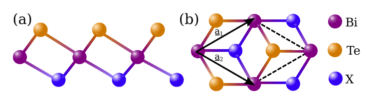
Ternary bismuth tellurohalides are a new class of polar crystals with a layered structure represented by BiTeX .23 The key constituent of these compounds is Bi, which is a heavy element and has a strong atomic SOC. Its triangular lattice layer is stacked between a Te and a halogen atom layer, see Figure 1. The already large intrinsic SOC in Bi and the structural asymmetry combined with a large in-plane gradient of the crystal field in this lattice results in giant Rashba spin-splitting semiconductors.24, 25, 26, 27, 28 Among these BiTeI stands out with the strongest SOC.29 It was also shown that centrosymmetric thin films composed from topologically trivial BiTeI trilayers are quantum spin Hall insulators and properly stacked compounds of BiTeX results in topological insulating phase. 30, 31 Recently the first experimental isolation and characterisation of a single layer of BiTeI was reported by Fülöp et al. using a novel exfoliation technique.32 Albeit the band gap increased, the basic characteristics of bulk BiTeI is preserved, hence this material can be used as a strong SOC inducing component in graphene based heterostructures, as it was theoretically studied in previous works.33, 34
In this manuscript, we give an account of a detailed theoretical investigation of heterostructures consisting of graphene and BiTeX layered van der Waals systems. Based on first principle calculations we distilled an effective model in order to understand the emerging topological phase in the studied structures and explored the phase diagram of the systems as a function of mechanical distortions. We identify single-sided BiTeX-graphene heterostructures as promising candidates for engineering mechanically controllable topological phases. Although mechanical control of topological properties has already been demonstrated, our proposal is the first to point out that uniaxial in-plane strain can also be used for engineering topological phases. 35
2 First principles results
2.1 Electronic structure of BiTeX-graphene hybrid systems
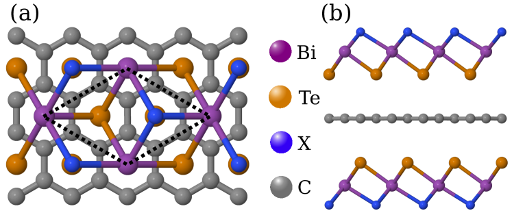
The crystal structure of BiTeX is characterised by similar experimental in-plane lattice constants nm, nm, nm for respectively.36 As these values are approximately times larger than the lattice constant of graphene (nm), it is possible to find a commensurate supercell by the 30∘ rotation of the graphene layer. This supercell is depicted in Figure 2(a) consisting of six carbon atoms, one bismuth, one tellurium and one halogen atom. Note that this choice leads to a strain not larger than in the BiTeX lattice. This mismatch may alters the band structure of the BiTeX layer but it does not influence our main conclusions. Furthermore, we only consider the so called hollow configuration, that is when the adjacent atom of the BiTeX layer (i.e., Te or X) is positioned above the centre of a hexagon of carbon atoms in the graphene layer, as it was shown previously that this horizontal configuration is the most stable.33
| Structure | nm | ||
|---|---|---|---|
| BiTeI - C | 0.344 | 0 | |
| BiTeI - C | 0.342 | metallic | N.A. |
| BiTeI - C [I faced] | 0.335 | metallic | N.A. |
| BiTeI - C - BiTeI | 0.345 | 44 | 1 |
| BiTeI - C - BiTeI | 0.346 | metallic | N.A. |
| BiTeI - C - BiTeI | 0.344 | metallic | N.A. |
| BiTeCl - C | 0.346 | 0 | |
| BiTeCl - C | 0.344 | metallic | N.A. |
| BiTeCl - C [Cl faced] | 0.300 | metallic | N.A. |
| BiTeCl - C - BiTeCl | 0.346 | 41 | 1 |
| BiTeCl - C - BiTeCl | 0.344 | metallic | N.A. |
| BiTeCl - C - BiTeCl | 0.353 | metallic | N.A. |
| BiTeBr - C | 0.344 | 0 | |
| BiTeBr - C | 0.339 | metallic | N.A. |
| BiTeBr - C [Br faced] | 0.309 | metallic | N.A. |
| BiTeBr - C - BiTeBr | 0.346 | 42 | 1 |
| BiTeBr - C - BiTeBr | 0.345 | metallic | N.A. |
| BiTeBr - C - BiTeBr | 0.344 | metallic | N.A. |
| BiTeI - C - BiTeCl | 0.344 | 42 | 1 |
| BiTeI - C - BiTeBr | 0.347 | 44 | 1 |
| BiTeBr - C - BiTeCl | 0.344 | 43 | 1 |
We compared various combinations of the two constituents of the investigated heterostructure, BiTeX layers and graphene. First we studied single-sided setups, comprising of a single layer of graphene and one or two layers of BiTeX, taking both Te and X faced alignments into account. We also dealt with two sided "sandwich" structures, where the graphene sheet is surrounded by one or two layers of BiTeX from both sides. In the investigated sandwich structures Te layers were always facing graphene. The initial geometry of all considered configurations were fully relaxed, allowing also for change of the in-plane lattice parameter. We found however that in all cases the optimal geometry yielded the in-plane lattice constant of graphene, as expected due to the larger stiffness of graphene.37 The obtained optimal layer distances, bulk band gap of electronic states (if any) and topological invariant (for insulators) are compiled in Table 1.
The layer distance between BiTeX and graphene was found to be around Å for all considered arrangements, thus one can safely conclude that the interlayer interaction in these systems is of van der Waals type. For the single-sided Br or Cl faced BiTeX graphene configurations the interlayer distance was found significantly reduced compared to other cases. This tendency correlates well to the widely accepted, experimentally extracted van der Waals radii, which are also definitely lower for Br and Cl atoms compared to Te and I atoms.38, 39
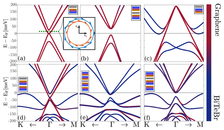
In Figure 3 we present the calculated electronic band structures for all considered BiTeBr-graphene structures around the Fermi energy. colouring of the bands corresponds to the orbital weights of the constituent layers, carbon orbitals are shaded red while states localised to BiTeBr layers are depicted by blueish colours, a purple hue signifies a strongly hybridised state. Depending on the number of BiTeBr layers and their relative alignment the studied systems show several distinct features.
Figure 3 (a) and (b) depict single-sided and sandwich structures of Te faced monolayer BiTeBr-graphene arrangements for which cases the low energy spectrum is dominated by quasiparticle contributions localised to the carbon atoms, reminiscent of the Dirac cones of graphene. In Figure 3(a) the inset shows a schematic representation of the spin texture of the two first conduction bands at a constant energy contour at 20 meV. We note, that in the inset, for clarity, the small but finite spin-splitting of the lowermost conduction band is artificially enlarged in -space. The arrows representing the direction of the spin expected value in the - plane. The direction of the arrows are the same in the inner and the outer circle indicating a spin helicity in the graphene Dirac bands. The spin polarization also demonstrates the presence of the out-of-plane spin component. This finding is in good agreement with the observation of Eremeev et al., where the authors examined a similar setup of BiTeCl and graphene.40
In these two cases the Dirac point is auspiciously tuned to the gap of the BiTeBr monolayer bands. Since these structures are primarily characterised by graphene like bands, they might be understood in terms of a simplified model where the orbitals of carbon atoms are subject to an induced spin-orbit coupling (see section 3). The main difference between the single-sided and sandwich structures is that, while in the sandwich structure a sizable direct gap of is present at the point, in the single-sided system the calculation yields a considerably smaller gap of about . We also extracted the topological invariant by calculating the flow of Wannier centres in the half of the Brillouin zone 41, 42 based on the ab initio Hamiltonian (for details see section 4). The topological classification of the sandwich structure confirms the findings of Kou and coworkers namely that the gap in sandwich structures is topological.33 On the other hand based on our calculations the small gap in the single-sided system is trivial.
In the other investigated scenarios depicted in Figure 3 (c)-(f), in contrast to the Te faced monolayer BiTeBr-graphene arrangements, the image of the Dirac point is either considerably shifted away from the Fermi level or it is masked by states originating from BiTeBr, thus a strong mixing of BiTeBr and carbon bands occurs, resulting in metallic band structures. Similar trends can be identified in other arrangements, independently from the type of halogen atom considered (cf. Table 1).
In the remainder of the manuscript we shall focus on the setups where the low energy electronic structure is dominated by the orbitals of graphene. Therefore, we shall only consider the Te faced sandwich and the monolayer BiTeX-graphene arrangements.
2.2 Effect of mechanical distortions
Previously, we presented results obtained for relaxed geometries. Manufactured devices are commonly subject to mechanical distortions which in turn can have a non-negligible impact on the electronic properties of the system. Recently considerable experimental effort has been made to make use of strain fields to control electronic and optical properties of novel heterostructures. 43, 44, 45, 46 Inspired by these advances, we investigate below how the electronic states and their topological character is influenced in Te faced single-sided BiTeBr-graphene heterostructure as the sample is subjected to in-plane uniaxial strain combined with stress perpendicular to the device.
We model in-plane uniaxial strain in our ab initio calculations by stretching the in-plane unit cell vectors along a carbon–carbon bond, and allowing the atomic positions relax in the constrained unit cell. On the other hand out-of-plane strain is simulated by reducing the distance between graphene and the BiTeX layer, without relaxation of the atomic positions.
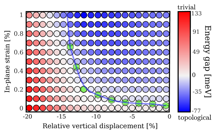
We calculated the evolution of the size of the band gap and the topological index as both in-plane and out-of-plain strain was varied. The corresponding phase diagram is shown on Figure 4. The sign of the band gap indicates the topological invariant, it is negative if the system is topological and positive otherwise.
Based on the presented results we conclude that both type of mechanical distortions have a striking effect on the band gap, however they favour different topological phases. Out-of-plane strain widens the initially present trivial band gap, while in-plane strain drives the system into the topological phase. We only present results for BiTeBr further calculations show that BiTeCl behaves qualitatively in the same fashion. BiTeI turns metallic instead of a trivial insulator due to some non graphene bands reaching the Fermi level as pressure is increased.
We note that the largest out-of plane strain we applied would correspond to a nominal pressure of GPa, which we estimated as the energy derivation per unit area over the reduced distance. The mechanical stresses considered in our calculations can thus be routinely achieved in nowadays experimental setups.47, 48, 49, 50, 51, 52, 53, 54
3 Low energy description
3.1 A model Hamiltonian
In the previous section, based on first principles calculations, we identified two arrangements from all the considered structures where electronic states close to the Fermi energy are dominated by the orbitals of carbon atoms. These two setups, the Te faced single-sided BiTeX-graphene heterostructure and the sandwich system, are depicted in the insets of Figure 3 (a) and (b). In this section we propose an effective model, based on the tight binding (TB) description of graphene, where due to the presence of BiTeX layers an appropriately patterned SOC emerges. With the help of the introduced model we gain a deeper insight into the mechanisms responsible for the emergence of the topological phase witnessed before. Our effective description of the heterostructure is cast in a form that is digestible for theoretical approaches calculating electron, thermal and spin transport properties of samples on experimentally relevant scales.55, 56
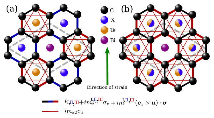
Respecting the symmetries of the system studied in the first principles calculations, we introduce a model with only a minimal number of parameters. Beyond the usual hopping integrals , we assume spin-orbit interaction compatible with time reversal symmetry on nearest neighbour carbon-carbon bonds as , where is a real vector, is the vector of Pauli matrices. We also include second nearest neighbour out-of-plane spin-orbit interaction as it was previously proposed by Kane and Mele to germinate a topological phase transition in graphene like systems.57 The studied systems are invariant under the symmetries of the point group. The in-plane component of the vector on each bond is restricted by this symmetry and points perpendicular to the bonds 58. After taking into account all the symmetries of the system our simplified model is depicted on Figure 5a. Thus we introduce three different nearest neighbour hopping integrals , three in-plane and three out-of-plane spin-orbit interaction magnitudes and a second-nearest neighbour out-of-plane spin-orbit interaction strength .
In the absence of the BiTeX layers graphene also possesses inversion symmetry with an inversion centre in the middle of each hexagon. This symmetry is altered in the case of the sandwich arrangement in such a way that only hexagon centres aligned with Bi atoms remain inversion centres. In this case inversion symmetry forbids SOC on first nearest-neighbour bonds (denoted by thick black lines in Figure 5b), while it connects the hopping and SOC magnitudes along bonds that was marked by red and blue thick lines in Figure 5a), that is the two hoppings must be equal in the case of inversion symmetry. This yields , and while . We now make some further assumptions regarding the actual investigated system. Since the interaction between BiTeX and graphene is van der Waals type and the Bi atoms are further away from the graphene sheet as the Te atoms we neglect the second nearest neighbour SOC on the hexagonal plaquettes encircling Bi atoms.
Breaking inversion symmetry by separating one of the BiTeX layer from the sandwich structure results in a Te faced single-sided geometry. In this case nearest neighbour SOC is allowed on thick black bonds, and blue and red bonds are no longer connected. Consistently with our previous approach we neglect second nearest neighbour SOC on the plaquettes encircling X atoms since they are even further from the graphene sheet as Bi. Therefore the single-sided setup is characterised by 10 different parameters, the hopping amplitudes , first nearest neighbour in-plane SOC and out-of plane SOC with and the only second nearest neighbour SOC in hexagons surrounding Te atoms. In both cases the red thin lines denote the considered second nearest neighbour SOC interactions in Figure 5.
We thus constructed the real space Hamiltonian as:
| (1) |
The sum in and goes over all unit cells in the crystal, while indicate one of the six atoms in a given unit cell. Annihilation (creation) operators for an electron in unit cell on site are denoted by , is a unit vector pointing in the direction, is the vector that points from site in unit cell to site in unit cell and is the identity operator.
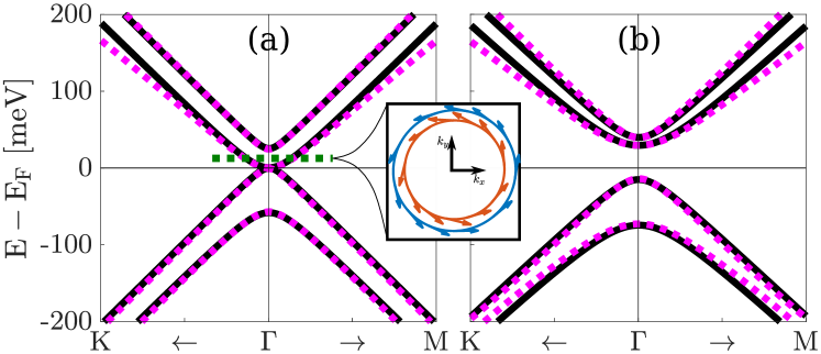
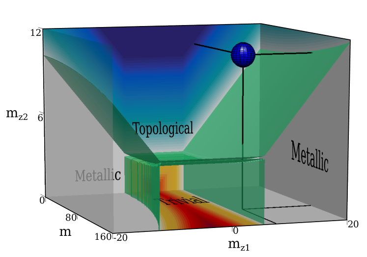
The fitted and first principles band structure are depicted together for both the single-sided and sandwich structures in Figure 6. In the following we map the topological character of the introduced two models. Tracking again the evolution of Wannier centres yields the topological invariant for the proposed effective Hamiltonian.41, 42 First we investigate the inversion symmetric sandwich setup, and focus on the parameters responsible for spin-orbit interaction, , and while fixing the two hopping terms to and . The phase diagram in Figure 7 shows two topologically distinct insulating phases and a metallic phase. We observe that without SOC but in the presence of a hopping mismatch the model is a trivial Kekulé patterned band insulator as it was studied in clean graphene under appropriate biaxial strain.59 The first nearest neighbour out-of plane SOC drives the system towards a gapless metallic phase, while the second nearest neighbour SOC promotes the topological insulator phase, large eventually drives the system into the trivial insulator phase as it also does in more simple models.57 A blue sphere denotes the parameter configuration that represent the fit to the ab initio result for the sandwich configuration.
| Structure | ||||||||||
|---|---|---|---|---|---|---|---|---|---|---|
| BiTeI - C | 2400 | 2580 | 2369 | -0.232 | -403.1 | -396.3 | 0.010 | 28.97 | -3.797 | -11.80 |
| BiTeBr - C | 2379 | 2382 | 2376 | -0.586 | 147.3 | 188.9 | 3.227 | 4.434 | 7.533 | -5.722 |
| BiTeCl - C | 2359 | 2369 | 2370 | 0.568 | -29.95 | -38.77 | 0.061 | 20.89 | -5.685 | -11.59 |
| BiTeI - C - BiTeI | 2268 | 2274 | 0 | 146.9 | 0 | 7.304 | 11.15 | |||
| BiTeBr - C - BiTeBr | 2227 | 2210 | 0 | 138.4 | 0 | 11.90 | 10.64 | |||
| BiTeCl - C - BiTeCl | 2251 | 2258 | 0 | 129.8 | 0 | 6.040 | 9.900 | |||
3.2 Understanding the role of mechanical distortions
Turning our attention to the single-sided arrangements our main goal is to understand the phase diagram emerging from the first principles calculations presented in Figure 4 describing a topological phase transition driven by in-plane uniaxial strain and compression perpendicular to the sample. In the absence of in-plane distortions but under out-of-plane strain the system can still be well approximated by the model described in the previous section. Unavoidably, the application of uniaxial deformation breaks symmetry of the system. We included this effect into our model by multiplying all first nearest neighbour hopping and SOC terms in the direction of the uniaxial strain by a common factor .60 In this multiplicative term is the bond length in stress free system, is the bond length in the deformed case and is a dimensionless parameter determined from fitting to ab initio calculations performed on freestanding graphene. This approach is widely used in the literature for describing the effects of mechanical distortions on TB parameters. 60, 61 We note that following common practice bonds not parallel with the distortion were not modified. We also remark that this method is applicable for small to moderate strain values where buckling of the hexagons is negligible. 62
Using this simple model for in-plane distortions we are now equipped for exploring the phase diagram of the effective system. We first fit our symmetric model to ab initio calculations performed for geometries without uniaxial in-plane strain. Introducing strain in these models as described above we calculate the size of the quasi particle gap and the topological invariant. The phase boundary of the TB model is depicted with green hexagons in Figure 4. It shows that for all cases the initially present trivial gap closes and a topological gap opens as one tunes the magnitude of uniaxial strain in the multiplicative factor. As it can be observed in Figure 4. our rudimentary approach for including the strain in the effective model adequately predicts the boundary of the topological phase, even for moderately large compressions, thus justifying its application. One can understand the emerging topological phase transition in the investigated heterostructures as a competition of a trivial gap of Kekulé type and a topological Kane-Mele type.59, 57 Due to time reversal symmetry uniaxial strain displaces the Dirac cones of graphene in the two valleys in the opposite direction. Since Kekulé distortion hybridises the different valleys it is impeded by the strain. At a given finite strain value the topological component thus overpowers the trivial and a system turns into a time reversal invariant topological insulator.
4 Methods
The optimised geometry and ground state Hamiltonian and overlap matrix elements of each structure were self consistently obtained by the SIESTA implementation of density functional theory (DFT)63, 64. SIESTA employs norm-conserving pseudopotentials to account for the core electrons and linear combination of atomic orbitals to construct the valence states. For all cases the considered samples were separated with a minimum of nm thick vacuum in the perpendicular direction. The generalised gradient approximation of the exchange and the correlation functional was used with Perdew-Burke-Ernzerhof parametrisation65 and the pseudopotentials optimised by Rivero et al.66 with a double- polarised basis set and a real-space grid defined with an equivalent energy cutoff of . The Brillouin zone integration was sampled by a Monkhorst-Pack -grid.67 The geometry optimisations were performed until the forces were smaller than nm. The choice of pseudopotentials optimised by Rivero et al. ensures that both the obtained geometrical structures and the electronic band properties are reliable. As a benchmark we validated our method by comparing the electronic properties of the bulk BiTeI with the experimental data. This approach gave us band gap and as Rashba parameter for BiTeI bulk. The corresponding experimental results are and respectively. 29 Relativistic effects, including spin-orbit coupling, were fully taken into account in every performed calculation. 68
The fitting procedure was carried out by applying a constrained least squares minimisation procedure to the difference between the TB and the DFT band energies. As one progresses further in energy away from the Fermi level the assumption that carbon orbital contributions dominate begins to break down, with significant BiTeX orbital contributions at energies around . Therefore we fit the model to only 8 bands in an energy window of . The fit is carried out over 720 points in -space along the high symmetry lines of the Brillouin zone. While the procedure is in principle straightforward, in practice one must take care, in particular with the choice of bands to use for the fitting procedure. On diagonalization the model yields 12 bands. We fit the model to the 4 highest energy occupied and the 4 lowest energy valence bands, as the graphene’s Dirac cones are 8 times degenerate in the gamma point in the case of a supercell. Additionally we took into account the invariant of the system and the spin structure of the 8 fitted bands, that is calculating the expected values of the spin orientations. The fitness of the procedure is presented in the inset figure of Figure 6, which is in good agreement of the DFT results (inset figure of Figure 3).
5 Conclusion
In summary, we explored the rich topological phase diagram of bismuth tellurohalide/graphene heterostructures by means of first principles calculations. Based on our ab initio results we distilled a simple tight binding description for the investigated system capturing all relevant features of the low energy spectra of quasiparticles. We have demonstrated that the topological phase transition due to mechanical distortions in one-sided systems leads to a novel realisation of the time reversal invariant topological insulating phase, thus making these heterostructures potential candidates for quantum technology applications.
Conflicts of interest
There are no conflicts to declare.
Acknowledgements
This work was financially supported by the the Hungarian National Research, Development and Innovation Office (NKFIH) via the National Quantum Technologies Program 2017-1.2.1-NKP-2017-00001; grants no. K112918, K115608, FK124723, K115575 and Flag-ERA iSpinText project NN118996. This work was completed in the ELTE Excellence Program (1783-3/2018/FEKUTSTRAT) supported by the Hungarian Ministry of Human Capacities. LO, JK acknowledge the Bolyai and Bolyai+ program of the Hungarian Academy of Sciences. We acknowledge [NIIF] for awarding us access to resource based in Hungary at Debrecen.
Notes and references
- 1 David D. Awschalom and James M. Kikkawa. Electron Spin and Optical Coherence in Semiconductors. Phys. Today, 52(6):33–38, June 1999.
- 2 J. R. Petta, A. C. Johnson, J. M. Taylor, E. A. Laird, A. Yacoby, M. D. Lukin, C. M. Marcus, M. P. Hanson, and A. C. Gossard. Coherent manipulation of coupled electron spins in semiconductor quantum dots. Science, 309(5744):2180–2184, 2005.
- 3 R. Hanson, L. P. Kouwenhoven, J. R. Petta, S. Tarucha, and L. M. K. Vandersypen. Spins in few-electron quantum dots. Rev. Mod. Phys., 79(4):1217–1265, 2007.
- 4 Guido Burkard, Hans-Andreas Engel, and Daniel Loss. Spintronics and quantum dots for quantum computing and quantum communication. Fortschr. Phys., 48(9):965–986, 2000.
- 5 Michael N Leuenberger and Daniel Loss. Spintronics and quantum computing: switching mechanisms for qubits. Phys. E, 10(1-3):452–457, May 2001.
- 6 Juan M. Clemente-Juan, Eugenio Coronado, and Alejandro Gaita-Ariño. Magnetic polyoxometalates: from molecular magnetism to molecular spintronics and quantum computing. Chem. Soc. Rev., 41(22):7464–7478, 2012.
- 7 Sergey V. Eremeev, Stepan S. Tsirkin, Ilya A. Nechaev, Pedro M. Echenique, and Evgueni V. Chulkov. New generation of two-dimensional spintronic systems realized by coupling of rashba and dirac fermions. Sci. Rep., 5(1):12819, 2015.
- 8 Igor Žutić, Jaroslav Fabian, and S. Das Sarma. Spintronics: Fundamentals and applications. Rev. Mod. Phys., 76(2):323–410, April 2004.
- 9 Chengwang Niu, Patrick M Buhl, Gustav Bihlmayer, Daniel Wortmann, Stefan Blügel, and Yuriy Mokrousov. Two-dimensional topological crystalline insulator phase in quantum wells of trivial insulators. 2D Mater., 3(2):025037, June 2016.
- 10 Yoichi Ando and Liang Fu. Topological crystalline insulators and topological superconductors: From concepts to materials. Annu. Rev. Condens. Matter Phys., 6(1):361–381, 2015.
- 11 Liang Fu. Topological crystalline insulators. Phys. Rev. Lett., 106(10):106802, 2011.
- 12 M. Z. Hasan and C. L. Kane. Colloquium : Topological insulators. Rev. Mod. Phys., 82(4):3045–3067, 2010.
- 13 Michael Freedman, Alexei Kitaev, Michael Larsen, and Zhenghan Wang. Topological quantum computation. Bull. Amer. Math. Soc., 40(1):31–38, 2003.
- 14 A. Yu. Kitaev. Fault-tolerant quantum computation by anyons. Ann. Phys., 303(1):2–30, 2003.
- 15 Chetan Nayak, Steven H. Simon, Ady Stern, Michael Freedman, and Sankar Das Sarma. Non-abelian anyons and topological quantum computation. Rev. Mod. Phys., 80(3):1083–1159, 2008.
- 16 Earl T. Campbell, Barbara M. Terhal, and Christophe Vuillot. Roads towards fault-tolerant universal quantum computation. Nature, 549(7671):172–179, 2017.
- 17 K. S. Novoselov, A. K. Geim, S. V. Morozov, D. Jiang, Y. Zhang, S. V. Dubonos, I. V. Grigorieva, and A. A. Firsov. Electric field effect in atomically thin carbon films. Science, 306(5696):666–669, 2004.
- 18 Nikolaos Tombros, Csaba Jozsa, Mihaita Popinciuc, Harry T. Jonkman, and Bart J. van Wees. Electronic spin transport and spin precession in single graphene layers at room temperature. Nature, 448(7153):571–574, 2007.
- 19 A. H. Castro Neto and F. Guinea. Impurity-induced spin-orbit coupling in graphene. Phys. Rev. Lett., 103(2):026804, 2009.
- 20 Daniel Huertas-Hernando, F. Guinea, and Arne Brataas. Spin-orbit coupling in curved graphene, fullerenes, nanotubes, and nanotube caps. Phys. Rev. B, 74(15):155426, 2006.
- 21 Jayakumar Balakrishnan, Gavin Kok Wai Koon, Manu Jaiswal, A. H. Castro Neto, and Barbaros Özyilmaz. Colossal enhancement of spin–orbit coupling in weakly hydrogenated graphene. Nat. Phys., 9(5):284–287, 2013.
- 22 A. K. Geim and I. V. Grigorieva. Van der Waals heterostructures. Nature, 499(7459):419–425, July 2013.
- 23 M. S. Bahramy, R. Arita, and N. Nagaosa. Origin of giant bulk Rashba splitting: Application to BiTeI. Physical Review B, 84(4):041202, July 2011.
- 24 Christian R. Ast, Jürgen Henk, Arthur Ernst, Luca Moreschini, Mihaela C. Falub, Daniela Pacilé, Patrick Bruno, Klaus Kern, and Marco Grioni. Giant Spin Splitting through Surface Alloying. Phys. Rev. Lett., 98(18):186807, May 2007.
- 25 Lihua Wu, Jiong Yang, Miaofang Chi, Shanyu Wang, Ping Wei, Wenqing Zhang, Lidong Chen, and Jihui Yang. Enhanced thermoelectric performance in cu-intercalated BiTeI by compensation weakening induced mobility improvement. Sci. Rep., 5:14319, 2015.
- 26 M. Sakano, J. Miyawaki, A. Chainani, Y. Takata, T. Sonobe, T. Shimojima, M. Oura, S. Shin, M. S. Bahramy, R. Arita, N. Nagaosa, H. Murakawa, Y. Kaneko, Y. Tokura, and K. Ishizaka. Three-dimensional bulk band dispersion in polar BiTeI with giant rashba-type spin splitting. Phys. Rev. B, 86(8):085204, 2012.
- 27 Christopher John Butler, Hung-Hsiang Yang, Jhen-Yong Hong, Shih-Hao Hsu, Raman Sankar, Chun-I Lu, Hsin-Yu Lu, Kui-Hon Ou Yang, Hung-Wei Shiu, Chia-Hao Chen, Chao-Cheng Kaun, Guo-Jiun Shu, Fang-Cheng Chou, and Minn-Tsong Lin. Mapping polarization induced surface band bending on the rashba semiconductor BiTeI. Nat. Commun., 5(1):4066, 2014.
- 28 Yanpeng Qi, Wujun Shi, Pavel G. Naumov, Nitesh Kumar, Raman Sankar, Walter Schnelle, Chandra Shekhar, Fang-Cheng Chou, Claudia Felser, Binghai Yan, and Sergey A. Medvedev. Topological quantum phase transition and superconductivity induced by pressure in the bismuth tellurohalide BiTeI. Adv. Mater., 29(18):1605965, 2017.
- 29 K. Ishizaka, M. S. Bahramy, H. Murakawa, M. Sakano, T. Shimojima, T. Sonobe, K. Koizumi, S. Shin, H. Miyahara, A. Kimura, K. Miyamoto, T. Okuda, H. Namatame, M. Taniguchi, R. Arita, N. Nagaosa, K. Kobayashi, Y. Murakami, R. Kumai, Y. Kaneko, Y. Onose, and Y. Tokura. Giant Rashba-type spin splitting in bulk BiTeI. Nat. Mater., 10(7):521–526, July 2011.
- 30 I. A. Nechaev, S. V. Eremeev, E. E. Krasovskii, P. M. Echenique, and E. V. Chulkov. Quantum spin hall insulators in centrosymmetric thin films composed from topologically trivial BiTeI trilayers. Scientific Reports, 7(1):43666, 2017.
- 31 S. V. Eremeev, I. A. Nechaev, and E. V. Chulkov. Two- and three-dimensional topological phases in BiTe x compounds. Physical Review B, 96(15):43666, 2017.
- 32 Bálint Fülöp, Zoltán Tajkov, János Pető, Péter Kun, János Koltai, László Oroszlány, Endre Tóvári, Hiroshi Murakawa, Yoshinori Tokura, Sándor Bordács, Levente Tapasztó, and Szabolcs Csonka. Exfoliation of single layer BiTeI flakes. 2D Mater., 5(3):031013, June 2018.
- 33 Liangzhi Kou, Shu-Chun Wu, Claudia Felser, Thomas Frauenheim, Changfeng Chen, and Binghai Yan. Robust 2d Topological Insulators in van der Waals Heterostructures. ACS Nano, 8(10):10448–10454, October 2014.
- 34 Z. Tajkov, D. Visontai, P. Rakyta, L. Oroszlány, and J. Koltai. Transport Properties of Graphene-BiTeI Hybrid Structures. Phys. Status Solidi C, 14(11):1700215, November 2017.
- 35 Yafei Ren, Zhenhua Qiao, and Qian Niu. Topological phases in two-dimensional materials: a review. Reports on Progress in Physics, 79(6):066501, 2016.
- 36 A. V. Shevelkov, E. V. Dikarev, R. V. Shpanchenko, and B. A. Popovkin. Crystal Structures of Bismuth Tellurohalides BiTeX (X = Cl, Br, I) from X-Ray Powder Diffraction Data. J. Solid State Chem., 114(2):379–384, February 1995.
- 37 Changgu Lee, Xiaoding Wei, Jeffrey W. Kysar, and James Hone. Measurement of the elastic properties and intrinsic strength of monolayer graphene. Science, 321(5887):385–388, 2008.
- 38 A. Bondi. van der waals volumes and radii. J. Phys. Chem., 68(3):441–451, 1964.
- 39 R. Scott Rowland and Robin Taylor. Intermolecular nonbonded contact distances in organic crystal structures: Comparison with distances expected from van der waals radii. J. Phys. Chem., 100(18):7384–7391, 1996.
- 40 S. V. Eremeev, I. A. Nechaev, P. M. Echenique, and E. V. Chulkov. Spin-helical dirac states in graphene induced by polar-substrate surfaces with giant spin-orbit interaction: a new platform for spintronics. Scientific Reports, 4:6900, 2014.
- 41 Shinsei Ryu, Andreas Schnyder, Akira Furusaki, and Andreas Ludwig. Topological insulators and superconductors: ten-fold way and dimensional hierarchy. New J. Phys., 12(6):065010, 2010.
- 42 János K. Asbóth, László Oroszlány, and András Pályi. A Short Course on Topological Insulators: Band Structure and Edge States in One and Two Dimensions, volume 909 of Lecture Notes in Physics. Springer International Publishing, BerlinXXX, 1st edition, Z 2016.
- 43 Andres Castellanos-Gomez, Rafael Roldán, Emmanuele Cappelluti, Michele Buscema, Francisco Guinea, Herre S. J. van der Zant, and Gary A. Steele. Local strain engineering in atomically thin mos2. Nano Lett., 13(11):5361–5366, 2013.
- 44 Yuhang Jiang, Jinhai Mao, Junxi Duan, Xinyuan Lai, Kenji Watanabe, Takashi Taniguchi, and Eva Y. Andrei. Visualizing strain-induced pseudomagnetic fields in graphene through an hbn magnifying glass. Nano Lett., 17(5):2839–2843, 2017.
- 45 Javier Martín-Sánchez, Rinaldo Trotta, Antonio Mariscal, Rosalía Serna, Giovanni Piredda, Sandra Stroj, Johannes Edlinger, Christian Schimpf, Johannes Aberl, Thomas Lettner, Johannes Wildmann, Huiying Huang, Xueyong Yuan, Dorian Ziss, Julian Stangl, and Armando Rastelli. Strain-tuning of the optical properties of semiconductor nanomaterials by integration onto piezoelectric actuators. Semicond. Sci. Technol., 33(1):013001, dec 2017.
- 46 Matthias Goldsche, Jens Sonntag, Tymofiy Khodkov, Gerard Jan Verbiest, Sven Reichardt, Christoph Neumann, Taoufiq Ouaj, Nils von den Driesch, Dan Buca, and Christoph Stampfer. Tailoring mechanically tunable strain fields in graphene. Nano Lett., 18(3):1707–1713, 2018. PMID: 29425440.
- 47 Chaoyu Song, Fengren Fan, Ningning Xuan, Shenyang Huang, Guowei Zhang, Chong Wang, Zhengzong Sun, Hua Wu, and Hugen Yan. Largely tunable band structures of few-layer InSe by uniaxial strain. ACS Applied Materials & Interfaces, 10(4):3994–4000, 2018.
- 48 Wen Fan, Xi Zhu, Feng Ke, Yabin Chen, Kaichen Dong, Jie Ji, Bin Chen, Sefaattin Tongay, Joel W. Ager, Kai Liu, Haibin Su, and Junqiao Wu. Vibrational spectrum renormalization by enforced coupling across the van der waals gap between and monolayers. Phys. Rev. B, 92:241408, Dec 2015.
- 49 G. Vecchi, V. Giannini, and J. Gómez Rivas. Surface modes in plasmonic crystals induced by diffractive coupling of nanoantennas. Phys. Rev. B, 80:201401, Nov 2009.
- 50 Annette K. Kleppe, Mónica Amboage, and Andrew P. Jephcoat. New high-pressure van der waals compound kr(h) discovered in the krypton-hydrogen binary system. Sci. Rep., 4:4989, 2014.
- 51 Zhen Hua Ni, Ting Yu, Yun Hao Lu, Ying Ying Wang, Yuan Ping Feng, and Ze Xiang Shen. Uniaxial strain on graphene: Raman spectroscopy study and band-gap opening. ACS Nano, 2(11):2301–2305, 2008.
- 52 Lellis F. Braganza and David L. Worcester. Hydrostatic pressure induces hydrocarbon chain interdigitation in single-component phospholipid bilayers. Biochemistry, 25(9):2591–2596, 1986.
- 53 W. L. Vos, L. W. Finger, R. J. Hemley, J. Z. Hu, H. K. Mao, and J. A. Schouten. A high-pressure van der waals compound in solid nitrogen-helium mixtures. Nature, 358(6381):46, 1992.
- 54 W. Kullmann, J. Geurts, W. Richter, N. Lehner, H. Rauh, U. Steigenberger, G. Eichhorn, and R. Geick. Effect of hydrostatic and uniaxial pressure on structural properties and raman active lattice vibrations in bi2te3. Phys. Status Solidi B, 125(1):131–138, 1984.
- 55 Equus: Eötvös Quantum Transport Utilities, http://eqt.elte.hu/equus/home.
- 56 J Ferrer, C J Lambert, V M García-Suárez, D Zs Manrique, D Visontai, L Oroszlany, R Rodríguez-Ferradás, I Grace, S W D Bailey, K Gillemot, Hatef Sadeghi, and L A Algharagholy. GOLLUM: a next-generation simulation tool for electron, thermal and spin transport. New J. Phys., 16(9):093029, sep 2014.
- 57 C. L. Kane and E. J. Mele. Quantum spin hall effect in graphene. Phys. Rev. Lett., 95:226801, Nov 2005.
- 58 Roland Winkler. Spin–Orbit Coupling Effects in Two-Dimensional Electron and Hole Systems. Springer Tracts in Modern Physics. Springer Berlin Heidelberg, 2003.
- 59 Sung-Hoon Lee, Hyun-Jong Chung, Jinseong Heo, Heejun Yang, Jaikwang Shin, U-In Chung, and Sunae Seo. Band gap opening by two-dimensional manifestation of peierls instability in graphene. ACS Nano, 5(4):2964–2969, 2011.
- 60 D. A. Papaconstantopoulos, M. J. Mehl, S. C. Erwin, and M. R. Pederson. Tight-binding hamiltonians for carbon and silicon. MRS Proceedings, 491:221, 1997.
- 61 F. Guinea. Strain engineering in graphene. Solid State Commun., 152(15):1437–1441, August 2012.
- 62 Hamed Rezaei and Arash Phirouznia. Modified spin–orbit couplings in uniaxially strained graphene. Eur. Phys. J. B, 91(11):295, November 2018.
- 63 José M. Soler, Emilio Artacho, Julian D. Gale, Alberto García, Javier Junquera, Pablo Ordejón, and Daniel Sánchez-Portal. The SIESTA method for ab initio order- n materials simulation. J. Phys.: Condens. Matter, 14(11):2745, 2002.
- 64 Emilio Artacho, E Anglada, O Diéguez, J D Gale, A García, J Junquera, R M Martin, P Ordejón, J M Pruneda, D Sánchez-Portal, and J M Soler. The SIESTA method; developments and applicability. J. Phys.: Condens. Matter, 20(6):064208, 2008.
- 65 John P. Perdew, Kieron Burke, and Matthias Ernzerhof. Generalized Gradient Approximation Made Simple. Phys. Rev. Lett., 77(18):3865–3868, October 1996.
- 66 Pablo Rivero, Víctor Manuel García-Suárez, David Pereñiguez, Kainen Utt, Yurong Yang, Laurent Bellaiche, Kyungwha Park, Jaime Ferrer, and Salvador Barraza-Lopez. Systematic pseudopotentials from reference eigenvalue sets for DFT calculations. Comput. Mater. Sci., 98:372–389, 2015.
- 67 Hendrik J. Monkhorst and James D. Pack. Special points for brillouin-zone integrations. Phys. Rev. B, 13(12):5188–5192, 1976.
- 68 L Fernández-Seivane, M A Oliveira, S Sanvito, and J Ferrer. On-site approximation for spin–orbit coupling in linear combination of atomic orbitals density functional methods. Journal of Physics: Condensed Matter, 18(34):7999–8013, 2006.