\ul
Mass measurement of graphene using quartz crystal microbalances
Abstract
Current wafer-scale fabrication methods for graphene-based electronics and sensors involve the transfer of single-layer graphene by a support polymer. This often leaves some polymer residue on the graphene, which can strongly impact its electronic, thermal, and mechanical resonance properties. To assess the cleanliness of graphene fabrication methods, it is thus of considerable interest to quantify the amount of contamination on top of the graphene. Here, we present a methodology for direct measurement of the mass of the graphene sheet using quartz crystal microbalances (QCM). By monitoring the QCM resonance frequency during removal of graphene in an oxygen plasma, the total mass of the graphene and contamination is determined with sub-graphene-monolayer accuracy. Since the etch-rate of the contamination is higher than that of graphene, quantitative measurements of the mass of contaminants below, on top, and between graphene layers are obtained. We find that polymer-based dry transfer methods can increase the mass of a graphene sheet by a factor of 10. The presented mass measurement method is conceptually straightforward to interpret and can be used for standardized testing of graphene transfer procedures in order to improve the quality of graphene devices in future applications.
I Introduction
The remarkable electronic Geim and Novoselov (2007); Neto et al. (2009), thermal Balandin et al. (2008); Pop et al. (2012); Dolleman et al. (2017a) and mechanical Lee et al. (2008); Davidovikj et al. (2017a); Sajadi et al. (2017) properties of graphene have opened the door for many new electronic devices Song et al. (2011); Chen et al. (2013a); Lemme et al. (2007); Cartamil-Bueno et al. (2018) and sensors Dauber et al. (2015); Smith et al. (2017); Ricciardella et al. (2017); Smith et al. (2013); Dolleman et al. (2016, 2017b); Vollebregt et al. (2017); Davidovikj et al. (2017b). Fabrication of these devices on wafer-scale often requires transfer of sheets of single-layer graphene grown by chemical vapor deposition, using a support polymer Suk et al. (2011); Li et al. (2009a, b); Lee et al. (2010); Chen et al. (2013b); Zande et al. (2010). It is inevitable that this introduces some transfer contamination on top of the graphene Her et al. (2013); Lin et al. (2011), significantly impacting the device’s electronic Pirkle et al. (2011); Suk et al. (2013); Chan et al. (2012); Goossens et al. (2012); Moser et al. (2007), thermal Pettes et al. (2011); Jo et al. (2015), or mechanical resonance properties Bunch et al. (2008); Singh et al. (2010); Barton et al. (2012); Song et al. (2011); Chen et al. (2009). A simple and accurate test to determine the amount of contamination on top of graphene is therefore of high interest to the community. However, due to the optical transparency, softness and small thickness of the contamination layers, with current popular characterization techniques such as Raman spectroscopy Ferrari et al. (2006), optical microscopy Blake et al. (2007) and atomic force microscopy Nemes-Incze et al. (2008) it is difficult to detect, and even more difficult to quantify, the amount of contamination on top of large sheets of graphene.
Several works have determined the amount of contamination on top of graphene resonators by tracking the resonance frequency shift in response to an out-of-plane force Bunch et al. (2008); Singh et al. (2010); Barton et al. (2012); Song et al. (2011); Chen et al. (2009). However, these methods require knowledge of the mechanical properties of the resonator, which vary considerably from device-to-device, impacting the accuracy of resonance-based measurement methods Davidovikj et al. (2017a); Nicholl et al. (2015); Lee et al. (2012); Ruiz-Vargas et al. (2011); Davidovikj et al. (2016); Wong et al. (2010). Moreover, resonance based methods only probe contamination over a small area of the suspended resonator, whereas large lateral variations in the amount of contamination can occur. For assesment of production techniques, it is important to have procedures that ensure low contamination levels over large areas.
Here, we present a method to determine the mass of graphene and of the contamination layers on top of graphene, between graphene double-layers, and below graphene. We employ quartz crystal microbalances (QCM), which are piezoelectric quartz crystals that can be brought into resonance by applying an oscillating voltage Sauerbrey (1959). QCMs are popular tools to measure growth rates during thin film deposition and in biochemical applications O’sullivan and Guilbault (1999); Buttry and Ward (1992), because of their simplicity and high accuracy. In this work we demonstrate the use of QCMs to determine the mass of graphene and contaminants by an in-situ measurement during oxygen plasma etching. In contrast to mechanical resonance based methods, the proposed method is no longer sensitive to the mechanical properties of the graphene and thus facilitates a direct measurement of the mass and furthermore allows large areas of graphene to be studied.
II Experimental setup and procedure
The sensors consist of AT-cut piezoelectric quartz crystals (Noveatech S.r.l. AT10-14-6-UP) between two gold contacts, vibrating at a resonance frequency near 10 MHz. A Piranha solution and oxygen plasma treatment on both sides are used to clean the sensors of all organic contaminants, no significant organic contamination remains after this process as shown in Supporting Information S3. Large sheets of graphene grown by chemical vapour deposition (CVD) are transferred on top of one of the electrodes using a widely used dry transfer method Suk et al. (2011). It is ensured that the graphene sheet fully covers the electrode. A second layer of graphene is transferred on some of the crystals to create double-layer graphene. No attempts are performed to clean the graphene after transfer, since we are interested to see the amount of transfer residue on top of the graphene as a result of this process.
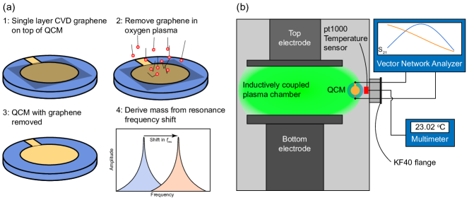
Figure 1(a) shows the experimental protocol to measure the mass of graphene. The crystal with CVD graphene is placed in the plasma chamber. Oxygen plasma etches the graphene and organic residues, which reduces the mass on top of the crystal that results in an increase of the QCM resonance frequency. The resonance frequency of the QCM is continuously monitored during the etching process. Stabilization of the resonance frequency indicates full removal of the graphene and all the organic contaminants from the QCM. The shift in the resonance frequency can be related to the removed mass using the Sauerbrey equation Sauerbrey (1959):
| (1) |
where is the density, the thickness of the material on top of the QCM, and the constant is given by the properties of the quartz crystal:
| (2) |
where is the density of quartz, the shear modulus and MHz the unloaded resonance frequency of the crystal. For the crystals used in this work, a single monolayer of graphene with a mass density of mg/m2 corresponds to a theoretical resonance frequency shift of 17.19 Hz.
Figure 1(b) shows the experimental setup to measure the resonance frequency of the crystal during etching. We use a reactive ion etcher (Leybold Hereaus Fluor F2) in a class 10000 (ISO7) cleanroom as the plasma chamber. A blind vacuum flange is adapted to create electrical feedthroughs to the chamber, and connected to a KF-40 port on the plasma chamber. A vector network analyzer (VNA) interrogates the resonance frequency of the membrane by a transmission measurement. Alternatively one can use a commercially available oscillator circuit as shown in the Supporting Information S1. However, the VNA produces the best results as it is not sensitive to the interference from the RF plasma at 13.56 MHz– the homodyne detection scheme rejects these frequencies. The oscillator circuit, on the other hand, will often lose lock on the mechanical resonance frequency when the plasma ignites, eliminating measurement data during the etching process (see Supporting Information S3). A pt-1000 temperature sensor is placed in the chamber near the crystal to monitor the temperature, because this affects the resonance frequency. The uncertainty in the resonance frequency is determined by three factors, as shown in the Supporting Information S2. First, the frequency dependence of the crystal on temperature, which is characetrized in a subsequent measurement. Second, the occurrence of a small (3 Hz) jump when the RF power is switched on, and third, the occurrence of random frequency jumps during the measurements which possibly occur due to spurious modes.
III Results
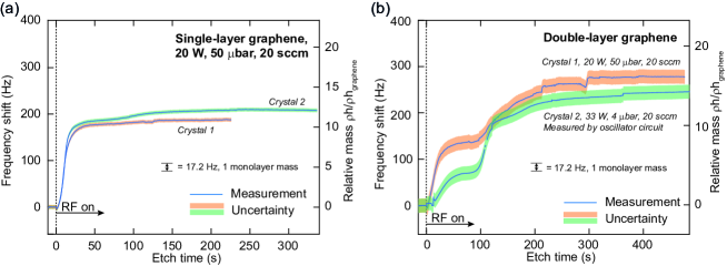
Figure 2 shows the resonance frequency of four graphene-covered sensors as a function of the etch time in an oxygen plasma. Samples covered with single-layer graphene are shown in Fig. 2(a) . After the plasma is switched on, the resonance frequency rapidly increases which indicates the removal of mass from the sensor. We observe that after approximately 20 seconds, the etch rate decreases considerably. After some time, however, the etch rate slightly increases again before the frequency stabilizes. In crystal 1, this corresponds roughly to a monolayer of graphene being etched, while in crystal 2 more mass is removed in this slower regime. A total mass corresponding to layers of graphene is removed from crystal 1, while a total of layers was removed from crystal 2. The total uncertainty of these measurements is determined to be 7 Hz, thus achieving sub-monolayer accuracy in the mass.
Results on the stacked double layers of graphene are shown in Fig. 2(b). Similar to the case of the single-layer graphene, the etching slows down considerably after approximately 40 to 50 seconds. After this, the etching rate increases significantly. In crystal 2, a second decrease in the etching rate is observed at approximately 130 seconds of etching time. Later, the etching rate increases again and finally stops. In crystal 1, this second decrease in etching rate is less prominent due to spurious frequency jumps near 200 seconds and 300 seconds. A total mass corresponding to monolayers of graphene is removed from crystal 1, while monolayers are removed from crystal 2. The more frequent occurrence of random jumps during the measurements of these samples cause a higher uncertainty compared to the single-layer crystals. Possible causes of the random jumps are outlined in the Supporting Information S2.
The total etched mass of all the sensors used in this work are shown in Table 1. The remaining etching curves that are not shown in Fig. 2 are given in the Supporting Information S3. For the double layer crystals, we etch away on average an equivalent mass of 16.7 monolayers of graphene while for the single layers we etch away 11.8 layers of graphene.
| Sample | SLG | DLG |
|---|---|---|
| 1 | 12.2† | 16.0† |
| 2 | 10.8† | 14.0‡ |
| 3 | 10.1‡ | 19.7‡ |
| 4 | 14.0‡ | 19.2‡ |
| 5 | 14.5‡ |
IV Discussion
We first discuss the observed variation in the etch rate, in particular the slow etching regimes in the double-layer samples. By comparing the single layer and double layer samples in Fig. 2, we conclude that the slower etch rate can be attributed to the graphene, since the double layer samples typically show a second decrease in the etching rate. The results thus show that graphene etching rate is much slower than the contamination. From the data with SLG in Fig. 2(a), we conclude that most of the contamination is present on the top side of the graphene since initially most of the mass is removed and after the etching slows down it does not increase again. This makes transfer residues from the polymer a likely source of the contamination. On Crystal 2 with SLG, significantly more mass (approximately 1.5 graphene monolayers) is removed in the slow etching regime, which might indicate the presence of contamination underneath the graphene. Possible sources of contamination underneath graphene could be water that is known to accumulate between graphene and the substrate Li et al. (2015), or insufficient cleaning of organic contaminants from the QCM before transfer. In the Supporting Information S3, we show a measurement at much lower plasma power of 4W. At these powers, graphene was not fully removed but rather oxidized as shown by Raman spectroscopy, confirming the slow etching rate of graphene with regard to the contamination.
The measurements of double layer graphene samples in Fig. 2(b) provide further evidence that the slower etch rate can be attributed to the graphene. One interpretation of the data is that the etching of the first graphene layer causes a significant decrease in the etching rate after 40 seconds and the less-prominent second decrease can be attributed to the second graphene layer. Since the etching rate significantly increases after slowing down, we conclude that the stacking of these layers effectively results (from bottom to top) in a graphene-residue-graphene-residue stack. While the first region with a slow etch rate shows a relatively sharp decrease in etching rate, the second slow regime is considerably smoother. This may be due to lateral non-uniformities in the etch rate or contamination thickness, which result in variations in the time when the second graphene layer is reached and etched. One striking observation is that the addition of the second graphene layer increases the mass by only 40%, instead of doubling the mass. From the experiments (Fig. 2) it appears that the additional mass can be attributed to the top contamination layer of the single layer graphene, while this layer is significantly thinner in the double-layer samples. The underlying cause of this observation is currently unknown.
The method presented here can be used in several future technological applications. For example, the frequency range of tunable oscillators Chen et al. (2013a); Davidovikj et al. (2018); Ye et al. (2017) and the responsivity of resonating pressure sensors Bunch et al. (2008); Dolleman et al. (2016, 2017b); Vollebregt et al. (2017) is significantly impacted by the mass-per-unit-square of the device. The method is also a useful technique to determine the presence of contamination. The electron mobility of graphene, for example, is significantly impacted by contaminants Pirkle et al. (2011); Suk et al. (2013); Chan et al. (2012); Goossens et al. (2012); Moser et al. (2007). Graphene has also been proposed as heat spreaders for thermal management in electronic circuits Ghosh et al. (2008), but contaminated samples also show a significantly lower thermal conductivity Pettes et al. (2011); Jo et al. (2015). For upscaling electronic and thermal graphene applications to the wafer scale, the proposed QCM method can be used to select the best transfer technique to produce high-quality graphene devices. Furthermore, the QCM method no longer requires the fabrication and testing of devices to optimize the transfer procedure Pirkle et al. (2011); Suk et al. (2013); Chan et al. (2012); Goossens et al. (2012); Moser et al. (2007), which simplifies the procedure and improves the throughput of the optimization process. The QCM method thus enables large-scale quality control of graphene sheets. Moreover, since graphene etches much slower than the contamination, the technique can discriminate between the amount of contamination underneath and on top of the graphene.
For research, the method is useful to study the mass of wrinkled graphene membranes to reveal their hidden area Nicholl et al. (2017), for example graphene transferred on smooth or rough substrates. Furthermore, the QCM measurement can be a corroboration to the number of layers revealed by Raman spectroscopy Ferrari et al. (2006). In particular, the method is accurate enough to count the number of layers on few-layer graphene samples, in the regime where this is difficult to achieve with Raman spectroscopy. Moreover in heterostructures or other stacks of multilayer 2D materials the QCMs are useful to reveal the presence of trapped residual materials, which can hamper the interlayer coupling that gives these stacks their favourable properties.
Future work on this QCM method can focus on high-temperature measurements, enabling one to study and optimize annealing proceduces to clean graphene Pirkle et al. (2011); Lin et al. (2011); Cartamil-Bueno et al. (2017). Recent advances in microbalance technology has resulted in GaPO4 crystals with operating temperatures exceeding 900∘C, which could even facilitate in-situ study of chemical vapour deposition of graphene on certain metal thin-films Thanner et al. (2002, 2003). Furthermore, the applicability of QCM’s in liquids could also be useful to study chemical cleaning of graphene Her et al. (2013); Liang et al. (2011); Suk et al. (2013) in-situ and optimize the process. This would in particular be interesting with regard to oxide and metal contaminants which are not removed by oxygen plasma. It would also be interesting to compare and benchmark transfer methods, for example transfer in air versus vacuum Lee et al. (2015) or wet versus dry transfer techniques.
V Conclusion
We present a method to determine the mass-per-unit-square and etch rate of CVD-grown graphene sheets using quartz crystal microbalances. This is achieved by etching graphene on a QCM in oxygen plasma and measuring the resonance frequency of the crystal in-situ. We find that by using a widely used dry transfer method, the mass of single-layer graphene sheet is observed to be ten times higher than the theoretical mass of graphene. The time-dependence of the etching rate shows that most of the contamination is on top of the graphene. The method is useful for quality control of large sheets of graphene for future sensing, electronic and thermal applications.
Acknowledgements
Acknowledgements.
The authors thank Applied Nanolayers B.V. for supply and transfer of the single-layer graphene and Hugo Solera Licona for help with cleaning the crystals. This work is part of the research programme Integrated Graphene Pressure Sensors (IGPS) with project number 13307 which is financed by the Netherlands Organisation for Scientific Research (NWO). The research leading to these results also received funding from the European Union’s Horizon 2020 research and innovation programme under grant agreement No 785219 Graphene Flagship. The authors acknowledge support from the Australian Research Council Centre of Excellence in Exciton Science (CE170100026) and the Australian Research Council Grants Scheme.Supporting Information
S1: Commercially available oscillator circuit
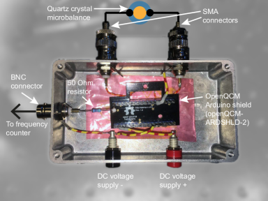
Part of the measurements in this work are performed by using a commercially available oscillator circuit mounted in a metal box as shown in Fig. 3. This is the openQCM Arduino shield (openQCM-ARDSHLD-2), where the crystal is normally mounted directly to the QCM using a holder. However, our application of the crystal in vacuum requires the PCB to be mounted outside the chamber. Therefore, the PCB is placed in a metal box and the connections, that normally connect directly to the crystal, are now connected to the center pins of two SMA connectors. SMA cables can then be connected to the KF-40 vacuum flange, which also uses SMA connections for the electrical feedthroughs. The DC voltage, that is normally supplied by an Arduino, is now supplied by an external voltage source (Rigol DP832A). A BNC connector carries the signal from the PCB to the frequency counter (Keysight 53230A) through a 50 Ohm resistor. This resistor matches to the load of the frequency counter and it is found that this drastically improves signal quality.
S2: Determination of uncertainty in the frequency shift
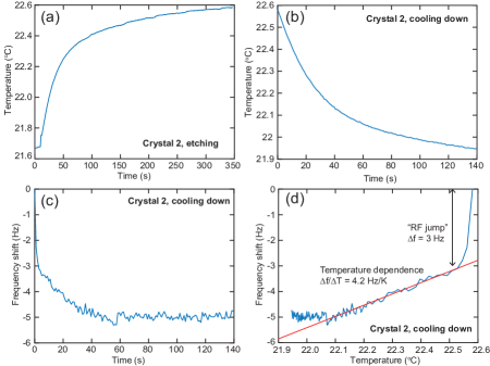
The quartz crystal microbalance is a highly sensitive platform for mass measurement, but is also sensitive to temperature and other effects which leads to some uncertainty in the measurements. For this reason, the temperature in the chamber is monitored during the etching as shown in Fig. 4(a). To give an estimate of the uncertainty, after each etching procedure the measurement of the frequency and temperature continued after the RF power was switched off. During this measurement the temperature drops (Fig. 4(b)) and a frequency shift is observed (Fig. 4(c)). Also, immediately after switching on the RF power a 3 Hz jump in the frequency is observed. The cause of this is not known, therefore we add this to the uncertainty as well. By plotting the frequency shift versus the temperature in Fig. 4(d), we determine the sensitivity of the resonance frequency to the temperature. In this crystal, the total temperature change during etching is 0.95K, resulting in a total temperature uncertainty of 4 Hz. The total uncertainty including the RF jump is then determined to be 7 Hz. In all crystals we found similar values.
For the double layer crystals the uncertainty is higher due to the occurrence of spontaneous jumps in the frequency. Most likely these can be attributed to spurious modes in the crystal or coupling to other modes. However, we cannot rule out that these jumps occur due to particles attaching or detaching to the crystal, therefore the height of these jumps was included in the uncertainty.
S3: Additional measurements
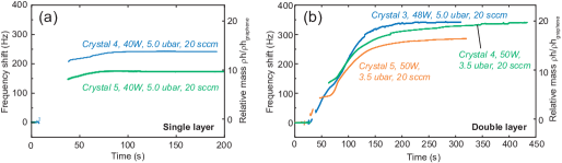
Figure 5 shows additional measurements that are included in Table 1 in the main section of the paper. These measurements are taken by the oscillator circuit, but we find that the oscillator circuit becomes often becomes unstable once the RF power is switched on, and the circuit has to be reset numerous times until it locks to the correct frequency. This leads to missing data points, however the start and end frequency still provide information of the amount of mass removed from the crystal. The problem is amended by using the vector network analyzer, alternatively one could use better holders to reject the interference from the electric field inside the plasma chamber.
Measurements at low power
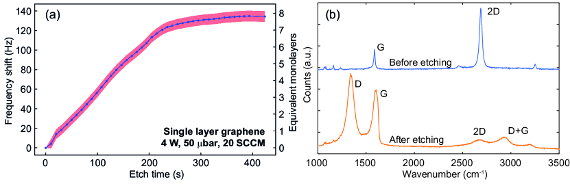
Figure 6(a) shows measurements at low RF powers of 4 W. We observe that the frequency increases and stabilizes at around 400 seconds. However, when Raman characterization was performed in Fig. 6(b), is it found that the graphene is not fully removed, and the Raman spectrum bears signatures of graphene oxide Wu et al. (2018). This shows that the graphene first oxidizes before it is removed from the system. In subbsequent measurements a higher power was used to ensure graphene is fully removed from the crystal.
Measurements on crystal without graphene
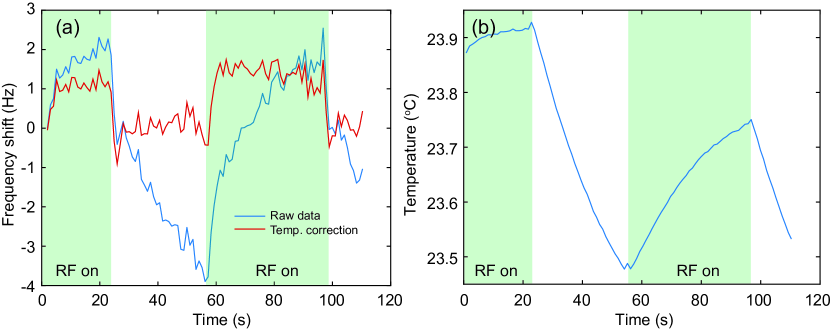
Figure 7 shows measurements on a crystal without graphene that has undergone the same cleaning procedure. The RF power was switched on and off to test whether the plasma could ignite in a stable manner with this recipe and to test the stability of the frequency measurement. The frequency changes considerably during the measurement, however this can be attributed to the temperature changes in the plasma chamber. Using the frequency as function of temperature when the plasma is off, the measurement can be corrected for the temperature (red line in Fig. 7(a)). In that case, the frequency shift is less than 0.2 Hz, which is neglectable compared to the other uncertainties in the system.
References
- Geim and Novoselov (2007) Andre K Geim and Konstantin S Novoselov, “The rise of graphene,” Nature Materials 6, 183–191 (2007).
- Neto et al. (2009) AH Castro Neto, F Guinea, NMR Peres, Kostya S Novoselov, and Andre K Geim, “The electronic properties of graphene,” Reviews of Modern Physics 81, 109 (2009).
- Balandin et al. (2008) Alexander A Balandin, Suchismita Ghosh, Wenzhong Bao, Irene Calizo, Desalegne Teweldebrhan, Feng Miao, and Chun Ning Lau, “Superior thermal conductivity of single-layer graphene,” Nano Letters 8, 902–907 (2008).
- Pop et al. (2012) Eric Pop, Vikas Varshney, and Ajit K Roy, “Thermal properties of graphene: Fundamentals and applications,” MRS Bulletin 37, 1273–1281 (2012).
- Dolleman et al. (2017a) Robin J Dolleman, Samer Houri, Dejan Davidovikj, Santiago J Cartamil-Bueno, Yaroslav M Blanter, Herre SJ van der Zant, and Peter G Steeneken, “Optomechanics for thermal characterization of suspended graphene,” Physical Review B 96, 165421 (2017a).
- Lee et al. (2008) Changgu Lee, Xiaoding Wei, Jeffrey W. Kysar, and James Hone, “Measurement of the elastic properties and intrinsic strength of monolayer graphene,” Science 321, 385–388 (2008).
- Davidovikj et al. (2017a) D. Davidovikj, F. Alijani, S. J. Cartamil-Bueno, H. S. J. van der Zant, M. Amabili, and P. G. Steeneken, “Nonlinear dynamic characterization of two-dimensional materials,” Nature Communications 8, 1253 (2017a).
- Sajadi et al. (2017) Banafsheh Sajadi, Farbod Alijani, Dejan Davidovikj, Johannes Goosen, Peter G Steeneken, and Fred van Keulen, “Experimental characterization of graphene by electrostatic resonance frequency tuning,” Journal of Applied Physics 122, 234302 (2017).
- Song et al. (2011) Xuefeng Song, Mika Oksanen, Mika A Sillanpaa, HG Craighead, JM Parpia, and Pertti J Hakonen, “Stamp transferred suspended graphene mechanical resonators for radio frequency electrical readout,” Nano Letters 12, 198–202 (2011).
- Chen et al. (2013a) Changyao Chen, Sunwoo Lee, Vikram V Deshpande, Gwan-Hyoung Lee, Michael Lekas, Kenneth Shepard, and James Hone, “Graphene mechanical oscillators with tunable frequency,” Nature Nanotechnology 8, 923–927 (2013a).
- Lemme et al. (2007) Max C Lemme, Tim J Echtermeyer, Matthias Baus, and Heinrich Kurz, “A graphene field-effect device,” IEEE Electron Device Letters 28, 282–284 (2007).
- Cartamil-Bueno et al. (2018) Santiago J. Cartamil-Bueno, Dejan Davidovikj, Alba Centeno, Amaia Zurutuza, Herre S. J. van der Zant, Peter G. Steeneken, and Samer Houri, “Graphene mechanical pixels for interferometric modulator displays,” Nature Communications 9, 4837 (2018).
- Dauber et al. (2015) Jan Dauber, Abhay A Sagade, Martin Oellers, Kenji Watanabe, Takashi Taniguchi, Daniel Neumaier, and Christoph Stampfer, “Ultra-sensitive Hall sensors based on graphene encapsulated in hexagonal boron nitride,” Applied Physics Letters 106, 193501 (2015).
- Smith et al. (2017) Anderson D Smith, Karim Elgammal, Xuge Fan, Max C Lemme, Anna Delin, Mikael Råsander, Lars Bergqvist, Stephan Schröder, Andreas C Fischer, Frank Niklaus, et al., “Graphene-based co 2 sensing and its cross-sensitivity with humidity,” RSC Advances 7, 22329–22339 (2017).
- Ricciardella et al. (2017) Filiberto Ricciardella, Sten Vollebregt, Tiziana Polichetti, Mario Miscuglio, Brigida Alfano, Maria L Miglietta, Ettore Massera, Girolamo Di Francia, and Pasqualina M Sarro, “Effects of graphene defects on gas sensing properties towards no 2 detection,” Nanoscale 9, 6085–6093 (2017).
- Smith et al. (2013) Anderson D Smith, Sam Vaziri, Frank Niklaus, Andreas C Fischer, Mikael Sterner, Anna Delin, Mikael Östling, and Max C Lemme, “Pressure sensors based on suspended graphene membranes,” Solid-State Electronics 88, 89–94 (2013).
- Dolleman et al. (2016) Robin J Dolleman, Dejan Davidovikj, Santiago J Cartamil-Bueno, Herre SJ van der Zant, and Peter G Steeneken, “Graphene squeeze-film pressure sensors,” Nano Letters 16, 568–571 (2016).
- Dolleman et al. (2017b) Robin J Dolleman, Santiago J Cartamil-Bueno, Herre S J van der Zant, and Peter G Steeneken, “Graphene gas osmometers,” 2D Materials 4, 011002 (2017b).
- Vollebregt et al. (2017) Sten Vollebregt, Robin J Dolleman, Herre S J van der Zant, Peter G Steeneken, and P M Sarro, “Suspended graphene beams with tunable gap for squeeze-film pressure sensing,” in Transducers 2017, The 19th International Conference on Solid-State Sensors, Actuators and Microsystems (IEEE, 2017) pp. 770–773.
- Davidovikj et al. (2017b) Dejan Davidovikj, Paul H Scheepers, Herre S J van der Zant, and Peter G Steeneken, “Static capacitive pressure sensing using a single graphene drum,” ACS Applied Materials & Interfaces 9, 43205–43210 (2017b).
- Suk et al. (2011) Ji Won Suk, Alexander Kitt, Carl W Magnuson, Yufeng Hao, Samir Ahmed, Jinho An, Anna K Swan, Bennett B Goldberg, and Rodney S Ruoff, “Transfer of CVD-grown monolayer graphene onto arbitrary substrates,” ACS Nano 5, 6916–6924 (2011).
- Li et al. (2009a) Xuesong Li, Weiwei Cai, Jinho An, Seyoung Kim, Junghyo Nah, Dongxing Yang, Richard Piner, Aruna Velamakanni, Inhwa Jung, Emanuel Tutuc, et al., “Large-area synthesis of high-quality and uniform graphene films on copper foils,” Science 324, 1312–1314 (2009a).
- Li et al. (2009b) Xuesong Li, Yanwu Zhu, Weiwei Cai, Mark Borysiak, Boyang Han, David Chen, Richard D Piner, Luigi Colombo, and Rodney S Ruoff, “Transfer of large-area graphene films for high-performance transparent conductive electrodes,” Nano letters 9, 4359–4363 (2009b).
- Lee et al. (2010) Youngbin Lee, Sukang Bae, Houk Jang, Sukjae Jang, Shou-En Zhu, Sung Hyun Sim, Young Il Song, Byung Hee Hong, and Jong-Hyun Ahn, “Wafer-scale synthesis and transfer of graphene films,” Nano Lletters 10, 490–493 (2010).
- Chen et al. (2013b) Xu-Dong Chen, Zhi-Bo Liu, Chao-Yi Zheng, Fei Xing, Xiao-Qing Yan, Yongsheng Chen, and Jian-Guo Tian, “High-quality and efficient transfer of large-area graphene films onto different substrates,” Carbon 56, 271–278 (2013b).
- Zande et al. (2010) Arend M van der Zande, Robert A Barton, Jonathan S Alden, Carlos S Ruiz-Vargas, William S Whitney, Phi HQ Pham, Jiwoong Park, Jeevak M Parpia, Harold G Craighead, and Paul L McEuen, “Large-scale arrays of single-layer graphene resonators,” Nano Letters 10, 4869–4873 (2010).
- Her et al. (2013) Michael Her, Ryan Beams, and Lukas Novotny, “Graphene transfer with reduced residue,” Physics Letters A 377, 1455–1458 (2013).
- Lin et al. (2011) Yung-Chang Lin, Chun-Chieh Lu, Chao-Huei Yeh, Chuanhong Jin, Kazu Suenaga, and Po-Wen Chiu, “Graphene annealing: how clean can it be?” Nano letters 12, 414–419 (2011).
- Pirkle et al. (2011) A Pirkle, J Chan, A Venugopal, D Hinojos, CW Magnuson, S McDonnell, L Colombo, EM Vogel, RS Ruoff, and RM Wallace, “The effect of chemical residues on the physical and electrical properties of chemical vapor deposited graphene transferred to sio2,” Applied Physics Letters 99, 122108 (2011).
- Suk et al. (2013) Ji Won Suk, Wi Hyoung Lee, Jongho Lee, Harry Chou, Richard D Piner, Yufeng Hao, Deji Akinwande, and Rodney S Ruoff, “Enhancement of the electrical properties of graphene grown by chemical vapor deposition via controlling the effects of polymer residue,” Nano letters 13, 1462–1467 (2013).
- Chan et al. (2012) Jack Chan, Archana Venugopal, Adam Pirkle, Stephen McDonnell, David Hinojos, Carl W Magnuson, Rodney S Ruoff, Luigi Colombo, Robert M Wallace, and Eric M Vogel, “Reducing extrinsic performance-limiting factors in graphene grown by chemical vapor deposition,” ACS nano 6, 3224–3229 (2012).
- Goossens et al. (2012) AM Goossens, VE Calado, A Barreiro, K Watanabe, T Taniguchi, and LMK Vandersypen, “Mechanical cleaning of graphene,” Applied Physics Letters 100, 073110 (2012).
- Moser et al. (2007) Joel Moser, Amelia Barreiro, and Adrian Bachtold, “Current-induced cleaning of graphene,” Applied Physics Letters 91, 163513 (2007).
- Pettes et al. (2011) Michael Thompson Pettes, Insun Jo, Zhen Yao, and Li Shi, “Influence of polymeric residue on the thermal conductivity of suspended bilayer graphene,” Nano Letters 11, 1195–1200 (2011).
- Jo et al. (2015) Insun Jo, Michael T Pettes, Lucas Lindsay, Eric Ou, Annie Weathers, Arden L Moore, Zhen Yao, and Li Shi, “Reexamination of basal plane thermal conductivity of suspended graphene samples measured by electro-thermal micro-bridge methods,” AIP Advances 5, 053206 (2015).
- Bunch et al. (2008) J Scott Bunch, Scott S Verbridge, Jonathan S Alden, Arend M Van Der Zande, Jeevak M Parpia, Harold G Craighead, and Paul L McEuen, “Impermeable atomic membranes from graphene sheets,” Nano Letters 8, 2458–2462 (2008).
- Singh et al. (2010) Vibhor Singh, Shamashis Sengupta, Hari S Solanki, Rohan Dhall, Adrien Allain, Sajal Dhara, Prita Pant, and Mandar M Deshmukh, “Probing thermal expansion of graphene and modal dispersion at low-temperature using graphene nanoelectromechanical systems resonators,” Nanotechnology 21, 165204 (2010).
- Barton et al. (2012) Robert A Barton, Isaac R Storch, Vivekananda P Adiga, Reyu Sakakibara, Benjamin R Cipriany, B Ilic, Si Ping Wang, Peijie Ong, Paul L McEuen, Jeevak M Parpia, and Harold G. Craighead, “Photothermal self-oscillation and laser cooling of graphene optomechanical systems,” Nano Letters 12, 4681–4686 (2012).
- Chen et al. (2009) Changyao Chen, Sami Rosenblatt, Kirill I Bolotin, William Kalb, Philip Kim, Ioannis Kymissis, Horst L Stormer, Tony F Heinz, and James Hone, “Performance of monolayer graphene nanomechanical resonators with electrical readout,” Nature Nanotechnology 4, 861–867 (2009).
- Ferrari et al. (2006) AC Ferrari, JC Meyer, V Scardaci, C Casiraghi, Michele Lazzeri, Francesco Mauri, S Piscanec, Da Jiang, KS Novoselov, S Roth, and AK Geim, “Raman spectrum of graphene and graphene layers,” Physical Review Letters 97, 187401 (2006).
- Blake et al. (2007) P Blake, E W Hill, AH Castro Neto, K S Novoselov, D Jiang, R Yang, T J Booth, and AK Geim, “Making graphene visible,” Applied Physics Letters 91, 063124 (2007).
- Nemes-Incze et al. (2008) P Nemes-Incze, Z Osváth, K Kamarás, and LP Biró, “Anomalies in thickness measurements of graphene and few layer graphite crystals by tapping mode atomic force microscopy,” Carbon 46, 1435–1442 (2008).
- Nicholl et al. (2015) Ryan JT Nicholl, Hiram J Conley, Nickolay V Lavrik, Ivan Vlassiouk, Yevgeniy S Puzyrev, Vijayashree Parsi Sreenivas, Sokrates T Pantelides, and Kirill I Bolotin, “The effect of intrinsic crumpling on the mechanics of free-standing graphene,” Nature communications 6, 8789 (2015).
- Lee et al. (2012) Jae-Ung Lee, Duhee Yoon, and Hyeonsik Cheong, “Estimation of Young’s modulus of graphene by Raman spectroscopy,” Nano Letters 12, 4444–4448 (2012).
- Ruiz-Vargas et al. (2011) Carlos S Ruiz-Vargas, Houlong L Zhuang, Pinshane Y Huang, Arend M Van Der Zande, Shivank Garg, Paul L McEuen, David A Muller, Richard G Hennig, and Jiwoong Park, “Softened elastic response and unzipping in chemical vapor deposition graphene membranes,” Nano letters 11, 2259–2263 (2011).
- Davidovikj et al. (2016) Dejan Davidovikj, Jesse J Slim, Santiago J Cartamil-Bueno, Herre S J van der Zant, Peter G Steeneken, and Warner J Venstra, “Visualizing the motion of graphene nanodrums,” Nano Letters 16, 2768–2773 (2016).
- Wong et al. (2010) CL Wong, M Annamalai, ZQ Wang, and M Palaniapan, “Characterization of nanomechanical graphene drum structures,” Journal of Micromechanics and Microengineering 20, 115029 (2010).
- Sauerbrey (1959) Günter Sauerbrey, “Verwendung von schwingquarzen zur wägung dünner schichten und zur mikrowägung,” Zeitschrift für Physik 155, 206–222 (1959).
- O’sullivan and Guilbault (1999) CK O’sullivan and GG Guilbault, “Commercial quartz crystal microbalances–theory and applications,” Biosensors and bioelectronics 14, 663–670 (1999).
- Buttry and Ward (1992) Daniel A Buttry and Michael D Ward, “Measurement of interfacial processes at electrode surfaces with the electrochemical quartz crystal microbalance,” Chemical Reviews 92, 1355–1379 (1992).
- Li et al. (2015) Qiang Li, Jie Song, Flemming Besenbacher, and Mingdong Dong, “Two-dimensional material confined water,” Accounts of Chemical Research 48, 119–127 (2015).
- Davidovikj et al. (2018) Dejan Davidovikj, Menno Poot, Santiago J Cartamil-Bueno, Herre SJ van der Zant, and Peter G Steeneken, “On-chip heaters for tension tuning of graphene nanodrums,” Nano Letters 18, 2852–2858 (2018).
- Ye et al. (2017) Fan Ye, Jaesung Lee, and Philip X-L Feng, “Very-wide electrothermal tuning of graphene nanoelectromechanical resonators,” in Micro Electro Mechanical Systems (MEMS), 2017 IEEE 30th International Conference on (IEEE, 2017) pp. 68–71.
- Ghosh et al. (2008) S Ghosh, I Calizo, D Teweldebrhan, EP Pokatilov, DL Nika, AA Balandin, W Bao, F Miao, and C Ning Lau, “Extremely high thermal conductivity of graphene: Prospects for thermal management applications in nanoelectronic circuits,” Applied Physics Letters 92, 151911 (2008).
- Nicholl et al. (2017) Ryan J. T. Nicholl, Nickolay V. Lavrik, Ivan Vlassiouk, Bernadeta R. Srijanto, and Kirill I. Bolotin, “Hidden area and mechanical nonlinearities in freestanding graphene,” Physical Review Letters 118, 266101 (2017).
- Cartamil-Bueno et al. (2017) Santiago J Cartamil-Bueno, Matteo Cavalieri, Ruizhi Wang, Samer Houri, Stephan Hofmann, and Herre SJ van der Zant, “Mechanical characterization and cleaning of cvd single-layer h-bn resonators,” npj 2D Materials and Applications 1, 16 (2017).
- Thanner et al. (2002) H Thanner, PW Krempl, W Wallnöfer, and PM Worsch, “Gapo4 high temperature crystal microbalance with zero temperature coefficient,” Vacuum 67, 687–691 (2002).
- Thanner et al. (2003) H. Thanner, P. W. Krempl, R. Selic, W. Wallnöfer, and P. M. Worsch, “GaPO4 high temperature crystal microbalance demonstration up to 720∘C,” Journal of Thermal Analysis and Calorimetry 71, 53–59 (2003).
- Liang et al. (2011) Xuelei Liang, Brent A Sperling, Irene Calizo, Guangjun Cheng, Christina Ann Hacker, Qin Zhang, Yaw Obeng, Kai Yan, Hailin Peng, Qiliang Li, et al., “Toward clean and crackless transfer of graphene,” ACS nano 5, 9144–9153 (2011).
- Lee et al. (2015) Sangchul Lee, Sang Kyung Lee, Chang Goo Kang, Chunhum Cho, Young Gon Lee, Ukjin Jung, and Byoung Hun Lee, “Graphene transfer in vacuum yielding a high quality graphene,” Carbon 93, 286 – 294 (2015).
- Wu et al. (2018) Jiang-Bin Wu, Miao-Ling Lin, Xin Cong, He-Nan Liu, and Ping-Heng Tan, “Raman spectroscopy of graphene-based materials and its applications in related devices,” Chem. Soc. Rev. 47, 1822–1873 (2018).