Low temperature ( 200∘C) solution processed tunable flash memory device without tunneling and blocking layer
Intrinsic charge trap capacitive non-volatile flash memories take a significant share of the semiconductor electronics market today. It is a challenge to create intrinsic traps in the dielectric layer without high temperature processing stepsHsinChiangYou2006 . While low temperature processed memory devices fabricated from polymers have been demonstrated as an alternativeLee2007 ; Kapetanakis2008 ; Tsai2013 ; Chiu2014a ; Chiu2015 ; Wei2012 , their performance degrade rapidly after a few cycles of operationBaeg2014 ; Park2015a ; Kim2010a ; Faber2009 ; Park2010c ; Han2011a ; Wang2010 . Moreover conventional memory devices need the support of tunneling and blocking layers since the memory dielectric or polymer is incapable of preventing memory leakageKim2010b ; Yi2016a ; Lee2009 . The main issue in designing a memory device is to optimize the leakage current and intrinsic trap density simultaneouslyLee2011b . Here we report a tunable flash memory device without tunneling and blocking layer by combining the discovery of high intrinsic charge traps (1012 cm-2) together with low leakage current(10-7 A.cm-2) in solution derived, inorganic, spincoated dielectric films which were heated at 200∘C or below. In addition, the memory storage is tuned systematically upto 96% by controlling the trap density with increasing heating temperature.
Today’s semiconductor memory technology is dominated by silicon-oxide-nitride-oxide-silicon (SONOS) non-volatile flash memory which is based on intrinsic charge traps in silicon-rich silicon nitride films deposited by high temperature ( 780oC) compatible chemical vapor depositionXue2012 ; Liu2012 . The intrinsic charge traps in silicon-rich silicon nitride films were first reported in 1967 Hu1967 and the first flash memory device incorporating silicon nitride charge storage was demonstrated in 1980’s Junction1989 . However the trap density and distribution are difficult to control in such materialPark2006 . Traps can be increased by ion bombardment and plasma-passivationLiu2012 , but the leakage current increases. Alternate high-k dielectrics such as TiO2, HfO2, ZrO2, etc. are excellent insulators for transistor applications Avis2011 ; Suzuki2009b ; Dutta2013a ; Kumar2015a , but do not have the intrinsic charge trapping properties as silicon nitride. Although solution processed HfO2 has been used to fabricate SONOS type flash memoryHsinChiangYou2006 , the devices required the support of additional dielectric layers which were deposited by sophisticated ultrahigh vacuum techniques with high temperature processing steps to improve the memory leakage. For most dielectrics, precursor solutions with organic solvents result in poor leakage current which can be improved to some extent by high heating temperatureMondal2017 . However the high temperature heating process lowers leakage current but reduces trap density. Hence, the main challenge is to simultaneously achieve deep intrinsic charge traps together with very low leakage current at low processing temperatures. There are a few reports on solution processed flash memory by using polymer materialsChang2013 ; Shih2015 , but these devices degrade after only few cycles of operation in normal environmental conditions and they are not capable of working at higher temperatures.
In the last few years, a novel inorganic, completely carbon free, water soluble dielectric Aluminium Oxide Phosphate (ALPO), has been successfully employed as gate dielectric in high performance TFTs that are competitive with a-Si TFTsKim2011 . Due to its very low leakage current density, it was used recently as tunneling and blocking layer to fabricate fully solution processed two terminal capacitive flash memory devicesMondal2016 with CdTe-NP as the charge storage center. Nevertheless a fully spincoated low temperature processed (below 200∘C) highperformance flash memory device without tunneling and blocking layers has not been reported so far.
Here we report the discovery of ultra-high number of intrinsic charge traps (1012cm-2) in low temperature solution processed inorganic ALPO dielectric. At the same time, the leakage current is sufficiently low ( 10-7 A.cm-2) for flash memory operation without incorporating tunneling or blocking layers. In addition, the number of traps can be varied with heating temperature, which is strongly correlated with the oxygen vacancy concentration in the film. Furthermore, we demonstrate optimized robust high performance fully solution processed inorganic oxide precursor based flash memory devices without tunneling and blocking layer, where the processing temperature does not exceed 200∘C. Our devices outperform other similar memory devices reported earlierLee2007 ; Kapetanakis2008 ; Tsai2013 ; Chiu2014a ; Chiu2015 ; Wei2012 .
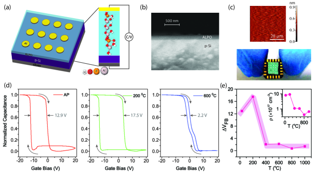
A schematic of typical device architecture is depicted in Fig. 1a. ALPO is deposited by spin-coating a completely inorganic, carbon free and aqueous precursor solution on low-doped -silicon substrate (41015 cm-3). After deposition various substrates are heated at different temperatures including at low temperature such as 200∘C. The inset of Fig. 1a shows a schematic of molecular structure of the low temperature (200∘C) processed ALPO. The thickness of the deposited film is measured by ellipsometry (see Section I, Supporting Information) and verified by cross-sectional scanning electron microscope (SEM) image (Fig. 1b). Such prepared films are found to be atomically smooth showing surface roughness to be 0.08 nmMeyers2007a ; Mondal2017 which is determined by the atomic force microscopy (AFM) with an areal scan over 50m50m (top-panel,Fig. 1c). An aluminum contact is deposited thereafter by thermal evaporation for the purpose of electrical measurement. The deep level charge storage in the deposited ALPO is characterized via capacitance-voltage (CV) measurement. An optical image of device on chip has been shown in the bottom-panel of Fig. 1c.
Intrinsic trap levels in ALPO cause a hysteretic output of the CV traces highlighting the memory-like behavior of the devices (Fig. 1d). Further, the trap density can be varied by heating the samples at different temperatures which alters the hysteresis-window. For example, an as-prepared sample shows a memory window of 12.9 V (left-panel) which corresponds to a trap density of n 5.651012 cm-2, where as, an ALPO-film heated at 200∘C for one hour shows a hysteresis window of 17.5 V which corresponds to the trap density of n 6.371012 cm-2. When the film is heate at 600∘C, the trap density drastically reduces (n cm-2) causing a significantly low hysteresis window ( V, right-panel). A similar variation of electronic traps with heating temperature is also observed from the devices which are made with lower thickness ALPO film, however, there is no affect due to change in device dimension (see Section III, Supporting Information). From the sweep direction of the CV curve it is inferred that gate injection of carriers controls the memory operation. Although conventional flash memory architecture follows channel injection of carriersLiu2012 , the interface degrades fast in such devicesWu2008 . Thus, compared to channel injected devices, gate-injected devices show higher endurance which is one of the key requirements of memory operationLue2007 . Because of such advantages, the quest for efficient gate-injected flash memory devices is ongoingWu2008 ; Lue2007 ; Lue2008 ; YeolYun2014 . A systematic change in the hysteresis window as a function of heating temperature is presented in Fig. 1e, where, solid squares are the experimental data, shaded region is guide to the eye and the width of the shaded region indicate the standard deviation around their mean vertical position estimated from similar results. Use of higher heating temperature (C) causes a dramatic reduction in trap density, thus reducing the hysteresis window. A 96% reduction in trap density (1011 cm-2) is observed at an heating temperature of 800∘C resulting a memory window of 0.7 V only. In addition, a negligible degradation in CV hysteresis is obtained from as prepared devices even after 5 years of storage in ambient conditions (see Section IV, Supporting Information). This demonstrates that the devices are very stable for long term application, in spite of the water absorbing property of ALPOPerkins2016 ; Anderson2015 .
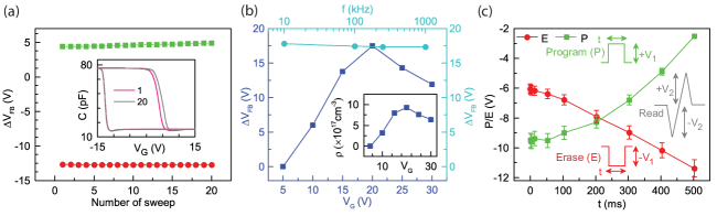
In order to investigate the robustness of intrinsic charge storage property of ALPO, we demonstrate a series of memory operations on the metal-insulator-semiconductor structured (MIS) two terminal capacitive devices which were heated at 200∘C. The memory characterization focuses upon the flat band voltage shift (VFB) due to the voltage sweep operation (i.e. erasing() or programming() operation) on the gate terminal of the devices. A device is programmed () or erased () by sweeping the gate voltage at a slow rate Mondal2016 . Sequential and cycles set and reset the flat band voltage reversibly and is confirmed from the nearly constant values obtained from multiple - cycles (Fig. 2a). Two of the - traces corresponding to the 1st and 20th - traces are shown in the inset of Fig. 2a. Nearly constant values of in and states indicate that - cycles have negligible effect on the memory state thus indicating high reliability of the devices.
Frequency and gate bias dependent changes are shown in Fig. 2b. Flatband voltage window shows insignificant change within the range of 10-1000 kHz frequency of excitation voltage. Such behavior is attributed to the slow trapping de-trapping phenomena which thus indicates that the states can be probed by deploying high speed CV measurement. With different gate bias voltages increases first and then shows a decrease. Such behavior appears because of the competition between the trap filling and charge losses. Initially (5-20 V) as the sweep voltage is increased, larger electric field causes more charge injection into the traps, hence, the hysteresis width increases. Beyond 20 V, which corresponds to an electric field of 1.2 MV.cm-1), the high leakage current (see Section V, Supporting Information) leads to increased charge loss, thus a reduction in hysteresis window is observed (Fig. 2b). A hysteresis window of 15 V is obtained for a sweep voltage range of 15 V which corresponds to an optimum memory window of 50% of the total sweep-range. The result of 50% window for intrinsic traps in ALPO exceeds previously reported valuesLehninger2015c for other dielectrics. It is known from literature that the high performance operation of flash memory stack should not have leakage current density more than 10-6 A.cm-2 when operated with an electric field of 1 MV.cm-1 ChiChangWu2010 . The ALPO devices show a leakage current density of 4.510-8 A.cm-2 only at -1 MV.cm-1 electric field. Such low leakage current not only meets the criteria for the application of high-performance flash memory devices, but also outperforms other solution processed inorganic dielectrics namely Al2O3Avis2011 , HfO2Suzuki2009b , ZrO2Dutta2013a , and TiO2Kumar2015a , which show typical leakage currents 10-5 A.cm-2, 10-7 A.cm-2, 10-2 A.cm-2 and 10-5 A.cm-2 respectively at 1 MV cm-1. This observation for ALPO also ensures that high quality flash memory devices can be fabricated without the need of blocking or tunneling layers.
True program () and erase () operations are realized by application of positive and negative square pulses respectively, Whereas the read operation is performed by using triangular pulses having shorter time periods (T 4 s). Since high speed voltage sweep does not alter the memory state (Fig. 2b), shorter triangular pulses are expected to probe the and states without disturbing them. By varying the width of the square-pulses, various memory-windows () are obtained and shown in Fig. 2c. While using a single pulse to program or erase, a pulse width of 500 ms can set the memory window to be as large as 9 V. The program/erase speed of these devices is found to be 200 ms which is significantly faster compared to other solution processed flash memory devicesLehninger2015c ; Park2014 ; Yun2009 ; Bar2015c ; Chen2011 . During programming and erasing, a maximum charge capturing efficiency of 7.46 % is estimated while operating with a gate electric field of 2.37 MV/cm (see Section VI, Supporting Information). This capturing efficiency is higher than the reported values obtained from other dielectricsZhang2007 .
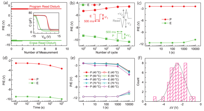
To check for any disturbance of the program/erase state during the read operation, the device is set to or states first with a single long square pulse (s, see Fig. 2c) and then multiple high-frequency triangular (s) pulses were applied representing multiple read operations. Figure 3a shows the statistical distribution of values obtained from such multiple read operations for both the and states. Narrow distributions of indicate low read-disturb for both the states. Inset of Fig. 3a shows typical - traces for , and read operations. Here two red and two green lines indicate back-and-forth sweep of the voltage () using the high speed triangular read pulse probing the and states respectively.
Erase-program operation over 10 k cycles shows no degradation in memory window thus demonstrates high endurance (Fig. 3b). In fact, with the increasing operation cycle memory window increases which may be attributed to the generation of additional trap states because of electrical stress. Data retention was tested by programming a fresh device at room temperature with pulses of amplitude 33 V and duration 500 ms. The device shows almost no change in memory window within 104s which was the limit of experimental time scale. This is the highest reported retention time for any memory device without additional tunneling and blocking layers. Even after 10 k / cycles devices show a degradation of only 9% memory window after s (Fig. 3d). Temperature dependent data retention was also tested and presented in Fig. 2e. After 104s of operation a memory window loss of 25% and 50% are observed at 60∘C and 80∘C respectively. The reliability is also tested on the device made with lower thickness of ALPO film (91 nm) which shows equivalent performance as obtained from the other devices(see Section VII, Supporting Information)
To examine the scalability of these low temperatures processed memory devices, we prepared and characterized more than 40 devices. Statistical distribution of memory window for all these devices are shown in Fig. 3f. 80% of devices lie within the expected memory window (3-4V) when programmed with 33 V pulse height and 300 ms duration. The remaining 20% devices show a memory window of less than 3V. These preliminary results show sufficiently high yield for large scale production needed for practical applications.
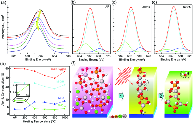
Microscopic origin of memory operation is understood from the temperature controlled trap density variation which is confirmed from photo-emission spectroscopy (XPS). Multiple samples were prepared at different heating temperatures and studied with XPS. The shape of the oxygen peak changes systematically with respect to heating temperature (Fig. 4a). De-convolution of XPS signal into respective peaks of oxygen vacancies(M-Ovac), metal hydroxide(M-OH) and lattice oxygen(M-O) helps understanding the contributions of respective states (Fig. 4b-d). The ALPO film which was heated at 200∘C has similar ratio (atomic %) of aluminum (Al), oxygen (O) and phosphorous (P) as that of the mother solution (see Section VIII, Supporting Information). Due to addition of HCl in the ALPO precursor, a small percentage of chlorine is observed (see Section IX, Supporting Information) in low temperature processed ALPO film. It is observed that M-Ovac intensity sharply decreases with increase in heating where temperature reaches above 200∘C (Fig. 4b-d and Section X of Supporting Information). As the heating temperature increases, hydrogen is lost as water vapor and the film becomes denser. The M-O peaks increase with higher heating temperature (Fig. 4e-f ). This is consistent with the reduction in the number of oxygen vacancies and consequently lower trap density in samples heated at higher temperature. A quantitative comparison between the peak intensity and the trap density of the heated film reveals a strong correlation between the oxygen vacancies and trap densities (see Section X, Supporting Information), thus indicating that the oxygen vacancies are the responsible entities for memory states.
In conclusion we have shown fabrication and high quality performance of low temperature processed (200 ∘C) inorganic flash memory devices which do not require tunneling or blocking layers. Simple sample fabrication technique involving spin-coating of solution is another advantage. Narrow distribution of memory window obtained from more than 40 samples indicates the scalability of the fabrication method. In spite of having no tunneling and blocking layers, these devices show extremely low leakage current which is one of the key features of memory operation, and demonstrate high endurance, high retention, thus, outperforming other solution processed memory devices reported so far. Temperature dependent control on trap density also helps optimizing the memory window. ALPO based devices paves the way for designing a new class of scalable two terminal flash memory devices for practical applications.
Table - I Memory Technology Comparison Device Fab. Technique Structure P/E Vol (V) P/E Time Memory Window Ref. ALD & RF Sputtering p-Si/SiO2/Ge-NC/TaZrOx/Al2O3/Al 10 V 60 s 3.8 V Lehninger2015c PECVD & Thermal Si/SiO2/Al@Al2O3-NP/SiO2/Al 15 V 5 s / 5 s 2.5 V Park2014 PVD & e-beam p-Si/Al2O3/Pt-NP/Al2O3/Ti 7 V 5 s / 5 s 4.3 V Yun2009 RF Sputtering p-Si/Al2O3/GeNC1L/Al2O3/Al 5 V / -5 V 3 s / 3 s 2.3 V Bar2015c PECVD & Sputtering p-Si/SiO2/DyTixOy/Al2O3/Al 7 V / -10 V 1 s / 10 s 4V Chen2011 Solution Processed p-Si/ALPO/Al 30 V / -30V 500 ms / 500 ms 9 V This work
Methods
Material growth: Precursor solution of Aluminium Oxide Phosphate, ALPO [Al2O3-3X (PO4)2X] in water (18 M cm) was prepared with Al(OH)3 (99%, Alfa Aesar, USA) in 2 mole equivalents of HCl (AR Grade, Thermo Fisher Scientific, USA) and an appropriate amount of H3PO4 (ExcelaR Grade, Thermo Fisher Scientific, USA) was added to obtain P/Al = 0.5 with concentration of 0.5 M . The solution was stirred under heat of 90∘C in a water bath for 24 hours.
Device fabrication: Two terminal MIS structures were fabricated on piranha cleaned [H2SO4:H2O2 = 3:1] lightly doped silicon substrate (pSi). The ALPO solution was spin-coated at 3000 rpm for 30s to form the gate dielectric. The films were then heated at 150oC for 1 min. This process was repeated for 2-3 times to achieve the desired thickness. The sample was exposed to oxygen plasma for 5 to 10 mins at 0.5 mbar pressure before deposition of each layer. Such fabrication process may help generation of stable traps in ALPO below 200∘C. Typically, ALPO based devices are treated at high temperature (350∘C) to achieve better dielectric performance, thus, most of the reported devices do not show any memory effectKim2011 . For control devices the film was further heated at 800oC for one hour in ambient to achieve the trap free oxide. A 200 nm aluminium gate was deposited by thermal evaporation at 10-6 mbar pressure. Before deposition of the top aluminium gate, the ALPO films were heated at different temperature in a preheated furnace for one hour. All devices were stored under ambient conditions and no degradation of CV curves was found even after three years.
Characterization: ALPO precursor solutions prepared with different concentrations and P/Al ratios were optically characterized using a UV-Visible spectrophotometer. They are all transparent in visible wavelength range with the main absorption peak in the ultra-violet range at 235 nm. After spin coating and heating, the film shows a refractive index 1.5 (see Section I, Supporting Information) with negligible absorption at 550 nm as measured by ellipsometry (M-2000, J.A. Woollam Co. Inc., USA). The thickness of ALPO film on silicon substrate extracted from ellipsometry is 139 nm and verified with cross-sectional SEM (Ultra 55, Carl Zeiss). The surface of the ALPO film is atomically smooth with a roughness of 0.08 nm as measured by AFM (NDMDT, Russia). The CV curve was measured with HIOKI 3532 LCR meter and Keithley 2400 source meter. Agilent Device Analyzer B1500A was used to measure the IV characteristics in ambient environment. The leakage current and CV measurements were performed on more than 50 devices. The entire measurement was done in continuous mode of the instrument. The high speed CV measurement was performed with home made CV measurement systemMondal2016 . The XPS measurements were carried out by AXIS 165 with Al K radiation (9mA, 13keV, 1486.6 eV) in ultrahigh vacuum. The XPS spectra were calibrated with C 1s peak (284.6 eV).
References
- (1) Hsin-Chiang You et al. SONOS-type flash memory using an HfO$_2$ as a charge trapping layer deposited by the sol-gel spin-coating method. IEEE Electron Device Letters 27, 653–655 (2006).
- (2) Lee, J.-S. et al. Layer-by-layer assembled charge-trap memory devices with adjustable electronic properties. Nature Nanotechnology 2, 790–795 (2007).
- (3) Kapetanakis, E. et al. Molecular storage elements for proton memory devices. Advanced Materials 20, 4568–4574 (2008).
- (4) Tsai, T.-D., Chang, J.-W., Wen, T.-C. & Guo, T.-F. Manipulating the Hysteresis in Poly(vinyl alcohol)-Dielectric Organic Field-Effect Transistors Toward Memory Elements. Advanced Functional Materials 23, 4206–4214 (2013).
- (5) Chiu, Y. C., Otsuka, I., Halila, S., Borsali, R. & Chen, W. C. High-performance nonvolatile transistor memories of pentacence using the green electrets of sugar-based block copolymers and their supramolecules. Advanced Functional Materials 24, 4240–4249 (2014).
- (6) Chiu, Y. C. et al. Oligosaccharide Carbohydrate Dielectrics toward High-Performance Non-volatile Transistor Memory Devices. Advanced Materials 27, 6257–6264 (2015).
- (7) Wei, Q. et al. Additive-driven assembly of block copolymer-nanoparticle hybrid materials for solution processable floating gate memory. ACS Nano 6, 1188–1194 (2012).
- (8) Baeg, K. J. et al. Charge-Trap Flash-Memory Oxide Transistors Enabled by Copper-Zirconia Composites. Advanced Materials 26, 7170–7177 (2014).
- (9) Park, Y.-S. & Lee, J.-S. Design of an Efficient Charge-Trapping Layer with a Built-In Tunnel Barrier for Reliable Organic-Transistor Memory. Advanced Materials 27, 706–711 (2015).
- (10) Kim, S. J. & Lee, J. S. Flexible organic transistor memory devices. Nano Letters 10, 2884–2890 (2010).
- (11) Faber, H. et al. Low-Temperature Solution-Processed Memory Transistors Based on Zinc Oxide Nanoparticles. Advanced Materials 21, 3099–3104 (2009).
- (12) Park, Y. S. et al. High-performance organic charge trap flash memory devices based on ink-jet printed 6,13-bis(triisopropylsilylethynyl) pentacene transistors. Applied Physics Letters 96, 1–4 (2010).
- (13) Han, S.-T., Zhou, Y., Xu, Z.-X., Roy, V. A. L. & Hung, T. F. Nanoparticle size dependent threshold voltage shifts in organic memory transistors. Journal of Materials Chemistry 21, 14575 (2011).
- (14) Wang, S. M., Leung, C. W. & Chan, P. K. Nonvolatile organic transistor-memory devices using various thicknesses of silver nanoparticle layers. Applied Physics Letters 97 (2010).
- (15) Kim, Y. M., Kim, S. J. & Lee, J. S. Organic-transistor-based nano-floating-gate memory devices having multistack charge-trapping layers. IEEE Electron Device Letters 31, 503–505 (2010).
- (16) Yi, M. et al. The effect of porous structure of PMMA tunneling dielectric layer on the performance of nonvolatile floating-gate organic field-effect transistor memory devices. Organic Electronics: physics, materials, applications 33, 95–101 (2016).
- (17) Lee, J. S. et al. Tunable memory characteristics of nanostructured, nonvolatile charge trap memory devices based on a binary mixture of metal nanoparticles as a charge trapping layer. Advanced Materials 21, 178–183 (2009).
- (18) Lee, J. S. Review paper: Nano-floating gate memory devices. Electronic Materials Letters 7, 175–183 (2011).
- (19) Xue, J. & Wang, G. SONOS Flash Memory. United States Patent [US 7,977,734 B2] 2 (2012).
- (20) Liu, S.-h., Yang, W.-l., Wu, C.-c. & Chao, T.-s. A Novel Ion-Bombarded and Plasma-Passivated Charge Storage Layer for SONOS-Type Nonvolatile Memory. Elec. Dev. Lett. 33, 1393–1395 (2012).
- (21) Hu, S. M. Evidence of hole injection and trapping in silicon nitride films prepared by reactive sputtering. Applied Physics Letters 10, 97 (1967).
- (22) Roy S. Bass, Jr., Arup Bhattacharyya, G. D. G. Non-volatile memory cell having Si rich silicon nitride charge trapping layer. United States Patent [19] 14 (1989).
- (23) Park, Y. et al. Highly manufacturable 32Gb multi-Level NAND flash memory with 0.0098 m2 cell size using TANOS(Si-Oxide-Al2O3 - TaN) cell technology. Technical Digest - International Electron Devices Meeting, IEDM 2, 5–8 (2006).
- (24) Avis, C. & Jang, J. High-performance solution processed oxide TFT with aluminum oxide gate dielectric fabricated by a sol-gel method. J. Mater. Chem. 21, 10649 (2011).
- (25) Suzuki, K. & Kato, K. Characterization of high-k HfO2 films prepared using chemically modified alkoxy-derived solutions. Journal of Applied Physics 105, 061631 (2009).
- (26) Dutta, S. et al. Growth and electrical properties of spin coated ultrathin ZrO2 films on silicon. Journal of Applied Physics 114 (2013).
- (27) Kumar, A., Mondal, S., Kumar, S. G. & Koteswara Rao, K. High performance sol-gel spin-coated titanium dioxide dielectric based MOS structures. Materials Science in Semiconductor Processing 40, 77–83 (2015).
- (28) Sandip Mondal and V. Venkataraman. Tunable electron affinity with electronic band alignment of solution processed dielectric. Appl. Phys. Lett. 111, 041602 (2017).
- (29) Chang, Y.-M. et al. A hot hole-programmed and low-temperature-formed SONOS flash memory. Nanoscale research letters 8, 340 (2013).
- (30) Shih, C. C., Chiu, Y. C., Lee, W. Y., Chen, J. Y. & Chen, W. C. Conjugated polymer nanoparticles as nano floating gate electrets for high performance nonvolatile organic transistor memory devices. Advanced Functional Materials 25, 1511–1519 (2015).
- (31) Kim, K. M. et al. Competitive device performance of low-temperature and all-solution-processed metal-oxide thin-film transistors. Applied Physics Letters 99, 242109 (2011).
- (32) Mondal, S. & Venkataraman, V. All Inorganic Spin-Coated Nanoparticle-Based Capacitive Memory Devices. IEEE Electron Device Letters 37, 396–399 (2016).
- (33) Meyers, S. T. et al. Solution-processed aluminum oxide phosphate thin-film dielectrics. Chemistry of Materials 19, 4023–4029 (2007).
- (34) Wu, D., Huang, R., Wang, P., Tang, P. & Wang, Y. A low-voltage flash memory cell utilizing the gate-injection program/erase method with a recessed channel structure. Semiconductor Science and Technology 23 (2008).
- (35) Lue, H. T. et al. A novel gate-injection program/erase p-channel NAND-type flash memory with high (10M cycle) endurance. Digest of Technical Papers - Symposium on VLSI Technology 140–141 (2007).
- (36) Lue, H.-t., Hsu, T.-h. & Lai, E.-k. Cell oparation methods using gate-injection for floating gate NAND flash memory. US Patent 2008/0080248 1 (2008).
- (37) Yeol Yun, D., Hyun Lee, N., Seong Kim, H., Wook Lee, S. & Whan Kim, T. Multilevel charging and discharging mechanisms of nonvolatile memory devices based on nanocomposites consisting of monolayered Au nanoparticles embedded in a polystyrene layer. Applied Physics Letters 104, 023304 (2014).
- (38) Perkins, C. K. et al. Aqueous process to limit hydration of thin-film inorganic oxides. Solid State Sciences 61, 106–110 (2016).
- (39) Anderson, J. T. et al. Chemically amplified dehydration of thin oxide films. ACS Sustainable Chemistry and Engineering 3, 1081–1085 (2015).
- (40) Lehninger, D. et al. Charge trapping of Ge-nanocrystals embedded in TaZrOx dielectric films. Applied Physics Letters 106 (2015).
- (41) Chi-Chang Wu et al. A Robust Data Retention Characteristic of Sol Gel-Derived Nanocrystal Memory by Hot-Hole Trapping. IEEE Electron Device Letters 31, 746–748 (2010).
- (42) Park, S. J. & Yoon, J. H. Synthesis and memory properties of a self-assembled Al@Al2O3 core-shell nanoparticle layer for floating gate devices. Applied Physics Letters 104, 10–14 (2014).
- (43) Yun, M., Mueller, D. W., Hossain, M., Misra, V. & Gangopadhyay, S. Sub-2 nm size-tunable high-density Pt nanoparticle embedded nonvolatile memory. IEEE Electron Device Letters 30, 1362–1364 (2009).
- (44) Bar, R. et al. Multilayer Ge nanocrystals embedded within Al2O3 matrix for high performance floating gate memory devices. Appl. Phys. Lett. 107, 093102 (1–5) (2015).
- (45) Chen, F. H., Pan, T. M. & Chiu, F. C. Metal-oxide-high-k-oxide-silicon memory device using a Ti-doped Dy2O3 charge-trapping layer and Al2O3 blocking layer. IEEE Transactions on Electron Devices 58, 3847–3851 (2011).
- (46) Zhang, G., Wang, X. P., Yoo, W. J. & Li, M. F. Spatial distribution of charge traps in a SONOS-type Flash memory using a high- trapping layer. IEEE Transactions on Electron Devices 54, 3317–3324 (2007).
Acknowledgment
This work was supported by the grant (MITO084) of Center for Nano Science and Engineering (CeNSE), Indian Institute of Science, Bengaluru, India. S.M. would like to thank Dr. Kallol Roy for useful discussions during manuscript preparation. S.M. also thanks Chandan and Arvind Kumar for help to analyze the data. S.M. also thanks the Rajiv Gandhi National Fellowship of the University Grants Commission (UGC) for fellowship support.
Author contributions
S.M., V.V. conceived the project. S.M. designed and performed the experiments, completed characterization of the fully solution processed flash memory device. S.M. analyzed results and wrote the paper.
Additional information
Supplementary information is available in the online version of the paper. Correspondence and requests for materials should be addressed to S.M.