Topological protection brought to light by the time-reversal symmetry breaking
Abstract
Recent topological band theory distinguishes electronic band insulators with respect to various symmetries and topological invariants, most commonly, the time reversal symmetry and the invariant. The interface of two topologically distinct insulators hosts a unique class of electronic states – the helical states, which shortcut the gapped bulk and exhibit spin-momentum locking. The magic and so far elusive property of the helical electrons, known as topological protection, prevents them from coherent backscattering as long as the underlying symmetry is preserved. Here we present an experiment which brings to light the strength of topological protection in one-dimensional helical edge states of a quantum spin-Hall insulator in HgTe. At low temperatures, we observe the dramatic impact of a tiny magnetic field, which results in an exponential increase of the resistance accompanied by giant mesoscopic fluctuations and a gap opening. This textbook Anderson localization scenario emerges only upon the time-reversal symmetry (TRS) breaking, bringing the first direct evidence of the topological protection strength in helical edge states.
Bloch’s quantum mechanical band theory states that electronic waves propagate freely in a periodic lattice of a crystalline solid Bloch (1929). A defect of any kind breaks the translational symmetry of the lattice and mediates scattering, similar to the diffraction of plane waves in a defected continuous medium. With increasing the number of defects, the free propagation of a wave turns into a diffusion. Given the phase coherence is preserved, the constructive interference between the time-reversed random diffusion paths gives rise to a coherent backscattering of a wave. This genuine quantum effect is observed as a narrow resonance in the intensity of light backscattered off a milky solution Kuga and Ishimaru (1984); Albada and Lagendijk (1985); Wolf and Maret (1985) and as a weak localization correction to the conductance of a diffusive metal Nazarov and Blanter (2009). Eventually, in a sufficiently disordered system, the coherent propagation gets suppressed, be it light Wiersma et al. (1997); Schwartz et al. (2007), electron Lee and Ramakrishnan (1985), or even sound Hu et al. (2008) or matter waves Roati et al. (2008); Billy et al. (2008) – the phenomenon known as Anderson localization Anderson (1958); Abrahams et al. (1979). For the helical states, however, the situation inverts thanks to a destructive interference of the time-reversed paths. Thereby the free propagation is maintained in the presence of a symmetry-conserving disorder, which is known as topological protection Hasan and Kane (2010); Qi and Zhang (2011).
Helical edge states represent a unique example of a 1D electronic system, that can only be realized at the interface of a two-dimensional (2D) topological and trivial insulators Qi and Zhang (2011), in this work – the quantum spin-Hall (QSHI) insulator in HgTe/CdHgTe quantum wells (QWs) with the inverted band structure and vacuum Bernevig et al. (2006). Spin-momentum locking is manifested in two counter-propagating opposite-spin species at each edge of a planar device, which provide the only transport channel when the Fermi level is tuned within the 2D bulk energy gap Konig et al. (2007). Numerous direct consequences of this physical picture are corroborated experimentally, including the observation of quantized conductance of the shortest edge channels Konig et al. (2007); Knez et al. (2011); Olshanetsky et al. (2015), non-local transport in zero magnetic field Roth et al. (2009); Suzuki et al. (2013); Olshanetsky et al. (2015); Li et al. (2017); Fei et al. (2017); Piatrusha et al. (2017), positive magnetoresistance Konig et al. (2007); Gusev et al. (2013), the spin-charge sensitivity Brüne et al. (2012) and the unconventional behavior in lateral p-n junctions Min’kov et al. (2015); Piatrusha et al. (2017).
In spite of the impressive progress, the mean-free path of the helical electrons is typically disappointingly small Konig et al. (2007); Roth et al. (2009); Gusev et al. (2011); Suzuki et al. (2013); Nowack et al. (2013); Olshanetsky et al. (2015); Du et al. (2015); Fei et al. (2017); Li et al. (2017); Wu et al. (2018); Bendias et al. (2018), even compared to the conventional high-purity 1D conductors de Picciotto et al. (2001). The puzzles of the trivial ohmic behavior and weak or even absent temperature dependence Konig et al. (2007); Gusev et al. (2011); Nowack et al. (2013); Gusev et al. (2014); Olshanetsky et al. (2015); Du et al. (2015); Tikhonov et al. (2015); Wu et al. (2018); Bendias et al. (2018) along with the nearly universal partition noise Tikhonov et al. (2015); Aseev and Nagaev (2016); Piatrusha et al. (2018) further indicate that the edge transport beyond the mean-free path in zero magnetic field is classical, rather than quantum coherent, by nature. As a matter of fact, the advantages offered by the concept of topological protection, which are of paramount importance for numerous applications Qian et al. (2014); Fu and Kane (2008), were so far hidden by an extremely efficient phase breaking mechanism of a debated origin Xu and Moore (2006); Maciejko et al. (2009); Väyrynen et al. (2013); Kainaris et al. (2014); Wang et al. (2017); Väyrynen et al. (2018); Novelli et al. (2019). Here, we approach this problem from a different perspective, using coherent backscattering as a marker for a breakdown of the topological protection. We observe that the TRS breaking by magnetic field restores the coherent backscattering, thereby drastically decreasing the mean-free path in a finite magnetic field, and drives the Anderson localization of the helical edge channels. This behavior unveils the actual strength of the topological protection in the TRS case.

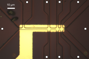
We investigate two QSHI devices of different crystallographic orientation and QW thickness, . In device D1, the QW with resides in a (013) plane, while the device D2 is based on the (112) QW with . We note that the QWs of both devices are similar in design to the QWs studied in Gusev et al. (2013); Olshanetsky et al. (2015). Both devices are shaped as multi-terminal Hall bars with Ti/Au metallic top gates, see insets of Fig. 1a and Fig. 1b for the schematic representation of the device and measurement configuration. The microscope image of one of the devices may be found in Supplemental Material Fig. 1. For additional device fabrication and measurement technique details see corresponding sections of Supplemental Material.
Using the gate voltage , the Fermi level can be tuned within the bulk energy gap, as large as in D1 and in D2 Bernevig et al. (2006); Olshanetsky et al. (2015). In this way the QSHI regime is realized, with the predominant edge conduction confirmed by transport measurements in similar devices Gusev et al. (2011); Tikhonov et al. (2015); Olshanetsky et al. (2015); Piatrusha et al. (2017) and, independently, here via non-local resistance measurements (see Supplemental Material Fig. 3). Various distances between the neighboring ohmic contacts allow us to choose the different lengths of the edge channels, spanning the range between and in each device, with edge resistance increasing with increasing edge length. The device D1 demonstrates resistance for the shortest edges, while in D2 the resistance is about twice as large for the same edge length (see Supplemental Material Figs. 9, 11). In the following we discuss the results obtained for device D1. Similar data obtained for device D2 is demonstrated in Supplemental Material.
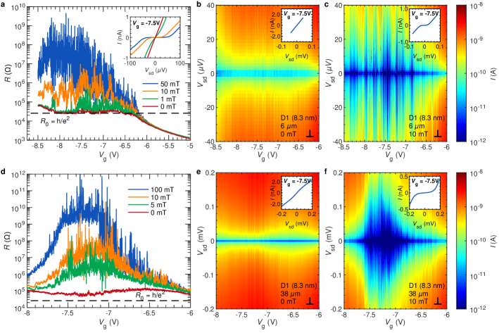
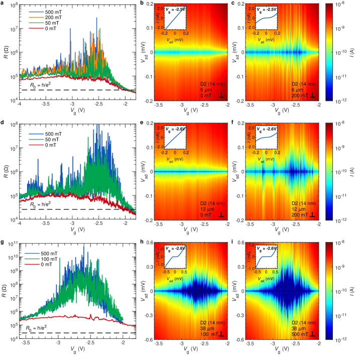
Figs. 1a and 1b show the two-terminal resistance of the and -long edges in D1, with subtracted contribution of contact terminals, as a function of in a magnetic field perpendicular to the QW plane, . The measurement configurations are shown in the corresponding insets. For the two-terminal resistance of an -terminal device in the phase-coherent case, Landauer-Buttiker analysis Büttiker (1988) would yield , which in our case is . This reasoning, however, is not applicable in our experiment since the edges longer than are in phase-incoherent regime.
For at , within the range of gate voltages the -long edge demonstrates the conductance plateau with the value close to and the device demonstrates the non-local resistance (see Supplemental Material Fig. 3), which corresponds to the onset of the QSHI regime. At the same time, no sizable -dependence is observed, which is usual for the QSHI edges Nowack et al. (2013); Gusev et al. (2014); Tikhonov et al. (2015). By contrast, in a small magnetic field of mT the resistance increases dramatically, sometimes reaching in mT at . Qualitatively similar but even stronger effect of the magnetic field is observed in the longer edge, as shown in Fig. 1b. As the temperature is raised to , the resistance drops down again by more than a factor of . The straightforward crosscheck demonstrates that in all our measurements the current flows along the edges of the device, while the bulk conduction contribution remains negligible even for (see Supplemental Material Fig. 4). All the edges of both our devices D1 and D2 exhibit the reported resistance increase in a small magnetic field which is also the case for the four-terminal configuration measurements (see Supplemental Material Figs. 9–12 for additional data).
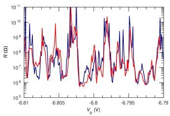
Figs. 1a and 1b highlight our main result that a tiny magnetic field gives rise to the dramatic increase of the resistance of the helical edge states accompanied by strong -dependence and highly reproducible, giant mesoscopic fluctuations (see Supplemental Material Fig. 5). Altogether, this behavior is a hallmark of the Anderson localization of the electronic states and manifests a transition from the topologically protected phase to the trivial insulator in a magnetic field as anticipated in various scenarios Durnev and Tarasenko (2016); Delplace et al. (2012); Raichev (2015). The underlying microscopic explanation is depicted in Fig. 1c. In , the dispersion relation of the helical electrons consists of two opposite spin counter-propagating branches, the coherent backscattering between which is forbidden by the topological protection Qi and Zhang (2011). In a finite -field, the branches hybridize, opening an energy gap in the vicinity of the Dirac point, and the spins of the counter-propagating electrons acquire a common tilt along the magnetic field. Thus, the coherent backscattering mediated by potential disorder is restored in the magnetic field, resulting in Anderson localization of the electronic states on the length-scale of the mean-free path, in contrast to the case.
It is important to emphasize that both short edges with and the longer ones with behave similarly in finite . Breaking the TRS with magnetic field allows coherent backscattering in both cases, leading to the helical edge states localization. In this scenario, the observation of for long edges in TRS-case is due to phase-breaking of the origin yet to be explained König et al. (2013); Ma et al. (2015); Xu and Moore (2006); Maciejko et al. (2009); Väyrynen et al. (2013); Kainaris et al. (2014); Wang et al. (2017); Väyrynen et al. (2018); Novelli et al. (2019), while the absence of localization in zero magnetic field for resistive edges manifests the topological protection.
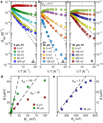
We now discuss in detail the -dependence of the QSH edge conductance under broken TRS. As seen from Fig. 2, in the absence of magnetic field the -dependence within the charge neutrality point (CNP) region is of metallic type with approximately change of the -long edge resistance as is reduced from to . For the -long edge, within the range of gate voltages we observe even stronger metallic behavior with a two fold decrease of resistance in the same interval. We are not aware of similar observations in HgTe QWs, where the reported -dependencies are usually either completely absent or weakly insulating. We note, however, that most of the studies discuss -dependencies at temperatures above . Additionally, we note that in D2, as well as for the -long edge in D1 within the range of gate voltages , the -dependence in is of weakly insulating type at any (see Supplemental Material Fig. 6).
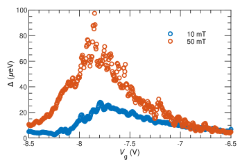
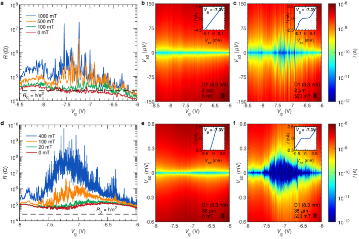
The -dependence in a magnetic field is much more impressive. In the presence of strong fluctuations, we analyze the log-averaged (typical) Beenakker (1997) conductance , with the averaging performed over the small gate-voltage region within the resistance maximum in Fig. 1b. This relatively narrow range of is chosen in order to resolve the fine structure of mesoscopic fluctuations in the vicinity of -value where the -dependence is prominent enough, as reflected by the gate voltage dependence of the activation energy (see Supplemental Material Fig. 8). The resulting data is shown in Fig. 2(a-c). Strikingly, already for mT the trend of changes from metallic to activated insulating dependence (the remnant -field did not exceed and was compensated in the experiment with precision). The activation energy reaches about in for the -long edge, shows a sub-linear increase with and increases with the length of the edge, Fig. 2d. Thus, it is difficult to make an obvious relation of the activated behavior with the single-particle spectrum of the helical edge states, e.g. with a Zeeman gap opening at the Dirac point. Similar observations hold for the in-plane orientation of the magnetic field, see Figs. 2(c,e) for the case of directed at about with respect to the edge under study. Here, the magnetic fields roughly an order of magnitude stronger are required to observe the activated behavior comparable to the case. This might be a consequence of the Lande -factor anisotropy predicted for HgTe QWs in some works Durnev and Tarasenko (2016).

We now quantitatively analyze the observed giant conductance fluctuations, which are the distinctive feature of the Anderson localized phase. Here, in contrast to the metallic phase, the conductance is exponentially sensitive to the minor variations of disorder, or equivalently, to the Fermi energy. As a result, the fluctuations of the conductance are as large as the average value and obey the log-normal distribution, i.e. it is the quantity which is Gaussian-distributed Beenakker (1997). In Fig. 3 we study the conductance fluctuations as a function of magnetic field at various . The square root of the normalized variance of the logarithm of the conductance, given by , is plotted in panels (a,b) for short and resistive edges in and in panel (c) for resistive edge in . At the lowest available it increases by more than one order of magnitude, compared to the case, for and . Still, the observed values are below the theoretical value of , which would correspond to a quantum-coherent Anderson localized phase Beenakker (1997). We attribute the difference to the impact of averaging in the presence of dephasing Xu and Moore (2006); Maciejko et al. (2009); Väyrynen et al. (2013); Kainaris et al. (2014); Wang et al. (2017); Väyrynen et al. (2018); Novelli et al. (2019), which also qualitatively explains the strong -dependence of the fluctuations in Fig. 3. The stronger fluctuations in the shorter edge further support this suggestion.
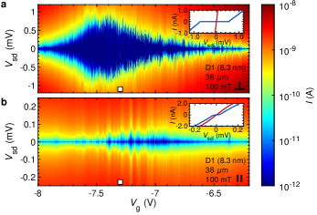
To further characterize the transport properties of the localized states, we study the non-linear transport regime originating from the delocalization of the edge states by the electric field Dolgopolov et al. (1992); Khavin et al. (1998) for the -long edge in D1 at . The dependence of on and is plotted in panels (a) and (b) of Fig. 4 for and , respectively. Within the CNP region one can see the dramatic changes in at increasing (note the log-scale). Below the certain threshold value of , which depends on with pronounced reproducible fluctuations above that, we observe only the negligible current through the edge. For the magnetic field of , the typical bias range of suppressed conduction changes from about in to about in . For this threshold, the corresponding energy scale is considerably higher than the activation energy extracted from the -dependencies similar to that of Fig. 2, indicating that the applied bias is shared among a few strongly localized electronic states along the edge. For the case of metal-insulator transition in Si inversion layers similar reasoning was suggested in Dolgopolov et al. (1992). Above the threshold, the conduction reasonably comparable to the case is restored. Two representative - cuts of Figs. 4a and 4b at are detailed in the corresponding insets, along with the - curves at . The observed highly non-linear transport behavior is yet another evidence of the Anderson localization of the helical states driven by the -field and contrasts with the almost linear current-voltage response in the TRS case (see Supplemental Material Figs. 4, 9–11).
In conclusion, through the low-temperature magnetoresistance measurements we were able to directly demonstrate the actual strength of topological protection in one-dimensional helical edge states of HgTe-based topological insulators. Breaking the TRS with an external magnetic field allowed us to expose the hallmark Anderson localization features for the edge states – the exponential -dependence, giant reproducible mesoscopic fluctuations and the gap-opening-like features in the - characteristics. Our observation of identical behavior of the edges independently of their resistance in the finite , strongly suggests the loss of topological protection at broken TRS. At the same time, the tremendous -dependence of the edges in , almost absent in zero , highlights the distinct action of TRS breaking compared to other mechanisms, which enable backscattering in . The observation of ballistic transport via helical edge states strongly depends on the material, it’s quality, may be even sample dependent and presently does not go beyond edges several micrometers long. Our experiment demonstrates that for resistive edges the topological protection is still there in the time-reversal symmetric case perfectly sustaining the edge transport from localization.
All the measurements were performed under the support of Russian Science Foundation Grant No. 18-72-10135. The high-resistance measurements were developed and tested within the state task of ISSP RAS. We thank I.V. Gornyi, T.M. Klapwijk, A.D. Mirlin, D.V. Shovkun and S.A. Tarasenko for helpful discussions.
References
- Bloch (1929) F. Bloch, Zeitschrift für Physik 52, 555 (1929).
- Kuga and Ishimaru (1984) Y. Kuga and A. Ishimaru, J. Opt. Soc. Am. A 1, 831 (1984).
- Albada and Lagendijk (1985) M. P. V. Albada and A. Lagendijk, Phys. Rev. Lett. 55, 2692 (1985).
- Wolf and Maret (1985) P.-E. Wolf and G. Maret, Phys. Rev. Lett. 55, 2696 (1985).
- Nazarov and Blanter (2009) Y. V. Nazarov and Y. M. Blanter, Quantum Transport: Introduction to Nanoscience (Cambridge University Press, 2009).
- Wiersma et al. (1997) D. S. Wiersma, P. Bartolini, A. Lagendijk, and R. Righini, Nature 390, 671 (1997).
- Schwartz et al. (2007) T. Schwartz, G. Bartal, S. Fishman, and M. Segev, Nature 446, 52 (2007).
- Lee and Ramakrishnan (1985) P. A. Lee and T. V. Ramakrishnan, Rev. Mod. Phys. 57, 287 (1985).
- Hu et al. (2008) H. Hu, A. Strybulevych, J. H. Page, S. E. Skipetrov, and B. A. van Tiggelen, Nature Physics 4, 945 (2008).
- Roati et al. (2008) G. Roati, C. D’Errico, L. Fallani, M. Fattori, C. Fort, M. Zaccanti, G. Modugno, M. Modugno, and M. Inguscio, Nature 453, 895 (2008).
- Billy et al. (2008) J. Billy, V. Josse, Z. Zuo, A. Bernard, B. Hambrecht, P. Lugan, D. Clément, L. Sanchez-Palencia, P. Bouyer, and A. Aspect, Nature 453, 891 (2008).
- Anderson (1958) P. W. Anderson, Phys. Rev. 109, 1492 (1958).
- Abrahams et al. (1979) E. Abrahams, P. W. Anderson, D. C. Licciardello, and T. V. Ramakrishnan, Phys. Rev. Lett. 42, 673 (1979).
- Hasan and Kane (2010) M. Z. Hasan and C. L. Kane, Rev. Mod. Phys. 82, 3045 (2010).
- Qi and Zhang (2011) X.-L. Qi and S.-C. Zhang, Rev. Mod. Phys. 83, 1057 (2011).
- Bernevig et al. (2006) B. A. Bernevig, T. L. Hughes, and S.-C. Zhang, Science 314, 1757 (2006).
- Konig et al. (2007) M. Konig, S. Wiedmann, C. Brune, A. Roth, H. Buhmann, L. W. Molenkamp, X.-L. Qi, and S.-C. Zhang, Science 318, 766 (2007).
- Knez et al. (2011) I. Knez, R.-R. Du, and G. Sullivan, Phys. Rev. Lett. 107, 136603 (2011).
- Olshanetsky et al. (2015) E. B. Olshanetsky, Z. D. Kvon, G. M. Gusev, A. D. Levin, O. E. Raichev, N. N. Mikhailov, and S. A. Dvoretsky, Phys. Rev. Lett. 114, 126802 (2015).
- Roth et al. (2009) A. Roth, C. Brune, H. Buhmann, L. W. Molenkamp, J. Maciejko, X.-L. Qi, and S.-C. Zhang, Science 325, 294 (2009).
- Suzuki et al. (2013) K. Suzuki, Y. Harada, K. Onomitsu, and K. Muraki, Phys. Rev. B 87, 235311 (2013).
- Li et al. (2017) T. Li, P. Wang, G. Sullivan, X. Lin, and R.-R. Du, Phys. Rev. B 96, 241406 (2017).
- Fei et al. (2017) Z. Fei, T. Palomaki, S. Wu, W. Zhao, X. Cai, B. Sun, P. Nguyen, J. Finney, X. Xu, and D. H. Cobden, Nature Physics 13, 677 (2017).
- Piatrusha et al. (2017) S. U. Piatrusha, V. S. Khrapai, Z. D. Kvon, N. N. Mikhailov, S. A. Dvoretsky, and E. S. Tikhonov, Phys. Rev. B 96, 245417 (2017).
- Gusev et al. (2013) G. M. Gusev, E. B. Olshanetsky, Z. D. Kvon, N. N. Mikhailov, and S. A. Dvoretsky, Phys. Rev. B 87, 081311 (2013).
- Brüne et al. (2012) C. Brüne, A. Roth, H. Buhmann, E. M. Hankiewicz, L. W. Molenkamp, J. Maciejko, X.-L. Qi, and S.-C. Zhang, Nature Physics 8, 485 (2012).
- Min’kov et al. (2015) G. M. Min’kov, A. A. Sherstobitov, A. V. Germanenko, O. E. Rut, S. A. Dvoretskii, and N. N. Mikhailov, JETP Letters 101, 469 (2015).
- Gusev et al. (2011) G. M. Gusev, Z. D. Kvon, O. A. Shegai, N. N. Mikhailov, S. A. Dvoretsky, and J. C. Portal, Phys. Rev. B 84, 121302 (2011).
- Nowack et al. (2013) K. C. Nowack, E. M. Spanton, M. Baenninger, M. König, J. R. Kirtley, B. Kalisky, C. Ames, P. Leubner, C. Brüne, H. Buhmann, L. W. Molenkamp, D. Goldhaber-Gordon, and K. A. Moler, Nature Materials 12, 787 (2013).
- Du et al. (2015) L. Du, I. Knez, G. Sullivan, and R.-R. Du, Phys. Rev. Lett. 114, 096802 (2015).
- Wu et al. (2018) S. Wu, V. Fatemi, Q. D. Gibson, K. Watanabe, T. Taniguchi, R. J. Cava, and P. Jarillo-Herrero, Science 359, 76 (2018).
- Bendias et al. (2018) K. Bendias, S. Shamim, O. Herrmann, A. Budewitz, P. Shekhar, P. Leubner, J. Kleinlein, E. Bocquillon, H. Buhmann, and L. W. Molenkamp, Nano Letters 18, 4831 (2018), pMID: 29975844.
- de Picciotto et al. (2001) R. de Picciotto, H. L. Stormer, L. N. Pfeiffer, K. W. Baldwin, and K. W. West, Nature 411, 51 (2001).
- Gusev et al. (2014) G. M. Gusev, Z. D. Kvon, E. B. Olshanetsky, A. D. Levin, Y. Krupko, J. C. Portal, N. N. Mikhailov, and S. A. Dvoretsky, Phys. Rev. B 89, 125305 (2014).
- Tikhonov et al. (2015) E. S. Tikhonov, D. V. Shovkun, V. S. Khrapai, Z. D. Kvon, N. N. Mikhailov, and S. A. Dvoretsky, JETP Letters 101, 708 (2015).
- Aseev and Nagaev (2016) P. P. Aseev and K. E. Nagaev, Phys. Rev. B 94, 045425 (2016).
- Piatrusha et al. (2018) S. U. Piatrusha, L. V. Ginzburg, E. S. Tikhonov, D. V. Shovkun, G. Koblmüller, A. V. Bubis, A. K. Grebenko, A. G. Nasibulin, and V. S. Khrapai, JETP Letters 108, 71 (2018).
- Qian et al. (2014) X. Qian, J. Liu, L. Fu, and J. Li, Science 346, 1344 (2014).
- Fu and Kane (2008) L. Fu and C. L. Kane, Phys. Rev. Lett. 100, 096407 (2008).
- Xu and Moore (2006) C. Xu and J. E. Moore, Phys. Rev. B 73, 045322 (2006).
- Maciejko et al. (2009) J. Maciejko, C. Liu, Y. Oreg, X.-L. Qi, C. Wu, and S.-C. Zhang, Phys. Rev. Lett. 102, 256803 (2009).
- Väyrynen et al. (2013) J. I. Väyrynen, M. Goldstein, and L. I. Glazman, Phys. Rev. Lett. 110, 216402 (2013).
- Kainaris et al. (2014) N. Kainaris, I. V. Gornyi, S. T. Carr, and A. D. Mirlin, Phys. Rev. B 90, 075118 (2014).
- Wang et al. (2017) J. Wang, Y. Meir, and Y. Gefen, Phys. Rev. Lett. 118, 046801 (2017).
- Väyrynen et al. (2018) J. I. Väyrynen, D. I. Pikulin, and J. Alicea, Phys. Rev. Lett. 121, 106601 (2018).
- Novelli et al. (2019) P. Novelli, F. Taddei, A. K. Geim, and M. Polini, Phys. Rev. Lett. 122, 016601 (2019).
- Durnev and Tarasenko (2016) M. V. Durnev and S. A. Tarasenko, Phys. Rev. B 93, 075434 (2016).
- Büttiker (1988) M. Büttiker, Phys. Rev. B 38, 9375 (1988).
- Delplace et al. (2012) P. Delplace, J. Li, and M. Büttiker, Phys. Rev. Lett. 109, 246803 (2012).
- Raichev (2015) O. Raichev, Ukrainian Journal of Physics 60, 538 (2015).
- König et al. (2013) M. König, M. Baenninger, A. G. F. Garcia, N. Harjee, B. L. Pruitt, C. Ames, P. Leubner, C. Brüne, H. Buhmann, L. W. Molenkamp, and D. Goldhaber-Gordon, Phys. Rev. X 3, 021003 (2013).
- Ma et al. (2015) E. Y. Ma, M. R. Calvo, J. Wang, B. Lian, M. Muhlbauer, C. Brune, Y. T. Cui, K. Lai, W. Kundhikanjana, Y. Yang, M. Baenninger, M. Konig, C. Ames, H. Buhmann, P. Leubner, L. W. Molenkamp, S. C. Zhang, D. Goldhaber-Gordon, M. A. Kelly, and Z. X. Shen, Nature Communications 6, 7252 (2015).
- Beenakker (1997) C. W. J. Beenakker, Rev. Mod. Phys. 69, 731 (1997).
- Dolgopolov et al. (1992) V. T. Dolgopolov, G. V. Kravchenko, A. A. Shashkin, and S. V. Kravchenko, Phys. Rev. B 46, 13303 (1992).
- Khavin et al. (1998) Y. B. Khavin, M. E. Gershenson, and A. L. Bogdanov, Phys. Rev. B 58, 8009 (1998).
Supplemental Material
Device fabrication
The single HgTe QWs as heterojunction were grown by molecular beam epitaxy on SI GaAs substrates with buffer ZnTe and CdTe layers CdTe with the thickness of and -, respectively. The mesa was fabricated via plasma chemical etching followed by covering with insulating layers, thick in total. All devices are equipped with evaporated Au/Ti metallic gates.
Measurement techniques
All devices were measured in a BlueFors-LD dilution refrigerator with a base temperature of equipped with a superconducting solenoid. The lowest obtainable electronic temperature was , verified by the Johnson-Nyquist thermometry. The two-terminal linear response resistances were obtained by differentiating of the - curves, measured via the transimpedance amplifier with coefficient – see Supplemental Material Fig. 2. For all the data we subtract the contact resistance which was determined separately and typically ranged between and for each terminal in our devices. Presenting the data, we also do not take into account the parallel conduction channel which appears in the QSHI regime and which is due to transport in the counterdirection for a given edge. This parallel channel would lead to the correction of approximately for the -long edge in D1 and of approximately for the -long edge in D2 in zero magnetic field. It is harder to estimate the correction in the finite due to the absence of self-averaging of resistance of the edge channels in the insulating regime.


