An integrated low-voltage broadband lithium niobate phase modulator
Abstract
Electro-optic phase modulators are critical components in modern communication, microwave photonic, and quantum photonic systems. Important for these applications is to achieve modulators with low half-wave voltage at high frequencies. Here we demonstrate an integrated phase modulator, based on a thin-film lithium niobate platform, that simultaneously features small on-chip loss ( 1 dB) and low half-wave voltage over a large spectral range (3.5 - 4.5 V at 5 - 40 GHz). By driving the modulator with a strong 30-GHz microwave signal corresponding to around four half-wave voltages, we generate an optical frequency comb consisting of over 40 sidebands spanning 10 nm in the telecom L-band. The high electro-optic performance combined with the high RF power-handling ability (3.1 W) of our integrated phase modulator are crucial for future photonics and microwave systems.
Electro-optic (EO) phase modulators are fundamental building blocks in photonics and microwave systems. Possible applications include photonic radio-frequency (RF) front ends for radio-over-fiber systems Clark and Waterhouse (2011), telecommunication systems Janner et al. (2009); Miller (2017); Wang et al. (2018a); Wooten et al. (2000), EO frequency combs Zhang et al. (2018), temporal imaging systems Kolner (1994) and quantum photonics Kues et al. (2017). Among various material platforms explored, including Si Dong et al. (2009), InP Li et al. (2010), AlN Xiong et al. (2012), plasmonics Melikyan et al. (2014), graphene Mohsin et al. (2015) and polymers Lee et al. (2002), lithium niobate (LN) has been the most widely used for high-end phase modulator applications. This is due to LN’s outstanding material properties, including good temperature stability, wide transparency window and most importantly highly efficient linear EO (Pockels) effect Wooten et al. (2000); Arizmendi (2004); Boes et al. (2018). Commercially available LN phase modulators today are generally based on bulk LN crystals, where a weak optical index contrast is created by ion in-diffusion or proton exchange technologies Bazzan and Sada (2015). The low index contrast results in low optical confinement and high half-wave voltage (Vπ), the latter of which is defined as the voltage required to switch the phase of light by 180∘. For example, the Vπ of a typical commercial phase modulator operating at 1525 - 1605 nm is 7.5 V at 30 GHz Thorlabs .
Thin-film lithium niobate on insulator (LNOI) platform Boes et al. (2018); Poberaj et al. (2012) has recently emerged as a promising approach to realize integrated EO modulators with stronger optical confinement and high EO efficiencies while occupying a smaller footprint Wang et al. (2018a); Cai et al. (2016); Stenger et al. (2018); Rao et al. (2016); Jin et al. (2016); Macario et al. (2012); Mercante et al. (2016); Weigel et al. (2018). For example, LNOI phase modulators with relatively low Vπ (3.8 V at DC) have been demonstrated Mercante et al. (2016), albeit at the expense of a high on-chip optical loss of 10.5 dB.
Here we demonstrate a dual channel phase modulator (Fig. 1) using a thin-film LNOI platform with low on-chip optical loss ( 1 dB/channel) and low RF Vπ (4.5 V at 40 GHz) that is relatively constant (less than 28% variation) over wide frequency range (from 5 to 40 GHz). The low RF Vπ, high RF power-handling capability and low optical losses together allow us to generate an EO frequency comb with over 40 sidebands using a single modulator, instead of cascading multiple devices Papp et al. (2014).
We first fabricate the optical waveguide using electron-beam lithography (EBL) followed by reactive-ion etching with argon (Ar+) ions Zhang et al. (2017); Wang et al. (2018a). Next, gold RF electrodes with spatial separation of 5 m are placed along the waveguides. In contrast to our previous work Wang et al. (2018a), where a second EBL was used to define the electrodes, here we use direct-write laser lithography (Heidelberg MLA150). This allows us to pattern the electrodes more than 30 times faster than EBL, while maintaining a good alignment accuracy.
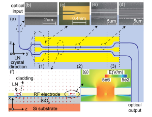
In order to achieve low RF Vπ values and high optical bandwidths, a 50- impedance-matched traveling-wave RF transmission line is used, where the optical and RF group velocities are matched Wang et al. (2018a). To achieve this, we employ coplanar waveguide geometry with ground-signal-ground (GSG) configuration, where the electric fields in the two gaps have opposite directions (Fig. 1). The input and output sections are designed to have wider signal lines for RF probes contacting purposes, since the 30-m-wide signal line in the modulation section is too narrow for electrical probes. The optical signal is equally split into two paths, which are modulated separately. The push-pull phase modulator design is of interest for fiber-optic gyroscopes where differential phase shift can be useful Huang et al. (1993) and phase-modulated optical links Urick et al. (2015). For other applications the Y-splitter can be removed to reduce the associated 3 dB loss. Our numerical modeling indicates that the majority of the electric field is focused around the gap area (Fig. 1(f) and Fig. 1(g)), indicating a good overlap between optical and microwave fields. The microwave electrodes are placed such that the major field component is aligned with the direction of our x-cut LN crystal (Fig. 1) in order to make use of the strongest EO coefficient Wooten et al. (2000). The strong optical confinement in our structures (index contrast 0.67) allows for a small electrode-waveguide gap (5 m) resulting in a high EO modulation efficiency. The rib waveguide has a top width of 700 nm, which allows single-mode operation for transverse-electric (TE) polarization Wang et al. (2018b). The total thickness of the LN layer is 600 nm, with top 300 nm etched to form the rib waveguide. The high-quality etching is confirmed by a scanning electron microscope (SEM) examination before cladding (Fig. 1(b)), showing smooth sidewalls of the optical waveguide.
Longer metal electrodes are preferred for minimizing the driving power (and voltage) since they can induce more phase shift at a given driving voltage. In practice, however, longer electrodes result in higher microwave losses, which reduces the bandwidth of the phase modulator. Moreover, minor misalignment in the electrode fabrication (visible in Fig. 1(d) and Fig. 1(e)) can result in optical absorption due to adjacent metal electrodes. Here, we choose a trade-off with the modulation section length being 2 cm long (Fig. 1(a)). To reduce the microwave transmission losses, electrodes thickness should be larger than the skin depth at the frequency of interest. We fabricate 1.6-m thick microwave electrodes, using a gold evaporation process, which is about 1.5 times the skin depth at 5 GHz and about 4 times the skin depth at 40 GHz.
To characterize the modulators, light from a tunable telecom laser (Santec TSL-510) is launched into the device using a lensed fiber (OZoptics). The transmitted light is collected using another lensed fiber and detected using an InGaAs photodetector (New focus 1811). The overall transmission loss from the input fiber to one of the output fibers is measured to be 16.9 dB, with 3 dB originating from the Y-splitter. The remaining 13.9 dB loss is largely due to input and output coupling losses at chip facets, which is measured to be 60.5 dB/facet. This is accomplished using a cut-back method by comparing the insertion losses of several devices with similar waveguide geometry but different total lengths. The coupling loss could be reduced by employing mode-converters, such as tapered waveguides, to improve the overlap between the fiber and waveguide modes Mitomi et al. (1994). Finally, we estimate the total on-chip loss including the splitter to be 4 dB and the waveguide propagation loss to be 1 dB, which is comparable with our previous work Wang et al. (2018a). The small waveguide propagation loss allows advanced architectures such as cascaded modulators to be added without induce a large increase in insertion loss Otsuji et al. (1996).
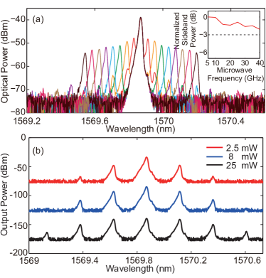
One of the most useful figures of merit for EO phase modulators is the frequency dependency of RF Vπ Gopalakrishnan et al. (1994). We measure it by driving our phase modulator using sinusoidal electrical signals from an RF signal generator (Hittite HMC-T2240, 0 to 40 GHz). The modulated optical signal is analyzed by an optical spectrum analyzer (OSA) (Yokogawa AQ6370). Fig. 2 (a) shows the measured spectra when driving the modulator at RF frequencies from 5 GHz to 40 GHz, where a pair of symmetrical sidebands are generated in the frequency domain Kawanishi et al. (2007); Shi et al. (2003). We note that reflections between the end-facets of the waveguide give rise to residual intensity modulation of 6% (of total transmitted optical power). This was measured by driving a modulator with a 100-kHz triangular wave with a voltage exceeding Vπ. This intensity modulation, however quickly drops off at GHz frequencies due to the lifetime ( 300 ps) of the Faber-Perot resonance formed between the waveguide facets and velocity mismatch between the RF signal and the resonant standing wave. Therefore, we conclude that sideband generation that we observe is mostly due the phase modulation. RF signals below 5 GHz are not measured since the generated sidebands could not be well separated from the carrier light, due to the limited spectral resolution of the OSA. The EO roll-off of the first sidebands is estimated to be 2.1 dB in the 5 to 40 GHz range. This value was obtained by subtracting the RF cable losses (inset of Fig. 2(a)) from the measured data, indicating a flat frequency response of RF Vπ over a wide frequency range. For increased RF driving powers, high-order sidebands are generated (Fig. 2(b)).
The power ratio between the modulated sidebands and the carrier band from the measured spectra can be used to determine RF Vπ at any given frequency. In particular, the powers in the carrier band and the generated sidebands are related via the Bessel function, based on which, we can evaluate the RF Vπ values using
| (1) |
where is peak-to-peak drive voltage, is the power of the RF signal, is the impedance of driving circuit, and is the measured modulation amplitude, which is the phase change (zero-to-peak) of the phase modulator Kawanishi et al. (2007); Shi et al. (2003). Fig. 3 shows the extracted RF Vπ values at different frequencies. We find that RF only increases slowly, ranging between 3.5 V to 4.5 V in the range of 5 to 40 GHz, which corresponds to an increase of only 28% over a very broad spectral range. The relative EO roll-off is 2.2 dB, which is consistent with the roll-off calculated from the first sidebands powers (Fig. 2(a)).
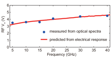
We further confirm the measured EO roll-off by calculating the RF Vπ values from the measured electrical responses (transmission coefficient, ) of the RF electrodes. Assuming perfect velocity matching between RF and optical fields, the dominant origin of EO roll-off arises from the performances of the RF transmission line. The extracted RF Vπ using this method is in excellent agreement with the optical measurement (Fig. 3), confirming that the RF and optical velocities are well matched. Note that all Vπ values cited in this work correspond to a -phase shift in a single optical path, therefore being roughly twice compared with the Mach-Zehnder interferometer architecture which can employ a push-pull configuration Wang et al. (2018a).
In general, Vπ is directly proportional to the width of the gap and inversely proportional to the length of the electrode. Therefore, smaller gaps and longer electrodes will give rise to a lower Vπ. However, reduced electrode gap increases optical loss due to metal absorption, while longer electrodes contribute to larger microwave loss, and smaller bandwidth. Importantly, even with this trade-off taken into account, our modulator’s performance exceeds that of the commercial counterparts in both optical losses and Vπ with an overall shorter device length due to the high confinement of the optical mode Thorlabs ; eospace ; iXblue . Moreover, our RF Vπ is also flat over a large frequency band due to the reduced metal electrode length.
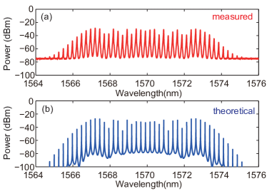
One particularly important application of phase modulators is EO comb generation, which is of interest for telecommunication Kippenberg et al. (2011); Zhang et al. (2018), ultra-fast optics Gohle et al. (2005), and so on. The main challenge to realize this is the requirement of a low RF Vπ and high RF power handling ability. For this reason, past realizations of EO combs by a single phase modulator are relatively narrow Sakamoto et al. (2006). Alternative configurations that can generate broader combs use multiple modulators (commonly three or four) Papp et al. (2014), which requires multiple high power RF drives and introduces additional optical insertion loss. Due to the low RF Vπ of our phase modulator, we are able to generate a broad EO comb with over 40 spectral lines spanning 10 nm in frequency domain, with a single phase modulator. This is accomplished by driving the modulator by a 30 GHz RF signal amplified to 3.1 W, corresponding to a total acquired phase shift of 4. The measured optical spectrum (Fig. 4(a)) is in good agreement with the theoretical prediction (Fig. 4(b)) further confirming the capability of our devices to handle high RF powers without introducing significant signal distortions. For comparison, using modeling we estimate that the same RF power applied to a commercial phase modulator (model LN27S-FC with Vπ of 7.5 V at 30 GHz) Thorlabs would result in 6 nm wide comb, with 28 lines. This clearly illustrates the positive role of lower Vπ on EO comb bandwidth.
In conclusion, we have demonstrated a high-performance phase modulator based on LNOI platform, featuring low on-chip optical losses and low half-wave voltages. The measured RF Vπ values remain relatively constant over a broad frequency range. The flatness of the frequency response indicates that the device could also perform well at very high frequencies exceeding 100 GHz Wang et al. (2018a); Mercante et al. (2018), showing high potential for millimeter-wave and terahertz applications. Further reducing the electrode gap and the RF loss could lead to even lower RF Vπ and broader EO combs. Many phase modulator applications require the modulators to be driven at voltages far exceeding the half-wave voltage Wooten et al. (2000). These applications are consequently limited by the required high voltages and low power-handling ability, which we overcome with the here-presented modulators. Our work shows that phase modulators made from thin-film LN outperform conventional bulk modulators simultaneously in half-wave voltage, optical propagation loss, size and EO bandwidth. Our work therefore enables new ventures in EO signal processing, as well as microwave and terahertz photonics.
We acknowledge Collins Aerospace, National Science Foundation (NSF) (ECCS-1740296), DARPA SCOUT program (W31P4Q-15-1-0013) and City University of Hong Kong (Start-up Funds) for partly funding this research. We thank R. Morandotti for providing an RF amplifier. Device fabrication was performed at the center for nanoscale systems (CNS) at Harvard University (1541959).
References
- Clark and Waterhouse (2011) T. R. Clark and R. Waterhouse, IEEE microwave magazine 12, 87 (2011).
- Janner et al. (2009) D. Janner, D. Tulli, M. García‐Granda, M. Belmonte, and V. Pruneri, Laser & Photonics Reviews 3, 301 (2009).
- Miller (2017) D. A. Miller, Journal of Lightwave Technology 35, 346 (2017).
- Wang et al. (2018a) C. Wang, M. Zhang, X. Chen, M. Bertrand, A. Shams-Ansari, S. Chandrasekhar, P. Winzer, and M. Lončar, Nature , 1 (2018a).
- Wooten et al. (2000) E. L. Wooten, K. M. Kissa, A. Yi-Yan, E. J. Murphy, D. A. Lafaw, P. F. Hallemeier, D. Maack, D. V. Attanasio, D. J. Fritz, and G. J. McBrien, IEEE Journal of selected topics in Quantum Electronics 6, 69 (2000).
- Zhang et al. (2018) M. Zhang, B. Buscaino, C. Wang, A. Shams-Ansari, C. Reimer, R. Zhu, J. Kahn, and M. Loncar, arXiv preprint arXiv:1809.08636 (2018).
- Kolner (1994) B. H. Kolner, IEEE Journal of Quantum Electronics 30, 1951 (1994).
- Kues et al. (2017) M. Kues, C. Reimer, P. Roztocki, L. R. Cortés, S. Sciara, B. Wetzel, Y. Zhang, A. Cino, S. T. Chu, and B. E. Little, Nature 546, 622 (2017).
- Dong et al. (2009) P. Dong, S. Liao, D. Feng, H. Liang, D. Zheng, R. Shafiiha, C.-C. Kung, W. Qian, G. Li, and X. Zheng, Optics express 17, 22484 (2009).
- Li et al. (2010) Y. Li, R. Wang, A. Bhardwaj, S. Ristic, and J. Bowers, IEEE Photonics Technology Letters 22, 1340 (2010).
- Xiong et al. (2012) C. Xiong, W. H. Pernice, X. Sun, C. Schuck, K. Y. Fong, and H. X. Tang, New Journal of Physics 14, 095014 (2012).
- Melikyan et al. (2014) A. Melikyan, L. Alloatti, A. Muslija, D. Hillerkuss, P. C. Schindler, J. Li, R. Palmer, D. Korn, S. Muehlbrandt, and D. Van Thourhout, Nature Photonics 8, 229 (2014).
- Mohsin et al. (2015) M. Mohsin, D. Neumaier, D. Schall, M. Otto, C. Matheisen, A. L. Giesecke, A. A. Sagade, and H. Kurz, Scientific reports 5, 10967 (2015).
- Lee et al. (2002) M. Lee, H. E. Katz, C. Erben, D. M. Gill, P. Gopalan, J. D. Heber, and D. J. McGee, Science 298, 1401 (2002).
- Arizmendi (2004) L. Arizmendi, physica status solidi (a) 201, 253 (2004).
- Boes et al. (2018) A. Boes, B. Corcoran, L. Chang, J. Bowers, and A. Mitchell, Laser & Photonics Reviews 12, 1700256 (2018).
- Bazzan and Sada (2015) M. Bazzan and C. Sada, Applied Physics Reviews 2, 040603 (2015).
- (18) Thorlabs, “40 GHz Phase Modulator without Polarizer, FC/PC Connectors,” .
- Poberaj et al. (2012) G. Poberaj, H. Hu, W. Sohler, and P. Guenter, Laser & Photonics Reviews 6, 488 (2012).
- Cai et al. (2016) L. Cai, Y. Kang, and H. Hu, Optics express 24, 4640 (2016).
- Stenger et al. (2018) V. Stenger, J. Toney, D. Brown, S. McKeown, B. Griffin, R. Nelson, and S. Sriram (IEEE, 2018) pp. 1–3.
- Rao et al. (2016) A. Rao, A. Patil, P. Rabiei, A. Honardoost, R. DeSalvo, A. Paolella, and S. Fathpour, Optics letters 41, 5700 (2016).
- Jin et al. (2016) S. Jin, L. Xu, H. Zhang, and Y. Li, IEEE Photonics Technology Letters 28, 736 (2016).
- Macario et al. (2012) J. Macario, P. Yao, S. Shi, A. Zablocki, C. Harrity, R. D. Martin, C. A. Schuetz, and D. W. Prather, Optics express 20, 23623 (2012).
- Mercante et al. (2016) A. J. Mercante, D. L. Eng, M. Konkol, P. Yao, S. Shi, and D. W. Prather, Optics letters 41, 867 (2016).
- Weigel et al. (2018) P. O. Weigel, J. Zhao, K. Fang, H. Al-Rubaye, D. Trotter, D. Hood, J. Mudrick, C. Dallo, A. T. Pomerene, A. L. Starbuck, C. T. DeRose, A. L. Lentine, G. Rebeiz, and S. Mookherjea, arXiv preprint arXiv:1803.10365 (2018).
- Papp et al. (2014) S. B. Papp, K. Beha, P. Del’Haye, F. Quinlan, H. Lee, K. J. Vahala, and S. A. Diddams, Optica 1, 10 (2014).
- Zhang et al. (2017) M. Zhang, C. Wang, R. Cheng, A. Shams-Ansari, and M. Lončar, Optica 4, 1536 (2017).
- Huang et al. (1993) S. Y. Huang, K. Toyama, P.-A. Nicati, L. Thevenaz, B. Y. Kim, and H. J. Shaw (International Society for Optics and Photonics, 1993) pp. 48–60.
- Urick et al. (2015) V. J. Urick, K. J. Williams, and J. D. McKinney, Fundamentals of microwave photonics (John Wiley & Sons, 2015).
- Wang et al. (2018b) C. Wang, M. Zhang, B. Stern, M. Lipson, and M. Lončar, Optics express 26, 1547 (2018b).
- Mitomi et al. (1994) O. Mitomi, K. Kasaya, and H. Miyazawa, IEEE Journal of Quantum Electronics 30, 1787 (1994).
- Otsuji et al. (1996) T. Otsuji, M. Yaita, T. Nagatsuma, and E. Sano, IEEE Journal of selected topics in Quantum Electronics 2, 643 (1996).
- Gopalakrishnan et al. (1994) G. K. Gopalakrishnan, W. K. Burns, R. W. McElhanon, C. H. Bulmer, and A. S. Greenblatt, Journal of Lightwave Technology 12, 1807 (1994).
- Kawanishi et al. (2007) T. Kawanishi, T. Sakamoto, and M. Izutsu, IEEE Journal of selected topics in Quantum Electronics 13, 79 (2007).
- Shi et al. (2003) Y. Shi, L. Yan, and A. E. Willner, Journal of Lightwave Technology 21, 2358 (2003).
- (37) eospace, “A low-loss and wideband phase modulator for chirp control or coherent optical applications,” .
- (38) iXblue, “Lithium Niobate Electro Optic Modulator MPZ-LN-40,” .
- Kippenberg et al. (2011) T. J. Kippenberg, R. Holzwarth, and S. A. Diddams, Science 332, 555 (2011).
- Gohle et al. (2005) C. Gohle, T. Udem, M. Herrmann, J. Rauschenberger, R. Holzwarth, H. A. Schuessler, F. Krausz, and T. W. Hänsch, Nature 436, 234 (2005).
- Sakamoto et al. (2006) T. Sakamoto, T. Kawanishi, and M. Izutsu, Optics letters 31, 811 (2006).
- Mercante et al. (2018) A. J. Mercante, S. Shi, P. Yao, L. Xie, R. M. Weikle, and D. W. Prather, Optics express 26, 14810 (2018).