In situ analysis of catalyst composition during gold catalyzed GaAs nanowire growth
Abstract
Semiconductor nanowires offer the opportunity to incorporate novel structures and functionality into electronic and optoelectronic devices. A clear understanding of the nanowire growth mechanism is essential for well-controlled growth of structures with desired properties, but the understanding is currently limited by a lack of empirical measurements of important parameters during growth, such as catalyst particle composition. However, this is difficult to accurately determine by investigating post-growth. We report direct measurement of the catalyst composition of individual gold seeded GaAs nanowires inside an electron microscope as they grow. The Ga content in the catalyst during growth increased with both temperature and Ga precursor flux. A direct comparison of the calculated phase diagrams of the Au-Ga-As ternary system to the measured catalyst composition not only lets us estimate the As content in the catalyst but also indicates the relevance of phase diagrams to understanding nanowire growth.
keywords:
Catalyst composition, GaAs, nanowire, in situ growthIntroduction
Nanowire growth by the vapor-liquid-solid (VLS) method is an important technique for producing well-controlled nanocrystals suitable for quantum components. For III-V semiconductors, an important materials system for future technologies within electronics, solid-state lighting and quantum processing, VLS growth enables the fabrication of, for example, lattice-mismatched heterostructures,[1, 2, 3] metastable crystal phases and crystal phase tuning,[4, 5, 6, 7] and unusual ternary alloys[8, 9]. VLS growth has been well-studied for over two decades, and extensive theoretical efforts exist to explain the growth process itself,[10, 11, 12, 13, 14] the observed trends with experimental parameters,[15, 16, 17, 18] and the existence of metastable structures[19, 20, 21]. However, validation of theoretical predictions remains extremely difficult due to the large number of variable material properties and accessible experimental parameters, and the subsequent variance in reported experimental trends. Additionally, many of the important fundamental parameters, such as surface and interface energies for relevant growth conditions, are unknown.[22, 23] Consequently, there are a wide range of competing and complementary models that can explain observations such as crystal phase trends[6, 24, 25, 26] and diameter-growth rate dependencies[27, 28, 29, 30, 31, 32].
The use of in situ characterization methods to gain direct insights into semiconductor nanowire growth in real time is one of the most effective ways to refine theoretical explanations and predictions, and in turn to better understand the conditions needed to design these materials with high control.[33] Examples of previous in situ studies include X-ray diffraction to understand phase and structural evolution,[34, 35, 36] infrared spectroscopy to correlate surface chemistry during growth with resulting nanowire morphology,[37, 38, 39] reflectance high-energy electron diffraction to follow nucleation and structural changes,[40, 41, 42] optical reflectometry to monitor growth rate evolution,[43, 44] and mass spectrometry to study nucleation[45]. In addition, in situ scanning electron microscopy has been used to directly follow nanowire growth and morphology, and combined with Auger electron spectroscopy to track surface chemistry.[46] Finally, in situ transmission electron microscopy (TEM) has proven to be one of the most powerful ways to gain insight into nanowire growth in a directly interpretable way. Importantly, the information provided by this method is local, meaning that the nanowire, the growth-enabling liquid droplet and the interface between them can be visually identified and independently studied. This method has led to numerous significant breakthroughs in nanowire growth such as vapor-solid-solid growth,[47, 48] corner truncation,[49, 50] and step-flow[48]. In situ TEM studies have been particularly beneficial for understanding bilayer growth kinetics,[51] crystal phase switching,[52] triple-phase-line nucleation,[53] and double bilayer growth[54] in III-V nanowires.
One essential thing that remains to be investigated is the local composition of the nanostructure during growth. This is necessary to understand composition evolution in for instance heterostructure and ternary nanowires, but even more importantly, it is necessary for understanding the composition of the liquid metal droplet as a function of growth parameters and how this is correlated with the resulting nanowire properties.[55] The composition of the catalyst particle is a pivotal factor that determines its thermodynamic parameters such as vapor pressure, chemical potential and surface energies which in turn decide the nanowire structure, growth rate, composition etc.[56, 57, 58]. So far, the composition of the catalyst particles have been measured post-growth and was shown to depend on the conditions used for terminating the growth[59, 60] (more details in Supplementary Information section S1), implying that post-growth composition of the particle is different from its composition during growth. To our knowledge, there has been no direct in situ measurement of catalyst composition during nanowire growth. An indirect estimation of the Au-Ga catalyst composition during GaAs nanowire growth has been reported by comparing the dimensions of the starting Au seeds particles and the catalyst during growth by assuming that the seed material does not diffuse out of the catalyst particle.[52] By comparing the catalyst composition measured in situ with calculated phase diagram one can also investigate the validity of using equilibrium phase diagrams in understanding the non-equilibrium nanowire growth. In nanowire growth models which consider phase diagrams, the nanowire growth is assumed to happen when the composition exceeds the liquidus line along which the nanowire material coexists in equilibrium with a stable liquid catalyst alloy.[61]
In this article we report for the first time direct in situ measurement of catalyst composition during nanowire growth. We use in situ X-ray energy dispersive spectroscopy (XEDS) combined with in situ TEM to investigate the composition of the metal droplet as a function of growth parameters for Au-seeded GaAs nanowires grown by the VLS method. We show that the droplet consists of a significant quantity of Ga for all growth conditions, which increases with temperature for constant precursor flow. We do not observe any As significantly above the detection limit of the XEDS technique. Using calculated ternary phase diagrams, we show that the As content can however be estimated based on the temperature dependence of the Ga content. We also observe that the Ga content of the droplet for a given temperature is relatively independent of the ratio of V/III precursor species, so long as this ratio is above a certain threshold. Below this threshold, the Ga content increases strongly with decreasing V/III ratio, accompanied by a volume increase in the droplet. We show that the droplet volume scales with the Ga content, validating earlier works that used volume as an estimate of Ga.[52] The trend with V/III ratio is understood to correlate with a gradual transition towards the so-called ´´arsenic-limited´´ growth, whereby the droplet initially swells up but eventually stabilizes.[62] The results demonstrate that in situ XEDS is a useful and direct way to gain important insight and information on nanowire growth in real time, and will be similarly appropriate for other types of processes occurring at similar temperatures and overall gas pressures. Finally, the measurements of the droplet composition as a function of growth parameters will provide important inputs to validation and modification of theoretical models describing nanowire growth.[14, 55, 63]
Results and discussion
Growth of GaAs nanowires and in situ measurements
Au nanoparticles deposited on a silicon nitride-based heating grid were used to seed the nanowire growth. Nanowires were grown inside a Hitachi HF3300S environmental TEM integrated with a custom metal organic chemical vapor deposition (MOCVD) system. Trimethylgallium (TMGa) and arsine (AsH3), which are the most common precursor gases in MOCVD growth of GaAs, were used for this study. The chemical composition of the catalyst was studied by XEDS as a function of temperature and the ratio of precursor fluxes, which are two very important parameters in typical MOCVD-growth. Please refer to Methods section for more details.
XEDS of catalyst measured in situ
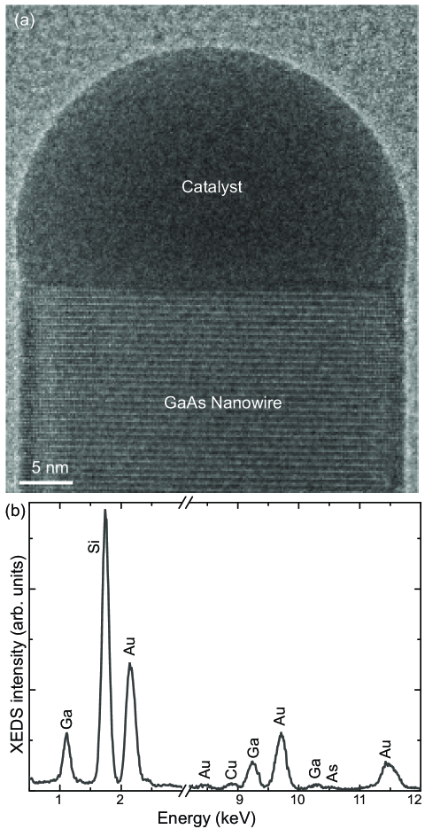
The catalyst composition was measured using XEDS in situ as the GaAs nanowire grows. An example XEDS spectrum is shown in Fig. 1 (b) from the nanowire shown in Fig. 1 (a). Clear signals from Ga and Au in the catalyst are observed for all spectra, along with a strong Si signal arising from the SiNx grid on which the nanowires are growing, and system artefacts such as Cu arising from microscope components. Quantification of the XEDS spectrum in Fig. 1 (b), measured at 440 ∘C, gives a Ga:Au atomic ratio of about 30:70 (assuming only Ga and Au are present). Some spectra also show small features that could be due to As, but the quantity is too low to be conclusively attributed to As and quantified (further information is available in the Methods section). Since any As within the catalyst is too low to be directly quantified, we can only put an upper limit on the As content (of approximately 1-2 atomic %). Our observation of very low concentration of As in the catalyst during growth is consistent with theoretical calculations; for instance, Glas et al. calculate the As content to be about 1 % (depending on radius and contact angle).[64] Mårtensson et al. predicted As content to be roughly in the range 0.01 % - 1 % depending on the growth conditions.[65] Post-growth XEDS reports have also claimed As to be below detection limits.[60]
Catalyst composition as a function of temperature
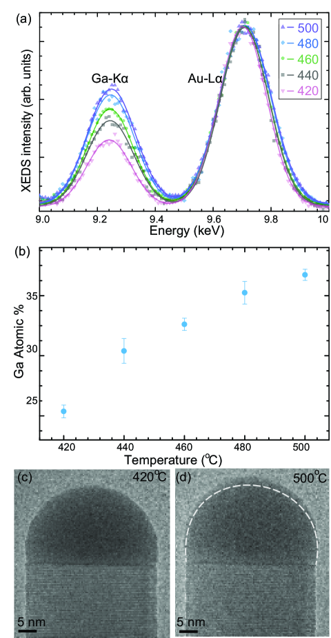
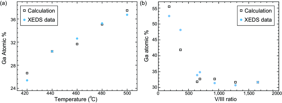
The composition of the catalyst particle during nanowire growth was measured as a function of temperature and is shown in Fig. 2 . During this experiment the Ga precursor flow was set to be relatively low (V/III = 1300; the relevance of this choice will be discussed later). More details of the experiment can be found in the Methods. The Ga content in the catalyst increases with temperature as can be observed in the XEDS spectra normalized to the Au-L peak (Fig. 2 (a)). Quantification of the XEDS spectra shows that when the temperature was increased monotonously from 440 ∘C to 500 ∘C the Ga content increased from 30 to 36 atomic % (Fig. 2 (b)). The temperature was then decreased to 420 ∘C, after which the Ga content decreased. A small but measurable change in the volume of the catalyst droplet at different temperatures was observed, as illustrated in Fig. 2 (c), indicating that the composition change is due primarily to an increase in Ga rather than a loss of Au atoms. (The correlation between Ga concentration and catalyst volume is discussed in more detail in Supplementary Information section S6)
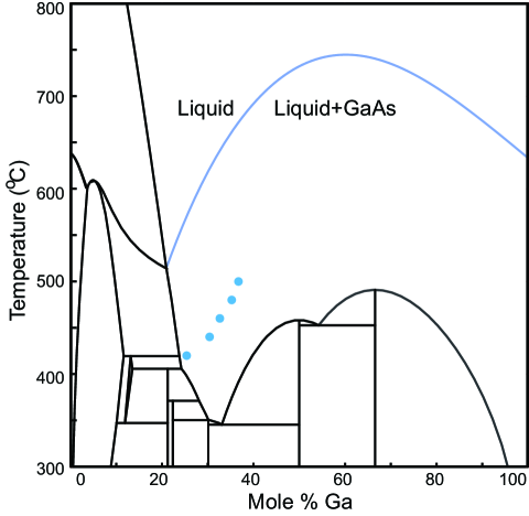
To understand the increase of Ga content in the catalyst with temperature we now consider some representative phase diagrams of the Au-Ga-As ternary alloy. Although nanowire growth is of course not an equilibrium process, phase diagrams can still be very useful in understanding the process by giving a visualization of the thermodynamic reference state of the system.[66] Fig. 3 (a) and (b) shows the ternary Au-Ga-As isothermal phase diagrams for two temperatures- 420 ∘C and 500 ∘C, calculated with the Thermo-Calc software using the thermodynamic data assessed by Ghasemi et al.[66] Note that the range of the plots shown here reaches 100 % for Ga and Au (x-axis), but only 0.2 % for As (y-axis). This range was chosen to clearly see the regions relevant for nanowire growth. Since for As 0.2 % there are no new phases formed compared to the ones already seen in Fig. 3 (a), (b), the phase diagram can be just extrapolated linearly for that regime. According to the phase diagram in Fig. 3 (a), a single phase stable liquid alloy of Au-Ga-As exists in a very narrow range of the ternary composition near As 0.01 %, Ga 26 % and Au 74 %. At 500 ∘C this region is broader. For the nanowire material to nucleate or precipitate out of the liquid catalyst alloy, the liquid catalyst alloy should first cross the liquidus line and reach a supersaturated/supercooled state.[66] Supersaturation in this scenario means that there would be more Ga and As in the catalyst than in a corresponding alloy at thermodynamic equilibrium. The maximum allowed As or Ga content, such that the alloy remains a liquid at equilibrium, is given by the liquidus line (blue line in Fig. 3). In other words, the liquidus separates the stable liquid alloy and a two-phase region with coexistence of solid GaAs and a Au-Ga-As ternary liquid. A supersaturated liquid alloy would hence be slightly above or on the right side of the blue liquidus line in Fig. 3 (keeping in mind that the number of excess atoms required to form an entire GaAs bilayer would correspond to about 1 % in the Au droplet for the catalyst/nanowire dimensions discussed here). So for a basic understanding of the process let us consider that the nanowire growth happens at (or more precisely, immediately beyond) the liquidus line.
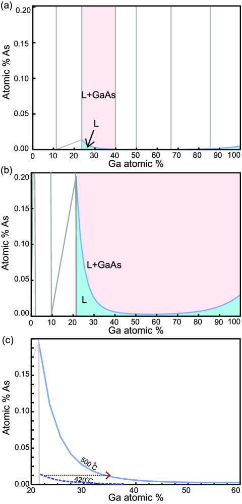
The liquidus shifts to higher Ga content at higher temperature (Fig. 3). Fig. 3 (c) shows a magnified section of Fig. 3 (b) (at 500 ∘C) where the liquidus at 420 ∘C is overlayed on it as a blue dashed curve. In principle, when the temperature is changed both the Ga and As concentrations in the catalyst could change. However, the As concentration in the catalyst would equilibrate with the ambient AsH3 partial pressure.[65] Since in this experiment the AsH3 flow is fixed, the As content in the catalyst would be mostly invariant with temperature.
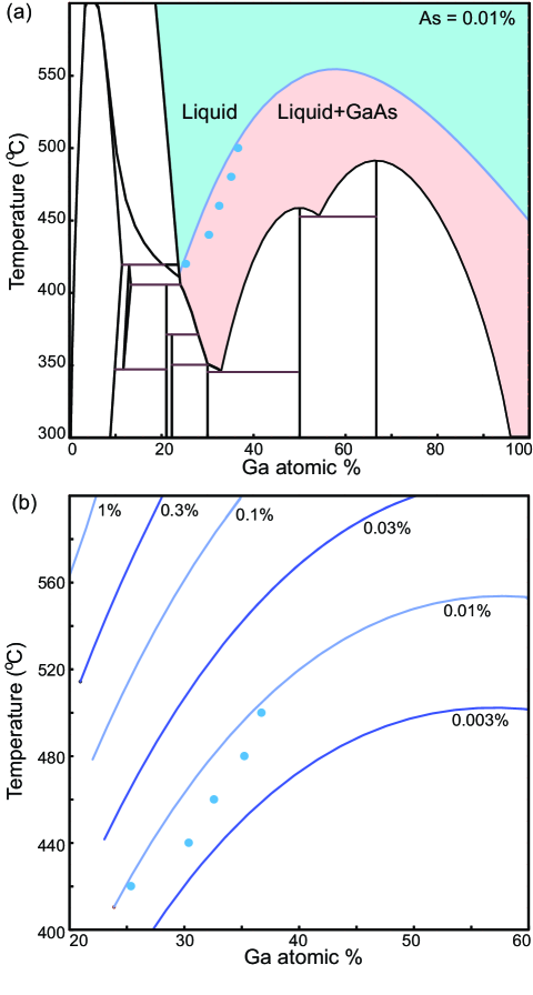
Let us now look at calculated phase diagrams at a few different As concentrations. We see that the Ga concentration measured experimentally by XEDS at different temperatures (blue dots in Fig. 4 (a)) is in close agreement with Ga concentration of the liquidus line calculated for As = 0.01 %. This close agreement in liquidus shape and experimental data indicates that the As content likely does not change very much with temperature, since this would result in a steeper temperature dependence of the liquidus (less change of Ga with temperature) according to Fig. 3 (c). The requirement of supersaturation implies that the measured composition should be such that Ga is more than the corresponding equilibrium concentration and hence on the right side of the liquidus line (blue). It is clear that As % cannot be much lower than 0.01 % while still fulfilling this condition: for instance As 0.003 % would imply that the Ga concentration is not sufficient to supersaturate the catalyst particle, as the measured Ga content would be less than the equilibrium Ga content (the liquidus line concentration) (Fig. 4 (b)).
On the other hand, for higher As, the liquidus line moves upwards in temperature, which limits how high the As content can be in a fully liquid catalyst at equilibrium. The Ga concentration varies during growth and is highest at nucleation and lowest after completion of a layer. When the Ga is at its lowest, it is likely that it reaches equilibrium. If this equilibrium does not correspond to a liquidus, there is a high chance that solid gold-containing phases form, and this we do not observe. An upper limit of the As concentration of 0.3 % can be estimated such that a liquidus exists at the investigated temperatures. The full phase diagram calculated for As of 0.3 % can be found in the Supplementary Information section S5. Note that in the experiment discussed, the temperature was varied from 440 ∘C to 500 ∘C by increasing the temperature in steps, so no super-cooling effects would appear in this range. Additionally, we must emphasize that since the XEDS spectra were collected for several minutes, the measured composition represents the average over time rather than the maximum supersaturation reached (which would correspond to the supersaturation at the nucleation of a new layer).
In short we estimate the average As concentration in this Au-Ga-As liquid alloy to be in the order of 0.01% (or in the range 0.01 %As0.3 %) in the temperature ranges typically used for GaAs nanowire growth in the high V/III regime. Although this value is low, it is consistent with theoretical estimates for such low AsH3 flows as used here.[65] Moreover, 0.01 % As in a droplet of this size corresponds to around 100 atoms, which is sufficient to form a critical nucleus to initiate a new GaAs bilayer. We note that this As content may also increase slightly with temperature, but the change should still fall within this overall range. This study also illustrates the value of phase diagrams to aid in the qualitative understanding of nanowire growth mechanisms.
Catalyst composition as a function of precursor flux
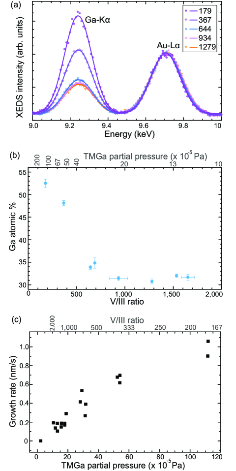
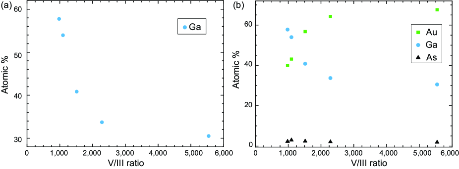
V/III ratio i.e. the ratio of the group V precursor flux (AsH3 here) to the group III precursor (TMGa here), is a very important parameter for the growth of III-V semiconductors. We now discuss the change of catalyst composition as a function of V/III ratio, at a fixed temperature of 420 ∘C measured on another nanowire (Fig. 5 (a), (b)). (Please see Methods section for details on how the V/III ratio is measured in this experiment.) We had set the AsH3 flow to be fixed and changed only the TMGa flow in this experiment. When the TMGa flow was stopped the nanowire was neither growing nor etching; the Ga content in the catalyst was measured to be 27 % by XEDS. (At elevated temperatures GaAs gets slowly etched by the Au-based catalyst if the precursors are not supplied appropriately.[4]) The Ga concentration in the catalyst then increases monotonically with increasing Ga precursor flux. At high V/III ratios (or low TMGa) a small increase of TMGa does not change the Ga concentration much; in fact, the Ga concentration is effectively constant within the resolution limit of the XEDS measurement. Since the Ga content is in a steady state (between incoming Ga, controlled by the TMGa flow, and outgoing Ga, primarily controlled by the nanowire growth), this result suggests that the nanowire growth is mainly limited by the TMGa flow in this regime. This is the regime that we used for studying the effect of temperature on the catalyst composition, and serves as further confirmation that a thermodynamic (rather than kinetic) understanding of the temperature trend is appropriate.
At low V/III ratios i.e. below about 900 (Fig. 5 (b)), the Ga concentration increases rapidly with increasing TMGa. (A similar increase of Ga content at lower V/III ratio was seen at 500 ∘C also as is shown in Supplementary Information section S4.) This trend in the measured composition by XEDS is accompanied by a large, clearly visible increase in the size of the catalyst droplet. Similar swelling of the catalyst at low V/III has previously been observed both ex situ[67, 68] and in situ[51, 52], and has also been predicted theoretically[69]. Previous reports have associated this effect with a transition to a ‘V-limited regime’ where the Ga supply is effectively higher than the As supply, and so excess Ga accumulates in the droplet before reaching a new quasi-steady-state composition.[51, 52] If we consider this in terms of the phase diagram in Fig. 3 (a), the results indicate that the As concentration of the droplet is constant when TMGa is low (equilibrating with the As in the vapor as predicted theoretically[65]). For high TMGa, the increased Ga in the droplet may suggest that the As concentration decreases with decreasing V/III ratio.
The average growth rate of the nanowire as a function of TMGa partial pressure (and V/III ratio) is shown in Fig. 5 (c). It is clear that the growth rate increases with TMGa flow over the full range. The trend is not linear however: for low TMGa (high V/III), there is a steep increase, but at higher TMGa (low V/III) this trend slows, potentially saturating at very high TMGa. The apparently linear trend between growth rate and TMGa for low TMGa flow is consistent with our interpretation above that the (effectively) constant Ga concentration in the catalyst is a consequence of Ga limiting the growth rate. Following the reasoning of Mårtensson et al.[65], we conclude that when AsH3 is very much in excess, the As concentration in the catalyst quickly reaches a maximum concentration which is in steady state with re-evaporation to the vapor; so long as the nucleation barrier does not shift significantly with growth parameters, the growth rate is limited by the time required for the Ga concentration to reach the level needed to overcome the nucleation barrier. The weakening of this trend at high TMGa, where increased Ga is observed in the catalyst, indicates a transition to a growth regime where As plays a limiting role. In this regime, the high TMGa flow allows the Ga concentration to exceed the value reached in the high V/III regime, before the As reaches the concentration that would be in steady state with vapor. Since the supersaturation is determined by both Ga and As species, the nucleation barrier is then reached for higher Ga and lower As concentrations (determined by the V/III ratio). The growth rate will then depend on both TMGa and AsH3 flows. True As-limited growth would be predicted for even higher TMGa flows, although it is not clear whether such a regime could actually be reached in experiments.
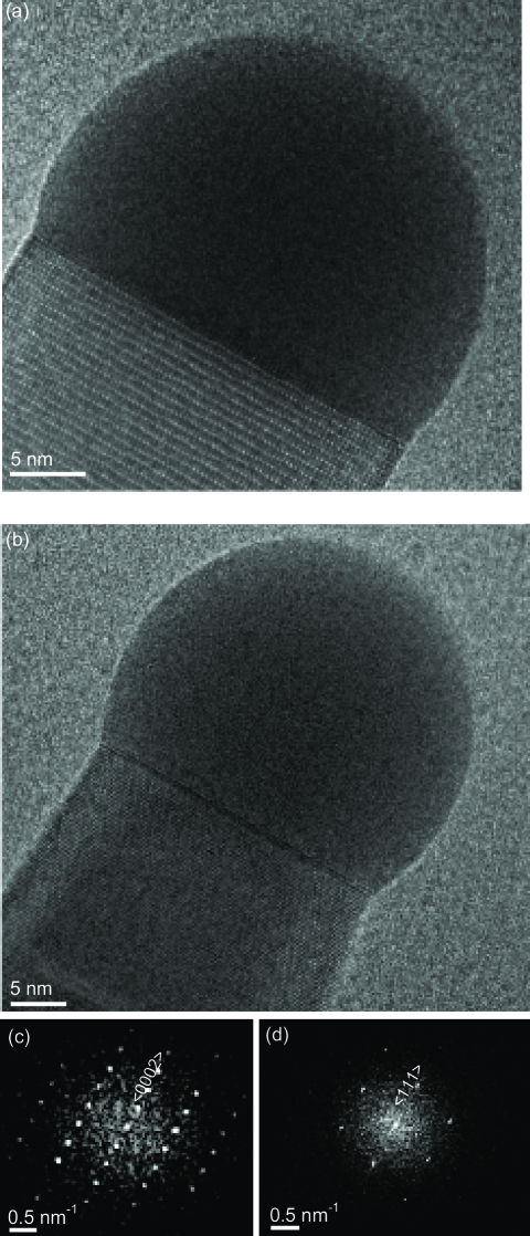
In addition to the change of the droplet size with V/III ratio, a change in the crystal structure of the nanowire was also observed. In the high V/III ratio regime (about 800-1700) the nanowire grew in the wurtzite structure along the 0001 direction (Fig. 6 (a), (c)). When the V/III ratio was decreased, stacking faults started to appear in the wurtzite nanowire. At even lower V/III ratios close to 350 the nanowire grew as a mixture of both zincblende and wurtzite structures. At still lower V/III ratio of about 180, the same nanowire grew in the zincblende structure along the 111 axis (Fig. 6 (b), (d)). The change of nanowire structure from zincblende to wurtzite with increasing V/III has been reported experimentally[67, 52] and theoretically[24]. MOCVD experiments also show a second transition back to zincblende at very high V/III ratio[67, 65] but this regime was not covered in the experiments described here. We have also observed in other experiments that, for even higher TMGa flows than studied here, the interface develops an oscillating truncation consistent with earlier in situ observations.[49, 50, 51, 52] Since the interface dynamics are qualitatively very different in that regime, it was not covered during the experiments that are included in this study.
Conclusions
In summary, GaAs nanowires were grown with a gold-based catalyst particle in an environmental TEM in order to deepen the understanding of nanowire growth. The chemical composition of the catalyst particle was measured in situ as the nanowire was growing. We report the catalyst composition during growth of one nanowire as a function of temperature and another wire of similar dimensions as a function of ratio of precursor flux. The Ga content in the catalyst increases with increasing temperature which correlates well with calculated phase diagrams. Since the concentration seems to be determined by thermodynamics, the results would be applicable to Au-catalyzed growth of GaAs nanowires independent of the growth method. Although the As content in the catalyst is below the detection limit by XEDS, by comparing measured Ga-Au content with calculated Au-Ga-As phase diagrams we can estimate the As concentration. The Ga concentration in the catalyst also increases with increasing Ga-precursor flux. These in situ measurements will aid better theoretical modelling of nanowire growth and improve the understanding of nanowire growth mechanisms. Most metal assisted III-V and II-VI nanowire growths typically have low solubility of the anion in the catalyst and the Au assisted GaAs studied here serves as a model system.
Methods
Au aerosol particles of 30 nm diameter on average were used to seed nanowire growth. A silicon nitride MEMS heating chip from Norcada was used as substrate. The thinnest SiNx parts where growth was monitored had a thickness of 30 nm. Atomic resolved imaging was performed with an AMT XR401 sCMOS camera and the videos were recorded at about 20 fps. The TEM images in the article were extracted from these videos and processed.
GaAs nanowires were grown in a Hitachi HF3300S environmental transmission electron microscope (ETEM) with CEOS B-COR-aberration-corrector and a cold field emission gun. Blaze software by Hitachi was used to control the local sample temperature using Joule heating in a constant power mode. The ETEM was connected to a gas handling system with the CVD gases. A single tilt holder that has two separate microtubes running to the holder tip was used for supplying gases. The holder and the gas handling system are connected by a polymer coated thin quartz tube (PEEKSil) from Trajan Scientific.
Pressure at the sample: During growth experiments the pressure near the pole piece was measured by an Inficon MPG400 pressure gauge and is referred to as ‘column pressure’ here. The precursor inlet tubes run along the length of the TEM holder, and precursor gases are released close to the heated SiNx grid. Hence the pressures are higher at the growth front than the ‘column pressure’. The sample pressure relative to the column pressure was calibrated using the pressure at the heating coil of a clean SiNx grid (without Au or GaAs) as a pressure gauge following the Pirani gauge principles using the Blaze software. We performed a calibration experiments with N2 and also H2 and found that the pressure at the sample (measured by Blaze) is twice of ‘column pressure’. A factor of 2 is therefore used to estimate sample pressure for each species based on its calibrated column pressure.
Precursor partial pressures and V/III ratio: The TMGa bubbler was maintained at -10 ∘C with H2 bubbled through it. Additionally, a small fixed amount of H2 dilution (to be more precise, four times the flow used for the bubbler) was added in the TMGa line followed the bubbler. No additional carrier gas was used, and the H2 partial pressure is thus much lower than in a typical MOCVD. The flow of the TMGa/H2 mixture was controlled by mass flow controller (MFC), and a portion of the resulting flow was bypassed to the vent line to restrict the pressure reaching the microscope.
In order to determine the partial pressure of TMGa at the sample, the precursor fluxes sent to the ETEM were monitored with a residual gas analyzer (SRS RGA 300) using mass spectrometry in these experiments. The amount of the dominant TMGa derivatives (containing Ga) are measured at mass-to-charge ratio of 101, 99, 71 and 69 associated with dimethylgallium and Ga. The sample heating is very local at the SiNx grid, decomposing just a very small fraction of the supplied precursors and so these RGA measurements are independent of localized pyrolysis at the sample. Calibration experiments were performed for different but known TMGa and H2 flows to find the correlation between ‘column pressure’ and the sum of the Ga-related mass spectrometry readings (‘column pressure’ in this case was corrected for H2 using Inficon MPG400 pressure gauge calibration factor). TMGa partial pressure at the sample during experiments is therefore determined using the calibrated RGA readings together with the factor of 2 between column pressure and sample pressure described above.
The AsH3 flow was controlled exclusively by MFC (no part bypassed) and fixed for all experiments to give an estimated pressure of 0.1 Pa ‘column pressure’, i.e. equivalently 0.2 Pa at the sample. Since the Inficon MPG400 pressure gauge is originally calibrated for N2, this AsH3 ‘column pressure’ was measured in comparison to an equivalent flow of N2 gas. V/III ratio is then calculated using this value divided by the TMGa pressure calculated using RGA readings for the specific experiment.
XEDS : The XEDS measurement was performed with a SDD X-MaxN 80 T system from Oxford Instruments. While measuring the catalyst composition a small condenser aperture was used and condensed the beam on the anterior part of the catalyst (opposite to the nanowire/catalyst interface). As the nanowire grows the catalyst particle keeps moving forward. During XEDS the illuminated area on the fluorescent screen was continuously monitored and the sample moved appropriately. We specify the percentage content of the elements in terms of atomic percentage (and not as weight percentage) throughout this paper. Data was acquired and quantified with Aztec software. Acquisition was typically for 4 minutes. In XEDS scans we observe signals of Au, Ga and As from the catalyst and/or nanowire, Si and N from the substrate and Cu due to scattering from parts of the microscope. The sum of Ga and Au signal is normalized to 100 atomic % to obtain results quoted in this article. The default lines (K for Ga, L for Au, K for As) were used for quantification. The standard deviation of quantification result is shown as the y-axis error in Fig. 2 (b) and Fig. 5 (b). More details about the XEDS quantification results are given in Supplementary Information section S3.
Arsenic content from XEDS: Typically, the measured As signal is very weak and a clear peak cannot necessarily be distinguished from background. Full quantification of spectra (including background and artefacts such as Si, N, etc) yields an As weight % of less than one, which is close to the detection limit in XEDS. Moreover, any small As signal detected may not necessarily originate from the catalyst nanoparticle. Since the nanowire is growing during the XEDS acquisition, the catalyst/nanowire interface moves; although spectra were acquired carefully to avoid the electron beam interacting with the nanowire directly, electrons scattered into the nanowire from the catalyst could easily lead to an overestimate of both Ga and As by a few percent.
Temperature series experiment: In the temperature series experiment discussed, temperature was increased from 440 ∘C to 500 ∘C in steps of 20 ∘C, and finally decreased to 420 ∘C. After each temperature was reached we waited at least a minute so that the catalyst stabilizes and there is no evident change in its dimensions. This wire grew in the wurtzite structure in the 0001 direction at the conditions studied.
V/III series experiment: The measurement for the V/III series were recorded at 420 ∘C. We started to observe the nanowire when the V/III was 1535 where we measured the first EDX data. Then the Ga supply was stopped for some time. The TMGa flow was restarted and increased slowly in steps until (at very high flow) the nanowire changed direction and folded back on itself during an XEDS acquisition. During the XEDS measurement at the lowest V/III ratio (179) there was some As signal observed due to scattering from GaAs NW, so the same percentage of Ga was subtracted from the quantification results and renormalized to obtain the data point plotted. (See Supplementary data section S3 for details)The range about which V/III varied during individual XEDS spectrum acquisition is denoted by the error bar for the x-axis in Fig. 5 (b).
Data Availability
More data that support the findings of this study are available from the corresponding author upon request.
References
References
- [1] Y. N. Guo, J. Zou, M. Paladugu, H. Wang, Q. Gao, H. H. Tan, and C. Jagadish. Structural characteristics of GaSb/GaAs nanowire heterostructures grown by metal-organic chemical vapor deposition. Applied physics letters, 89(23):231917, 2006.
- [2] M. W. Larsson, J. B. Wagner, M. Wallin, P. Håkansson, L. E. Fröberg, L. Samuelson, and L. R. Wallenberg. Strain mapping in free-standing heterostructured wurtzite InAs/InP nanowires. Nanotechnology, 18(1):015504, 2006.
- [3] P. Caroff, M. E. Messing, B. M. Borg, K. A. Dick, K. Deppert, and L. E. Wernersson. InSb heterostructure nanowires: MOVPE growth under extreme lattice mismatch. Nanotechnology, 20(49):495606, 2009.
- [4] A. I. Persson, M. W. Larsson, S. Stenström, B. J. Ohlsson, L. Samuelson, and L. R. Wallenberg. Solid-phase diffusion mechanism for GaAs nanowire growth. Nature Materials, 3(10):677–681, October 2004.
- [5] B. W. Jacobs, V. M. Ayres, M. P. Petkov, J. B. Halpern, M. He, A. D. Baczewski, K. McElroy, M. A. Crimp, J. Zhang, and H. C. Shaw. Electronic and structural characteristics of zinc-blende wurtzite biphasic homostructure GaN nanowires. Nano letters, 7(5):1435–1438, 2007.
- [6] H. J. Joyce, J. Wong-Leung, Q. Gao, H. H. Tan, and C. Jagadish. Phase perfection in zinc blende and wurtzite III-V nanowires using basic growth parameters. Nano Letters, 10(3):908–915, March 2010.
- [7] K. A. Dick, P. Caroff, J. Bolinsson, M. E. Messing, J. Johansson, K. Deppert, L. R. Wallenberg, and L. Samuelson. Control of III-V nanowire crystal structure by growth parameter tuning. Semiconductor Science and Technology, 25(2):024009, 2010.
- [8] S. Sukrittanon, Y. J. Kuang, A. Dobrovolsky, W. M. Kang, J. S. Jang, B. J. Kim, W. M. Chen, I. A. Buyanova, and C. W. Tu. Growth and characterization of dilute nitride GaNxP1-x nanowires and GaNxP1-x/GaNyP1-y core/shell nanowires on Si (111) by gas source molecular beam epitaxy. Applied Physics Letters, 105(7):072107, 2014.
- [9] L. Namazi, S. G. Ghalamestani, S. Lehmann, R. R. Zamani, and K. A. Dick. Direct nucleation, morphology and compositional tuning of InAs1-xSbx nanowires on InAs (111) B substrates. Nanotechnology, 28(16):165601, 2017.
- [10] V. G. Dubrovskii. Refinement of nucleation theory for vapor–liquid–solid nanowires. Crystal Growth & Design, 17(5):2589–2593, May 2017.
- [11] K. W. Schwarz and J. Tersoff. Elementary processes in nanowire growth. Nano Letters, 11(2):316–320, February 2011.
- [12] V. A. Nebolflsin and A. A. Shchetinin. Role of surface energy in the vapor–liquid–solid growth of silicon. Inorganic Materials, 39(9):899–903, September 2003.
- [13] P. Krogstrup, H. I. Jørgensen, E. Johnson, M. H. Madsen, Claus B. Sørensen, A. F. Morral, M. Aagesen, J. Nygård, and F. Glas. Advances in the theory of III-V nanowire growth dynamics. Journal of Physics D: Applied Physics, 46(31):313001, 2013.
- [14] F. Glas. Chemical potentials for Au-assisted vapor-liquid-solid growth of III-V nanowires. Journal of Applied Physics, 108(7):073506, October 2010.
- [15] V. G. Dubrovskii. Group V sensitive vapor–liquid–solid growth of Au–catalyzed and self–catalyzed III-V nanowires. Journal of Crystal Growth, 440:62–68, April 2016.
- [16] M. C. Plante and R. R. LaPierre. Analytical description of the metal-assisted growth of III-V nanowires: Axial and radial growths. Journal of Applied Physics, 105(11):114304, June 2009.
- [17] M. R. Ramdani, J. C. Harmand, F. Glas, G. Patriarche, and L. Travers. Arsenic pathways in self-catalyzed growth of GaAs nanowires. Crystal Growth & Design, 13(1):91–96, January 2013.
- [18] V. G. Dubrovskii, N. V. Sibirev, R. A. Suris, G. E. Cirlin, J. C. Harmand, and V. M. Ustinov. Diffusion–controlled growth of semiconductor nanowires: Vapor pressure versus high vacuum deposition. Surface Science, 601(18):4395–4401, September 2007.
- [19] F. Glas, J. C. Harmand, and G. Patriarche. Why does wurtzite form in nanowires of III-V zinc blende semiconductors? Physical Review Letters, 99(14):146101, October 2007.
- [20] V. G. Dubrovskii, N. V. Sibirev, J. C. Harmand, and F. Glas. Growth kinetics and crystal structure of semiconductor nanowires. Physical Review B, 78(23):235301, December 2008.
- [21] J. Johansson, Z. Zanolli, and K. A. Dick. Polytype attainability in III-V semiconductor nanowires. Crystal growth & design, 16(1):371–379, 2015.
- [22] M. Tornberg, K. A. Dick, and S. Lehmann. Thermodynamic stability of gold-assisted InAs nanowire growth. The Journal of Physical Chemistry C, 121(39):21678–21684, 2017.
- [23] F. Panciera, M. M. Norton, S. B. Alam, S. Hofmann, K. Mølhave, and F. M. Ross. Controlling nanowire growth through electric field-induced deformation of the catalyst droplet. Nature Communications, 7:12271, July 2016.
- [24] V. G. Dubrovskii. Mono- and polynucleation, atomistic growth, and crystal phase of III-V nanowires under varying group V flow. The Journal of Chemical Physics, 142(20):204702, May 2015.
- [25] P. Krogstrup, S. Curiotto, E. Johnson, M. Aagesen, J. Nygård, and D. Chatain. Impact of the liquid phase shape on the structure of III-V nanowires. Physical Review Letters, 106(12):125505, March 2011.
- [26] R. E. Algra, V. Vonk, D. Wermeille, W. J. Szweryn, M. A. Verheijen, W. J. P. van Enckevort, A. A. C. Bode, W. L. Noorduin, E. Tancini, A. E. F. de Jong, E. P. A. M. Bakkers, and E. Vlieg. Formation of wurtzite InP nanowires explained by liquid-ordering. Nano Letters, 11(1):44–48, January 2011.
- [27] V. G. Dubrovskii and N. V. Sibirev. General form of the dependences of nanowire growth rate on the nanowire radius. Journal of crystal growth, 304(2):504–513, 2007.
- [28] L. E. Fröberg, W. Seifert, and J. Johansson. Diameter-dependent growth rate of InAs nanowires. Physical Review B, 76(15):153401, 2007.
- [29] N. Li, W. Li, L. Liu, and T. Y. Tan. A nucleation-growth model of nanowires produced by the vapor-liquid-solid process. Journal of Applied Physics, 114(6):064302, 2013.
- [30] M. T. Borgström, G. Immink, B. Ketelaars, R. Algra, and E. P. A. M. Bakkers. Synergetic nanowire growth. Nature nanotechnology, 2(9):541, 2007.
- [31] A. Li, N. V. Sibirev, D. Ercolani, V. G Dubrovskii, and L. Sorba. Readsorption assisted growth of InAs/InSb heterostructured nanowire arrays. Crystal Growth & Design, 13(2):878–882, 2013.
- [32] B. M. Borg, J. Johansson, K. Storm, and K. Deppert. Geometric model for metalorganic vapour phase epitaxy of dense nanowire arrays. Journal of Crystal Growth, 366:15–19, 2013.
- [33] M. Ek and M. A. Filler. Atomic–scale choreography of vapor–liquid–solid nanowire growth. Accounts of Chemical Research, 51(1):118–126, January 2018.
- [34] M. Kirkham, Z. L. Wang, and R. L. Snyder. Tracking the catalyzed growth process of nanowires by in situ x-ray diffraction. Journal of Applied Physics, 108(1):014304, 2010.
- [35] P. Schroth, M. Köhl, J. W. Hornung, E. Dimakis, C. Somaschini, L. Geelhaar, A. Biermanns, S. Bauer, S. Lazarev, U. Pietsch, et al. Evolution of polytypism in GaAs nanowires during growth revealed by time-resolved in situ x-ray diffraction. Physical review letters, 114(5):055504, 2015.
- [36] P. Krogstrup, M. Hannibal Madsen, W. Hu, M. Kozu, Y. Nakata, J. Nygård, M. Takahasi, and R. Feidenhansfll. In-situ x-ray characterization of wurtzite formation in GaAs nanowires. Applied Physics Letters, 100(9):093103, 2012.
- [37] S. V. Sivaram, H. Y. Hui, M. de la Mata, J. Arbiol, and M. A. Filler. Surface hydrogen enables subeutectic vapor–liquid–solid semiconductor nanowire growth. Nano Letters, 16(11):6717–6723, November 2016.
- [38] S. V. Sivaram, N. Shin, L. W. Chou, and M. A. Filler. Direct observation of transient surface species during Ge nanowire growth and their influence on growth stability. Journal of the American Chemical Society, 137(31):9861–9869, 2015.
- [39] N. Shin, M. Chi, and M. A. Filler. Interplay between defect propagation and surface hydrogen in silicon nanowire kinking superstructures. ACS nano, 8(4):3829–3835, 2014.
- [40] M. Tchernycheva, J. C. Harmand, G. Patriarche, L. Travers, and G. E. Cirlin. Temperature conditions for GaAs nanowire formation by Au-assisted molecular beam epitaxy. Nanotechnology, 17(16):4025, 2006.
- [41] T. Xu, K. A. Dick, S. Plissard, T. H. Nguyen, Y. Makoudi, M. Berthe, J. P. Nys, X. Wallart, B. Grandidier, and P. Caroff. Faceting, composition and crystal phase evolution in III-V antimonide nanowire heterostructures revealed by combining microscopy techniques. Nanotechnology, 23(9):095702, 2012.
- [42] J. Jo, Y. Tchoe, G. C. Yi, and M. Kim. Real-time characterization using in situ RHEED transmission mode and TEM for investigation of the growth behaviour of nanomaterials. Scientific reports, 8(1):1694, 2018.
- [43] M. Heurlin, N. Anttu, C. Camus, L. Samuelson, and M. T. Borgström. In situ characterization of nanowire dimensions and growth dynamics by optical reflectance. Nano letters, 15(5):3597–3602, 2015.
- [44] T. Clement, S. Ingole, S. Ketharanathan, J. Drucker, and S. T. Picraux. In situ studies of semiconductor nanowire growth using optical reflectometry. Applied physics letters, 89(16):163125, 2006.
- [45] S. Fernández-Garrido, J. K. Zettler, L. Geelhaar, and O. Brandt. Monitoring the formation of nanowires by line-of-sight quadrupole mass spectrometry: a comprehensive description of the temporal evolution of gan nanowire ensembles. Nano letters, 15(3):1930–1937, 2015.
- [46] M. Kolíbal, T. Pejchal, T. Vystavel, and T. Sikola. The synergic effect of atomic hydrogen adsorption and catalyst spreading on Ge nanowire growth orientation and kinking. Nano letters, 16(8):4880–4886, 2016.
- [47] S. Kodambaka, J. Tersoff, M. C. Reuter, and F. M. Ross. Germanium nanowire growth below the eutectic temperature. Science, 316(5825):729–732, May 2007.
- [48] S. Hofmann, R. Sharma, C. T. Wirth, F. Cervantes-Sodi, C. Ducati, T. Kasama, R. E. Dunin-Borkowski, J. Drucker, P. Bennett, and J. Robertson. Ledge-flow-controlled catalyst interface dynamics during Si nanowire growth. Nature Materials, 7(5):372, May 2008.
- [49] C.-Y. Wen, J. Tersoff, K. Hillerich, M. C. Reuter, J. H. Park, S. Kodambaka, E. A. Stach, and F. M. Ross. Periodically changing morphology of the growth interface in Si, Ge, and GaP nanowires. Physical Review Letters, 107(2):025503, July 2011.
- [50] A. D. Gamalski, C. Ducati, and S. Hofmann. Cyclic supersaturation and triple phase boundary dynamics in germanium nanowire growth. The Journal of Physical Chemistry C, 115(11):4413–4417, 2011.
- [51] Y.-C. Chou, K. Hillerich, J. Tersoff, M. C. Reuter, K. A. Dick, and F. M. Ross. Atomic-scale variability and control of III-V nanowire growth kinetics. Science, 343(6168):281–284, January 2014.
- [52] D. Jacobsson, F. Panciera, J. Tersoff, M. C. Reuter, S. Lehmann, S. Hofmann, K. A. Dick, and F. M. Ross. Interface dynamics and crystal phase switching in GaAs nanowires. Nature, 531(7594):317, March 2016.
- [53] J. C. Harmand, G. Patriarche, F. Glas, F. Panciera, I. Florea, J. L. Maurice, L. Travers, and Y. Ollivier. Atomic step flow on a nanofacet. Physical Review Letters, 121(16):166101, October 2018.
- [54] A. D. Gamalski, J. Tersoff, and E. A. Stach. Atomic resolution in situ imaging of a double-bilayer multistep growth mode in gallium nitride nanowires. Nano Letters, 16(4):2283–2288, April 2016.
- [55] V. G. Dubrovskii, Z. V. Sokolova, M. V. Rylkova, and A. A. Zhiglinsky. Composition and contact angle of Au-III-V droplets on top of Au-catalyzed III-V nanowires. Materials Physics and Mechanics, 36(1):1–7, 2018.
- [56] V. G. Dubrovskii and J. Grecenkov. Zeldovich nucleation rate, self-consistency renormalization, and crystal phase of Au-catalyzed GaAs nanowires. Crystal Growth & Design, 15(1):340–347, January 2015.
- [57] V. G. Dubrovskii. Influence of the group V element on the chemical potential and crystal structure of Au-catalyzed III-V nanowires. Applied Physics Letters, 104(5):053110, February 2014.
- [58] E. D. Leshchenko, M. Ghasemi, V. G. Dubrovskii, and J. Johansson. Nucleation-limited composition of ternary III-V nanowires forming from quaternary gold based liquid alloys. CrystEngComm, 20(12):1649–1655, 2018.
- [59] J. C. Harmand, G. Patriarche, N. Péré-Laperne, M. N. Mérat-Combes, L. Travers, and F. Glas. Analysis of vapor-liquid-solid mechanism in Au-assisted GaAs nanowire growth. Applied Physics Letters, 87(20):203101, November 2005.
- [60] D. Jacobsson, S. Lehmann, and K. A. Dick. Zincblende-to-wurtzite interface improvement by group III loading in Au-seeded GaAs nanowires. physica status solidi (RRL) – Rapid Research Letters, 7(10):855–859, October 2013.
- [61] C. Chatillon, F. Hodaj, and A. Pisch. Thermodynamics of GaAs nanowire MBE growth with gold droplets. Journal of Crystal Growth, 311(14):3598–3608, July 2009.
- [62] J. Tersoff. Stable self-catalyzed growth of III-V nanowires. Nano Letters, 15(10):6609–6613, October 2015.
- [63] L. H. G. Tizei, T. Chiaramonte, D. Ugarte, and M. A. Cotta. III-V semiconductor nanowire growth: does arsenic diffuse through the metal nanoparticle catalyst. Nanotechnology, 20(27):275604, 2009.
- [64] F. Glas, M. R. Ramdani, G. Patriarche, and J. C. Harmand. Predictive modeling of self-catalyzed III-V nanowire growth. Physical Review B, 88(19):195304, 2013.
- [65] E. K. Mårtensson, S. Lehmann, K. A. Dick, and J. Johansson. Simulation of GaAs nanowire growth and crystal structure. Nano letters, 2019.
- [66] M. Ghasemi and J. Johansson. Phase diagrams for understanding gold-seeded growth of GaAs and InAs nanowires. Journal of Physics D: Applied Physics, 50(13):134002, 2017.
- [67] S. Lehmann, D. Jacobsson, and K. A. Dick. Crystal phase control in GaAs nanowires: opposing trends in the Ga-and As-limited growth regimes. Nanotechnology, 26(30):301001, 2015.
- [68] D. L. Dheeraj, A. M. Munshi, M. Scheffler, A.T. J. van Helvoort, H. Weman, and B. O. Fimland. Controlling crystal phases in GaAs nanowires grown by Au-assisted molecular beam epitaxy. Nanotechnology, 24(1):015601, 2012.
- [69] V. G. Dubrovskii, Z. V. Sokolova, M. V. Rylkova, and A. A. Zhiglinsky. Composition and contact angle of Au-III-V droplets on top of Au-C III-V nanowires. Materials Physics and Mechanics, 36:1–7, 2018.
- [70] J. B. Hannon, S. Kodambaka, F. M. Ross, and R. M. Tromp. The influence of the surface migration of gold on the growth of silicon nanowires. Nature, 440(7080):69, 2006.
- [71] G. Otnes, M. Heurlin, M. Graczyk, J. Wallentin, D. Jacobsson, A. Berg, I. Maximov, and M. T. Borgström. Strategies to obtain pattern fidelity in nanowire growth from large-area surfaces patterned using nanoimprint lithography. Nano Research, 9(10):2852–2861, 2016.
Acknowledgments
We wish to acknowledge support from the Knut and Alice Wallenberg Foundation, NanoLund and the Swedish Research Council. We thank E. Mårtensson for valuable discussions and insights. We thank Joacim Gustafsson, Stas Dogel and Charles Soong from Hitachi and John Wheeler and Shaun Ohman from Collabratech for technical assistance in setting up the laboratory.
Author contributions
CBM, DJ, MT and ARP performed the experiments. Data analysis was done by CBM. JJ performed the phase diagram calculations. KAD and RW coordinated the project. All authors discussed the results and contributed to the concepts discussed in this article.
Competing financial interests
The authors declare no competing financial interests.
Supplementary Information: In situ analysis of catalyst composition during gold catalyzed GaAs nanowire growth
S1 Examples of catalyst composition measured ex situ from Au-assisted GaAs nanowire
The catalyst composition measured post-growth depends on the conditions used to terminate the growth. Some representative examples are shown in Table S1.
| Reference | Growth Technique | Cooling / growth termination | Ga% |
|---|---|---|---|
| Cooling in H2 environment of zincblende nanowires (grown with relatively less Ga precursor flux) | 21 | ||
| Jacobsson et al.[60] | MOCVD | Cooling in AsH3/H2 environment of zincblende nanowires (grown with relatively less Ga precursor flux) | 3 |
| Cooling in H2 environment of wurtzite nanowires (grown with relatively larger Ga precursor flux) | 31 | ||
| Cooling in AsH3/H2 environment of wurtzite nanowires (grown with relatively larger Ga precursor flux) | 3 | ||
| Ga stopped before As2 after growth | 1 | ||
| Harmand et al.[59] | Molecular Beam | Ga and As2 stopped simultaneously after growth | 50 |
| Epitaxy | Longer growth time to get tapered nanowires, then Ga and As2 stopped simultaneously | 31 | |
| Persson et al.[4] | Chemical Beam | Ga and As precursors stopped simultaneously after growth | 9 |
| Epitaxy | Cooled down in As | 0 |
S2 Statistics: XEDS from different nanowires at same conditions
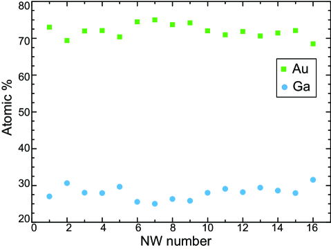
It is important to know that the catalyst composition across different particles is roughly the same at identical conditions. Hence we conducted experiment at 420 ∘C with a fixed low TMGa flow and measured the Ga concentration across different nanowire catalysts. They had roughly the same concentration. We also looked at diameter dependence of catalyst composition and found little difference in the range we measured (16 nm to 66 nm diameter during growth) (For this experiment we used Au nanoparticles with different sizes unlike the two sets of experiments reported in the article.)
S3 XEDS data measured for the temperature series and the V/III series
In the article (Fig. 2 (b) and 5 (b)) only the Ga concentration in the Au-Ga-As catalyst alloy was plotted. The XEDS quantification data measured including the background signal from the SiNx film is shown in the tables below. Table S2 is of the temperature series shown in Fig. 2 (b). Table S3 is of the V/III series shown in Fig. 5 (b). We suspect the As% observed arises mainly due to scattering from the adjacent GaAs nanowire. (Quantification of low energy peaks 0.5 keV are not available at 480 and 500 ∘C due to drastically increased strobe peak.)
| T(∘C) | Ga | As | Au | N | Si | Cu |
|---|---|---|---|---|---|---|
| 440 | 3.5 | 0.2 | 8.0 | 45.1 | 40.3 | 2.9 |
| 460 | 5.5 | 0.4 | 11.4 | 25.8 | 52.7 | 4.2 |
| 480 | 9.2 | 0.7 | 16.8 | - | 67.3 | 6.0 |
| 500 | 9.6 | 0.8 | 16.5 | - | 67.4 | 5.9 |
| 420 | 4.6 | 0.6 | 13.5 | 38.8 | 38.0 | 4.4 |
| V/III | Ga | As | Au | N | Si | Cu |
|---|---|---|---|---|---|---|
| 1535 | 4.6 | 0.3 | 9.7 | 45.1 | 38.0 | 2.5 |
| 11264 | 2.5 | 0.4 | 6.3 | 50.5 | 37.9 | 2.3 |
| 1651 | 3.0 | 0.2 | 6.4 | 56.7 | 31.4 | 2.2 |
| 1279 | 3.6 | 0.3 | 8.1 | 52.9 | 32.3 | 2.7 |
| 934 | 4.1 | 0.3 | 8.9 | 47.5 | 36.2 | 3.0 |
| 644 | 6.2 | 0.5 | 12.1 | 32.6 | 44.4 | 4.2 |
| 689 | 6.6 | 0.6 | 12.4 | 30.2 | 45.7 | 4.4 |
| 367 | 12.2 | 0.9 | 13.1 | 16.3 | 52.8 | 4.6 |
| 179 | 12.0 | 2.8 | 8.3 | 27.8 | 45.6 | 3.6 |
At the end of the V/III series experiment, during the XEDS at V/III=179, the nanowire changed direction and folded back onto itself. This gave rise to the relatively high As% observed at V/III=179 (Ga=52 %, Au=36 % and As=12 % with normalization Au+Ga+As=100%) Assuming that 12 % As and hence 12 % Ga came from scattering from the GaAs nanowire, and renormalizing gives Ga=52.5 %, Au=47.5 % which is plotted in Fig. 5 (b). At the beginning of this particular XEDS scan the catalyst composition measured was Ga=51 %, Au=45 % and As=4 % (with Au+Ga+As=100 %). In similar experiments conducted there was no additional As at low V/III, and Ga% always increased at low V/III ratio. An example of another V/III series experiment is shown in the next section.
S4 XEDS at 500 ∘C
The catalyst composition at 500 ∘C as a function of the V/III ratio is shown below (Fig. S2). As expected we see an increase in Ga with decreasing V/III ratio (or increasing TMGa flow.) The As content remains negligible all throughout. (This experiment was performed in the constant resistance mode of Blaze and the XEDS spectra were acquired for 2 minutes each.)
S5 Phase diagram with As = 0.3 %
Phase diagram section calculated for a fixed As concentration of 0.3 % overlaid with Ga% measured during the temperature series (Same experimental data as plotted in Fig. 2 (b) of the article).
S6 Ga from XEDS and volume change
As mentioned earlier, the volume of the catalyst particle can give an indirect estimate of the catalyst composition. This is a simple way, particularly useful if the TEM does not have any associated system for quantitative compositional analysis. However, this method assumes that Au is not diffusing out of the catalyst particle, which need not be true at all conditions. In cases where Au diffuses out of the catalyst, this indirect measurement becomes inaccurate. Very evident Au diffusion along Si nanowires during in situ experiments have been reported.[70] We have not noticed any obvious migration of Au in our videos, but it is in principle possible at high temperatures.[71] In some experiments (not discussed in this article) we observed tiny portions of the catalyst left on the sidewalls of the nanowire, which we do not know if it was pure Au or pure Ga or a Au-Ga mixture. Since the As concentration is very small, it’s contribution to the volume can be neglected. By correlating the volume change to the catalyst composition measured by XEDS, one can assess Au diffusion on GaAs nanowires at typical growth conditions.
The Ga concentration in the catalyst calculated from the volume for the temperature series experiment discussed earlier is plotted in Fig. S4 (a) as open black squares. For this calculation we have imposed that the volume measured at 440 ∘C is due to 30 % Ga, which is the XEDS value measured at 440 ∘C. The volume was calculated by treating the catalyst particle as a spherical cap and assuming the base of the catalyst to be a circle. The measured and calculated Ga% matches, indicating that the Au diffusion is negligible. (From the catalyst volume and Ga content measured during growth, the diameter of the starting Au seed particle can be calculated to be about 28 nm, assuming the starting Au seed would have been spherical. The exact dimensions of the catalyst giving this specific nanowire that was measured is unknown to us. But the average size of the Au particles deposited on the substrate during this experiment was about 30 nm in diameter, which agrees to the 28 nm we calculated for this particular nanowire.) Similarly, Ga% calculated from the volume for the V/III series is plotted in Fig. 5 (b). The normalization was done by setting the volume measured at V/III = 1651 to be due to the measured value of 31 % Ga. The catalyst shape was fitted with a prolate spheroid with the nanowire-catalyst interface being a circle.