Nanoelectromechanical resonators from high-Tc superconducting crystals of Bi2Sr2Ca1Cu2O8+δ
Abstract
In this report, we present nanoelectromechanical resonators fabricated with thin exfoliated crystals of a high-Tc cuprate superconductor Bi2Sr2Ca1Cu2O8+δ. The mechanical readout is performed by capacitively coupling their motion to a coplanar waveguide microwave cavity fabricated with a superconducting alloy of molybdenum-rhenium. We demonstrate mechanical frequency tunability with external dc-bias voltage, and quality factors up to 36600. Our spectroscopic and time-domain measurements show that mechanical dissipation in these systems is limited by the contact resistance arising from resistive outer layers. The temperature dependence of dissipation indicates the presence of tunneling states, further suggesting that their intrinsic performance could be as good as other two-dimensional atomic crystals such as graphene.
1 Introduction
Two-dimensional (2D) atomic crystals host a unique set of electrical, mechanical, and optical properties, which are significantly different than their bulk counterparts, and are important for their applications towards devices [1, 2, 3]. Understanding properties of 2D materials like graphene, NbSe2, MoS2, and black phosphorous has provided insight into the mechanical response [4, 5, 6, 7, 8, 9]. These insights include ultra-high mechanical strength, complex nonlinearities, anisotropic elastic properties, and coupling with correlated ground state like charge density wave [4, 10, 11, 7, 9]. From the family of 2D materials, atomically thin crystals of high-transition temperature (Tc) superconductor Bi2Sr2Ca1Cu2O8+δ (BSCCO) were exfoliated in the seminal work by Novoselov et al. [12], and have been studied to probe their phase diagram in few unit cell thick crystals [13, 14, 15].
High-Tc superconductors host a rich variety of phases, which are important for the understanding of the microscopic mechanism of superconductivity in these materials [16]. Exfoliable thin superconducting crystals provide an avenue to study different quantum phase with in-situ tuning of carrier density, revealing nature of the two-dimensional superconductivity [17, 18]. Naturally, exploring the elastic properties of high-Tc superconductors with temperature, in the few unit cell limit is interesting for fundamental and applied aspects.
Apart from their rich electronic properties, thin superconducting crystals are attractive for developing cavity-optomechanical systems [19]. Their low mass and hence large quantum zero-point fluctuations make them attractive for achieving large coupling strength to electromagnetic fields. Recently, there has been an intense interest in exploring materials like graphene, NbSe2 etc. to develop optomechanical devices [20, 21], where high conductivity nature of these materials tends to minimize the resistive dissipation for microwave signal [22]. Moreover, a sensitive detection of elastic properties by cavity optomechanics could be an interesting technique for investigating phase-transition in these materials, providing additional insights which may not be captured by the conventional measurements of thermodynamic quantities [23, 24].
Here, we take the first step in this direction by probing an optomechanical system consisting of multilayer BSCCO membrane coupled to a microwave cavity. Our device-design enables addition of a dc bias voltage, which is used to tune the resonant frequency of mechanical resonator. We measure dissipation at ultra-low temperatures in these resonators using spectroscopic and time-domain techniques. Based on capacitive-circuit damping model, we quantify the dc-bias dependence of dissipation. These observations suggest that the quality factor of BSCCO is primarily limited by the contact resistance arising from the resistive outer layers.
2 Device fabrication
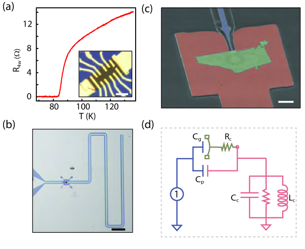
The BSCCO crystals in the form of whiskers were grown using a previously reported technique [25]. Due to the sensitivity of BSCCO to the ambient conditions, the grown whiskers were stored at liquid nitrogen temperature to keep them away from moisture, and to suppress the mobility of interstitial oxygen dopants. These whiskers were taken out from liquid nitrogen only at the time of exfoliation. Fig. 1(a) shows the measurement of 4-probe resistance with temperature for a flake of 40 nm thickness, revealing a superconducting transition temperature of 83 K. All the devices discussed here were fabricated by mechanical exfoliation from whiskers grown in this run.
To perform readout of the nanomechanical resonators of BSCCO at low temperatures, we capacitively couple their motion to a microwave cavity. Here a thin exfoliated flake from BSCCO crystals is used to form a coupling capacitor to a quarter wavelength coplanar waveguide resonator having 50 impedance and fabricated with an alloy of molybdenum and rhenium (Mo-Re) which has a superconducting transition temperature 11 K. Alloys of Mo-Re have been reported to show high-quality factor and low contact resistance in a wide variety of systems [20, 26, 27, 28]. The surface of Mo-Re offers a better adhesion with exfoliated flakes compared to other commonly used superconductors such as aluminum which are prone to surface oxidation.
To fabricate the microwave cavity, an intrinsic silicon wafer was first extensively cleaned using nitric acid, followed by a 5 min long dip in hydrofluoric acid, and finally a rinse in running DI water. A cleaned silicon wafer was then immediately loaded into the sputter chamber to minimize the oxidation of pristine Si-substrate. A 300 nm thick film of Mo-Re is then deposited using DC-magnetron sputtering. To pattern the Mo-Re film, we prepare a trilayer etch mask, consisting of : 50 of diluted-LOR in cyclo-pentanone, 15 nm Al-layer, and 250 nm of PMMA 950 A4 e-beam resist. The top e-beam resist is patterned by lithography. Chlorine plasma is then used to etch the thin Al layer, and subsequently O2 plasma is used to etch the underneath LOR layer. To etch Mo-Re, we have used SF6 plasma. Due to the immunity of Al layer to the SF6 plasma, it acts as a good mask for the patterning of Mo-Re. The etch mask is finally stripped-off using a photo-developer and N-Methyl-2-pyrrolidone. With an additional step of lithography and etching, the Mo-Re film is thinned down near the coupling to the external feedline, and thus forms a part of the capacitive coupler. Fig. 1(b) shows an optical microscope image of a fabricated quarter-wavelength cavity with Mo-Re on an intrinsic silicon substrate. It is worth to point out here that using the resist stack and lithography steps mentioned above, we consistently measure internal dissipation rates of microwave resonators to be less than 100 kHz on intrinsic Si substrate.
BSCCO flakes are then exfoliated in the ambient environment and transferred to the cavity using a deterministic dry-transfer technique [29]. Fig. 1(c) shows a zoomed in SEM image of a BSCCO flake in the shape of a drumhead mechanical resonator, forming a coupling capacitor to the cavity. It has a thickness of 54 nm and is suspended by 178 nm over the bottom plate, partially visible through the flake. Fig. 1(d) shows the schematic of the equivalent lumped-element model. From simulations, we estimated the equivalent cavity parameters , and as 6.2 fF, 380 fF and 1.6 nH, respectively. Assuming a parallel-plate capacitor model, the capacitance between the feedline and BSCCO flake was estimated to be 1.8 fF. Using these device parameters, we expect single photon coupling strength to be 0.8 Hz.
3 Measurements
3.1 Cavity characterization
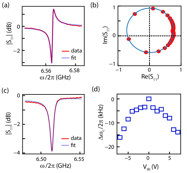
For low temperature measurements, the device is placed inside a light-tight sample box machined from OFHC copper, and mounted to the mixing chamber plate of a dilution refrigerator. A sufficiently attenuated input line is used to drive the cavity. Using a circulator, the reflected signal from the cavity is routed towards a HEMT amplifier at the 4K stage. Between the circulator and the device port, we use a broadband bias-tee, which allows us to add a dc voltage to the input feedline of the cavity. At room temperature, we use a vector network analyzer to record the reflection coefficient of the device. Fig. 2(a) and (b) show the measurement of at 20 mK in the logarithmic and polar format. The asymmetry in the resonance curve arises due to the finite isolation of the circulator that is being used to separate input and output signals. This asymmetry can easily be captured by considering a direct leakage of signal from the input port to the output port. The leakage signal and the signal reflected from the cavity interfere with each other to produce a Fano-lineshape in the response. In the polar format, this effect shows up as a resonance circle with its center shifted away from the x-axis. This interference effect can easily be captured by,
| (1) |
Here is the isolation of the circulator, is the ratio between the external dissipation rate and the total dissipation rate , is the cavity resonant frequency and is the phase-factor arising from the propagation delay. Using this model, we estimated internal and external dissipation rates of 101 kHz and 1.1 MHz, respectively. The extracted circulator-isolation of 15 dB matches close to the value specified by the manufacturer. As shown in Fig. 2(c), the validity of this model is further tested by fitting the measurements of of the cavity at 3 K, reaffirming an external coupling rate of 1.1 MHz.
Due to the placement of the mechanical resonator as a part of the quarter-wavelength cavity, a dc bias at the feedline allows us to apply an electrostatic force on the mechanical resonator, thereby changing its mean position. Fig. 2(d) shows a change in cavity resonance frequency with dc voltage, arising due to the capacitive loading of the cavity-mode. We observe a change of 15 kHz in the cavity resonant frequency with an application of 7 V, corresponding to an estimated displacement of 220 pm in the equilibrium position of the BSCCO resonator.
3.2 Measurement of the mechanical mode
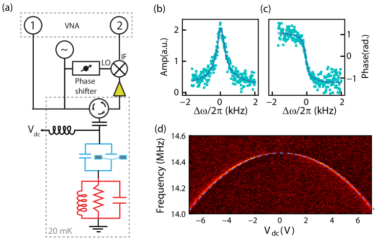
To characterize the mechanical resonator, we use a homodyne measurement scheme as shown in Fig. 3(a). A low-frequency RF signal and a dc signal are sent to the feedline to “electrostatically” apply a force on the mechanical resonator, where is the derivative of flake capacitance with respect to displacement. A microwave tone resonant with cavity frequency is also added to the feedline. The motion of the mechanical resonator phase modulates the reflected signal from the cavity producing two sidebands at . The reflected signal is then demodulated using an external mixer at room temperature. The phase of the LO is adjusted so that the mixed down signal is predominantly in the phase quadrature. This way the cavity is used as an interferometer, and phase modulation due to mechanical motion gets recorded. To avoid any nonlinear mixing between the ac and microwave signals in the amplification chain, we use two bandpass filters (2.9 GHz - 8.7 GHz) before the low temperature amplifier providing 80 dB suppression of ac-signal. The ac-drive and the demodulated signals are controlled and recorded by a vector network analyzer, thereby a measurement of directly relates to the responsivity of the mechanical resonator.
Fig. 3(b) and (c) show the mechanical device response measured at V, along with a fitted curve, giving a resonant frequency of 14.46 MHz, and quality factor of 36620. Application of the dc voltage enables us to change the equilibrium position of the mechanical resonator, and thus changing its resonant frequency. Fig. 3(d) shows a color plot of demodulated signal as the dc voltage and frequency of ac-drive are varied. The sharp changes in color represent the resonant frequency of the mechanical mode, showing a parabolic dependence on . It is worth pointing out here that with the ability to add a coherent mechanical drive in our system, a parametric drive can lead to interesting opto-mechanically-induced transparency regimes [30, 31].
The negative dispersion of mechanical resonant frequency is quite common in electromechanical resonators at low temperatures. It arises from the softening of the mechanical spring constant due to contribution from the electrostatic energy [32]. Assuming a parallel plate geometry, for the mechanical capacitor, the dispersion of resonant frequency can be captured by the following equation of motion,
| (2) |
Here is the radius of the capacitor plate, is the separation between the two plates, is the intrinsic spring constant, and is the total mass of the resonator. It should be noted that due to imperfect clamping, the mode shape could be different from that of an ideal circular drumhead. The choice of the total mass of the resonator leads to an effective amplitude of vibration. The blue dotted line in Fig.3(d) is the calculated dispersion based on the Eq.(2), using only the device geometry parameters.
4 Dissipation in mechanical resonators of BSCCO
4.1 DC-bias dependence of mechanical response
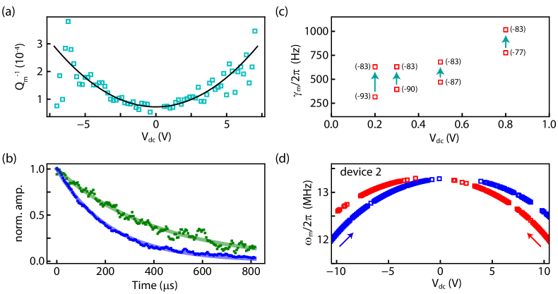
After describing the basic measurement scheme, we investigate the dissipation of mechanical mode in this section. In the devices studied here, we observe a strong dependence of quality factor on . Fig. 4(a) shows the plot of inverse of the quality factor with dc voltage. The dc voltage dependent damping can be attributed to the capacitive-circuit damping originating from the finite contact resistance between BSCCO flake and Mo-Re film. For a fixed dc voltage on the feedline, a vibrating capacitor must shuffle charges to the cavity to balance the current. Any finite contact resistance would lead to a power-dissipation, and hence a loss of the mechanical energy. These losses can be worked out as [33]. The solid line in Fig. 4(a) plots the total loss-rate of the resonator i.e. , where is the intrinsic loss rate of the resonator which includes dissipation due to all the other mechanisms.
To rule out broadening of spectroscopic linewidth by resonator dephasing, we performed measurements of mechanical relaxation rate using time domain techniques. This measurement helps in calculating mechanical energy dissipation by removing the sensitivity to first-order frequency noise, and to the mechanical nonlinearities [34]. For these measurements, a pulse modulated signal is generated to drive the mechanical resonator, and demodulated signal is recorded on a scope. To improve the signal to noise ratio, ten thousand single shot traces were averaged. Fig. 4(b) shows the normalized amplitude traces of ring-downs along with fitted curves at two different dc voltages. The extracted relaxation rates match well with the rates calculated from the spectroscopy measurements, thereby ruling out any significant dephasing of the resonator.
Using the capacitive-circuit damping model (solid line in Fig. 4(a)), we estimate 11.5 k contact resistance between the BSCCO flake and Mo-Re contact. The sensitivity of outer few layers of BSCCO to the ambient conditions is well known, resulting in large contact resistance or even insulating behavior in monolayer samples [12, 35]. The contact resistance value reported here corroborates well with the electron-transport devices fabricated without in-situ etch of first few layers of the BSCCO flake. Effect of contact resistance can also be seen in the dissipation of mechanical energy with change in the power of cavity driving signal used for readout. Due to high contact resistance, the dissipated energy could locally heat the BSCCO at higher cavity power, thus increasing the mechanical damping. As shown in Fig. 4(c), the increase in mechanical linewidth for increasing input power supports this hypothesis over a range of gate voltages.
The effect of contact resistance on mechanical modes reflects severely in thinner mechanical resonators. Fig. 4(d) shows the frequency dispersion from a similar device having 14 nm thick BSCCO mechanical resonator. Hysteresis in resonant frequency is observed with the direction of dc voltage sweep. The hysteresis with respect to sweep direction of dc voltage suggests a larger contact resistance, resulting in a “slower charging” of the BSCCO-capacitor, and hence a longer time for the mechanical oscillator to reach an equilibrium position.
4.2 Temperature dependence of mechanical response
From the previous discussion on dissipation, it is evident that contact resistance at the superconducting interface is degrading the mechanical quality factors of these resonators. It raises an interesting question if the performance of this layered superconductor is limited by resistive heating or by the intrinsic material properties. In the past, resonant ultrasonic spectroscopy techniques have been utilized for the measurements of internal friction and sound velocity in cuprate superconductors, revealing the presence of low energy tunneling states [36, 37].
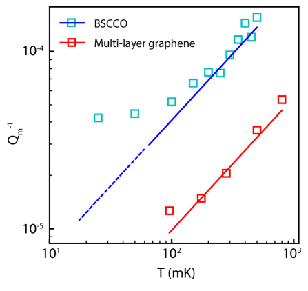
To gain insight into the intrinsic performance of thin BSCCO resonators in the mK range, we record the variations in the mechanical dissipation for different temperatures as shown in Fig. 5. Such a temperature dependence of dissipation, reflecting a saturation at very low temperatures and a power-law dependence above a crossover temperature is quite universal in nano-electro-mechanical resonators of different layered materials [33]. Due to large surface to volume ratio in such systems, the enhanced surface defect density results in low-energy tunneling states [38].
Depending on the energy distribution of the tunneling states, the mechanical dissipation shows a power-law dependence on temperature , with an exponent that can vary from 0 to 3 below a certain crossover temperature. For example, for a broad distribution of energies of tunneling states such as in glasses, dissipation is expected to follow a dependence. Crystals with a low density of defects are expected to show a linear dependence and a saturation at lower temperatures [39]. Phenomenological models such as soft-potential model which predicts an exponent of 0.75, and a saturation below a crossover temperature [40]. It is also worth pointing out that the molecular dynamics simulation of layered materials, studying friction resulting from van der Waals forces between different layers and free edges also predict power-law behavior with exponents varying from 0.3 to 0.9 [41, 42].
The observed behavior of dissipation seems to follow the predictions from a soft-potential model. In Fig. 5, the solid lines are plotted with an exponent of 0.75, serving a guide to the eyes. Similar behavior is observed in multilayer graphene resonator coupled to Mo-Re cavities as shown by red-squares in Fig. 5. While this observation confirms the presence of tunneling states, the observed exponent seems to suggest the presence of soft localized modes. Recently, a linear temperature dependence of dissipation has been observed in a van der Waals hetero-structure of NbSe2 encapsulated by multilayer graphene attributed to the reduced resistive heating in the mechanical resonator [22]. These observations suggest that by improving the electrical contact between BSCCO and Mo-Re surface, the intrinsic performance of BSCCO resonators could be as good as that reported for other multilayer materials. Indeed, by extrapolating the dissipation in BSCCO data, we expect at 10 mK temperature.
5 Conclusions and outlook
To summarize, we have studied the mechanical performance of the exfoliated thin flakes of a high-Tc superconductor BSCCO in the sub-kelvin temperature range, by coupling their motion to a superconducting cavity. These measurements reveal that the mechanical dissipation in these resonators is limited by the contact resistance between the microwave cavity and BSCCO, resulting from the resistive outer layers of the flakes. Temperature dependence of dissipation confirms the presence of tunneling states. In future, these issues can be addressed by exfoliation and transfer of flakes inside a controlled inert atmosphere, which could provide a way for the applications of this material for cavity-optomechanics experiments. Moreover, these techniques can be extended to perform measurements near the superconducting transition temperature or in presence of the magnetic field to gain insight into the microscopics of electron-phonon coupling.
6 References
References
- [1] Castro Neto, A. H., Guinea, F., Peres, N. M. R., Novoselov, K. S., and Geim, A. K. Reviews of Modern Physics 81(1), 109–162 January (2009).
- [2] Castellanos-Gomez, A., Singh, V., van der Zant, H. S. J., and Steele, G. A. Annalen der Physik 527(1-2), 27–44 January (2015).
- [3] Bernardi, M., Ataca, C., Palummo, M., and Grossman, J. C. Nanophotonics 6(2), 479–493 (2016).
- [4] Bunch, J. S., Zande, A. M. v. d., Verbridge, S. S., Frank, I. W., Tanenbaum, D. M., Parpia, J. M., Craighead, H. G., and McEuen, P. L. Science 315(5811), 490–493 January (2007).
- [5] Chen, C., Rosenblatt, S., Bolotin, K. I., Kalb, W., Kim, P., Kymissis, I., Stormer, H. L., Heinz, T. F., and Hone, J. Nat Nano 4(12), 861–867 December (2009).
- [6] Singh, V., Sengupta, S., Solanki, H. S., Dhall, R., Allain, A., Dhara, S., Prita Pant, and Deshmukh, M. M. Nanotechnology 21(16), 165204 (2010).
- [7] Sengupta, S., Solanki, H., Singh, V., Dhara, S., and Deshmukh, M. Physical Review B 82(15), 155432 October (2010).
- [8] Castellanos-Gomez, A., Poot, M., Steele, G. A., van der Zant, H. S. J., Agraït, N., and Rubio-Bollinger, G. Advanced Materials 24(6), 772–775 February (2012).
- [9] Wang, Z., Jia, H., Zheng, X.-Q., Yang, R., Ye, G. J., Chen, X. H., and Feng, P. X.-L. Nano Letters 16(9), 5394–5400 (2016). PMID: 27505636.
- [10] Eichler, A., Moser, J., Chaste, J., Zdrojek, M., Wilson-Rae, I., and Bachtold, A. Nature Nanotechnology 6(6), 339–342 June (2011).
- [11] Singh, V., Shevchuk, O., Blanter, Y. M., and Steele, G. A. Physical Review B 93(24), 245407 June (2016).
- [12] Novoselov, K. S., Jiang, D., Schedin, F., Booth, T. J., Khotkevich, V. V., Morozov, S. V., and Geim, A. K. Proceedings of the National Academy of Sciences of the United States of America 102(30), 10451–10453 July (2005).
- [13] Sandilands, L. J., Shen, J. X., Chugunov, G. M., Zhao, S. Y. F., Ono, S., Ando, Y., and Burch, K. S. Physical Review B 82(6), 064503 August (2010).
- [14] Wang, X., You, L. X., Xie, X. M., Lin, C. T., and Jiang, M. H. Journal of Raman Spectroscopy 43(7), 949–953 December (2011).
- [15] Huang, Y., Sutter, E., Shi, N. N., Zheng, J., Yang, T., Englund, D., Gao, H.-J., and Sutter, P. ACS Nano 9(11), 10612–10620 November (2015).
- [16] Sachdev, S. Reviews of Modern Physics 75(3), 913–932 July (2003).
- [17] Liao, M., Zhu, Y., Zhang, J., Zhong, R., Schneeloch, J., Gu, G., Jiang, K., Zhang, D., Ma, X., and Xue, Q.-K. Nano Letters 18(9), 5660–5665 September (2018).
- [18] Zhao, S. Y. F., Poccia, N., Panetta, M. G., Yu, C., Johnson, J. W., Yoo, H., Zhong, R., Gu, G. D., Watanabe, K., Taniguchi, T., Postolova, S. V., Vinokur, V. M., and Kim, P. arXiv:1809.06944 [cond-mat] September (2018). arXiv: 1809.06944.
- [19] Aspelmeyer, M., Kippenberg, T. J., and Marquardt, F. Reviews of Modern Physics 86(4), 1391–1452 December (2014).
- [20] Singh, V., Bosman, S. J., Schneider, B. H., Blanter, Y. M., Castellanos-Gomez, A., and Steele, G. A. Nature Nanotechnology 9(10), 820–824 October (2014).
- [21] Weber, P., Güttinger, J., Tsioutsios, I., Chang, D. E., and Bachtold, A. Nano Letters 14(5), 2854–2860 May (2014).
- [22] Will, M., Hamer, M., Müller, M., Noury, A., Weber, P., Bachtold, A., Gorbachev, R. V., Stampfer, C., and Güttinger, J. Nano Letters 17(10), 5950–5955 October (2017).
- [23] Shekhter, A., Ramshaw, B. J., Liang, R., Hardy, W. N., Bonn, D. A., Balakirev, F. F., McDonald, R. D., Betts, J. B., Riggs, S. C., and Migliori, A. Nature 498(7452), 75–77 June (2013).
- [24] Varma, C. M. and Zhu, L. Proceedings of the National Academy of Sciences 112(20), 6331–6335 May (2015).
- [25] Jindal, A., Jangade, D. A., Kumar, N., Vaidya, J., Das, I., Bapat, R., Parmar, J., Chalke, B. A., Thamizhavel, A., and Deshmukh, M. M. Scientific Reports 7(1), 3295 June (2017).
- [26] Singh, V., Schneider, B. H., Bosman, S. J., Merkx, E. P. J., and Steele, G. A. Applied Physics Letters 105(22), 222601 December (2014).
- [27] Amet, F., Ke, C. T., Borzenets, I. V., Wang, J., Watanabe, K., Taniguchi, T., Deacon, R. S., Yamamoto, M., Bomze, Y., Tarucha, S., and Finkelstein, G. Science 352(6288), 966–969 May (2016).
- [28] Kroll, J. G., Uilhoorn, W., Enden, K. L. v. d., Jong, D. d., Watanabe, K., Taniguchi, T., Goswami, S., Cassidy, M. C., and Kouwenhoven, L. P. Nature Communications 9(1), 4615 November (2018).
- [29] Castellanos-Gomez, A., Buscema, M., Molenaar, R., Singh, V., Janssen, L., van der Zant, H. S. J., and Steele, G. A. 2D Materials 1(1), 011002 April (2014).
- [30] Zhou, X., Zhang, L., Pang, W., Zhang, H., Yang, Q., and Zhang, D. New Journal of Physics 15(10), 103033 October (2013).
- [31] Lemonde, M.-A., Didier, N., and Clerk, A. A. Nature Communications 7, 11338 April (2016).
- [32] Kozinsky, I., Postma, H. W. C., Bargatin, I., and Roukes, M. L. Applied Physics Letters 88(25), 253101 June (2006).
- [33] Imboden, M. and Mohanty, P. Physics Reports 534(3), 89–146 January (2014).
- [34] Schneider, B. H., Singh, V., Venstra, W. J., Meerwaldt, H. B., and Steele, G. A. Nature Communications 5, 5819 December (2014).
- [35] Sandilands, L. J., Reijnders, A. A., Su, A. H., Baydina, V., Xu, Z., Yang, A., Gu, G., Pedersen, T., Borondics, F., and Burch, K. S. Physical Review B 90(8), 081402 August (2014).
- [36] Esquinazi, P., Luzuriaga, J., Duran, C., Esparza, D. A., and D’Ovidio, C. Physical Review B 36(4), 2316–2318 August (1987).
- [37] Esquinazi, P., Durán, C., Fainstein, C., and Regueiro, M. N. Physical Review B 37(1), 545–547 January (1988).
- [38] Seoánez, C., Guinea, F., and Castro Neto, A. H. Physical Review B 77(12), 125107 March (2008).
- [39] Phillips, W. A. Reports on Progress in Physics 50(12), 1657 (1987).
- [40] Gil, L., Ramos, M. A., Bringer, A., and Buchenau, U. Physical Review Letters 70(2), 182–185 January (1993).
- [41] Kim, S. Y. and Park, H. S. Applied Physics Letters 94(10), 101918 March (2009).
- [42] Takamura, M., Okamoto, H., Furukawa, K., Yamaguchi, H., and Hibino, H. Micromachines 7(9), 158 September (2016).