Signatures of defect-localized charged excitons in the photoluminescence of monolayer molybdenum disulfide
Abstract
We study spatial photoluminescence characteristics of neutral and charged excitons across extended monolayer MoS2 synthesized by chemical vapor deposition. Using two-dimensional hyperspectral photoluminescence mapping at cryogenic temperatures we identify regions with increased emission from charged excitons associated with both spin-orbit split valence subbands. Such regions are attributed to unintentional doping at defect sites with excess charge that bind neutral excitons to form defect-pinned trions. Our findings imply comparable timescales for the formation, relaxation, and radiative decay of trions, and add defect-localized and trions to the realm of photoexcited quasiparticles in layered semiconductors.
Published in Phys. Rev. Materials 2, 124003 (2018). Copyright 2018 American Physical Society.
The version of record is available online at https://doi.org/10.1103/PhysRevMaterials.2.124003.
The photophysics of semiconducting transition metal dichalcogenide (TMD) monolayers (MLs) such as molybdenum disulfide (MoS2) are dominated by excitonic phenomena. The inherently two-dimensional material properties with strong confinement in space and reduced dielectric screening lead to tightly bound electron-hole pairs with binding energies exceeding several hundred of meV He et al. (2014); Chernikov et al. (2014); Ye et al. (2014). The two lowest band-edge excitons, commonly referred to as and excitons, originate from the spin-orbit split valence subbands at the and valleys of the hexagonal Brillouin zone Splendiani et al. (2010); Mak et al. (2010). Due to strong spin-orbit effects and broken inversion symmetry in real space, the exciton spins are pinned to their valley degree of freedom and can be addressed selectively or coherently with polarized light Mak et al. (2012); Zeng et al. (2012); Jones et al. (2013), enabling their manipulation for valleytronic applications Xu et al. (2014); Schaibley et al. (2016). Furthermore, large Coulomb interactions in TMDs give rise to pronounced many-body phenomena where quasiparticles consisting of three or more charge carriers are formed, including trions Mak et al. (2013); Ross et al. (2013); Jones et al. (2013), biexcitons You et al. (2015); Sie et al. (2015); Hao et al. (2017), or Fermi polarons Sidler et al. (2017).
The kinetics responsible for the photogeneration of stable many-body systems are complex Almand-Hunter et al. (2014). For example, in the limit of low densities of excess charge carriers, trions may form through coalescence of an exciton with an extra charge within the Fermi sea or pinned to a defect, or evolve from an electron-hole plasma in a nonequilibrium state Portella-Oberli et al. (2009). In most cases the number of photogenerated trions is determined by the former channel and depends on the doping level of the semiconductor.
In our work we studied electrically and chemically doped ML MoS2 with confocal photoluminescence (PL) spectroscopy at cryogenic temperatures. ML MoS2 crystals were grown by chemical vapor deposition (CVD) as described previously Najmaei et al. (2013); Neumann et al. (2017). After synthesis, the flakes were transferred onto substrates of highly -doped silicon (Si) with nm of thermal silicon dioxide (SiO2). A field-effect transistor (FET) was fabricated for electrostatic doping of one sample. On the second sample grown under identical conditions we studied bare MoS2 flakes without electric contacts yet with local chemical doping effects due to unintentionally formed point defects Hong et al. (2015) which promote adsorption of molecular contaminants Lin et al. (2016); Cai et al. (2016). In the experiments described below we used the FET sample to calibrate the charge polarity of the background doping characteristic of ML MoS2 on SiO2 Radisavljevic et al. (2011); Najmaei et al. (2013) and the associated spectral signatures of and PL stemming from neutral and negatively charged excitons of the exciton manifold Mak et al. (2013); Tongay et al. (2013a); Mouri et al. (2013); Cadiz et al. (2016). In general, the two PL resonances can be ascribed to many-body generalizations of trion bound and unbound states or excitons dressed by the Fermi sea, and represent trions and excitons at sufficiently low carrier densities Efimkin and MacDonald (2017). Based on the reference measurements of the first sample, we used the second sample to study the PL characteristics of neutral and charged excitons of both and spin-orbit split manifolds. Our results identify the emission from defect-localized negatively charged trions, , as excited-state counterparts of the charged exciton. Moreover, from the analysis of the associated charge doping profiles obtained in PL imaging we provide insight into the trion formation dynamics for both exciton manifolds.
Our cryogenic PL spectroscopy and raster-scan imaging experiments were performed in a helium bath cryostat at K or a closed-cycle cryostat with a base temperature of K. The samples were positioned into the focal plane of a low-temperature apochromatic objective with a numerical aperture of and diffraction-limited confocal excitation and detection spots of m diameter. PL and Raman measurements were performed with lasers at nm or nm and a spectrometer equipped with a nitrogen-cooled Si CCD. The spectral resolution of the system was meV for PL and cm-1 for Raman spectroscopy.
First, we studied the effect of intentional doping of MoS2 ML flakes obtained with our sample fabrication method involving CVD and transfer to target substrates Reina et al. (2008). The schematics and an atomic force micrograph of our ML MoS2 FET device are shown in Figs. 1(a) and 1(b), respectively. Electrical contacts on top of a MoS2 ML triangle were defined by means of laser lithography and deposition of titanium ( nm) and gold ( nm). The -doped Si substrate was used as the back gate of the device. The FET exhibited -type conductivity in cryogenic current-voltage measurements [Fig. 1(c)] with non-Ohmic response of the source-drain current that is characteristic of non-annealed devices with sizable Schottky barriers Radisavljevic et al. (2011); Buscema et al. (2013); Yamaguchi et al. (2015).
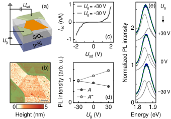
The tuning of the doping profile in the low carrier density regime with negligible screening effects was also monitored with PL spectroscopy. For MoS2 MLs on SiO2 both neutral excitons and negative trions with a splitting of meV, corresponding to the trion binding energy, contribute to the emission spectrum Mak et al. (2013); Cadiz et al. (2016). In Fig. 1(d) we plot the and PL intensities as a function of the applied gate voltage. The data points were obtained from spectral deconvolution of the total PL spectrum into the emission from and excitons, each modeled by a Lorentzian with full-width at half-maximum (FWHM) linewidth of meV and peak maxima separated by the trion binding energy [Fig. 1(e); note the correspondence between the spectrum in blue and the model fit in green]. For zero gate bias the imbalanced intensities of and correspond to an electron doping density on the order of cm-2 Lee et al. (2014) due to substrate-induced background doping of MoS2 on SiO2 Dolui et al. (2013); Scheuschner et al. (2014); Kang and Han (2017). An increase in the electron concentration at a gate voltage of V was accompanied by an increase of and a decrease of emission and the opposite effect was observed at V [Fig. 1(d)] in accord with a partial compensation of the negative background doping at negative gate voltages.
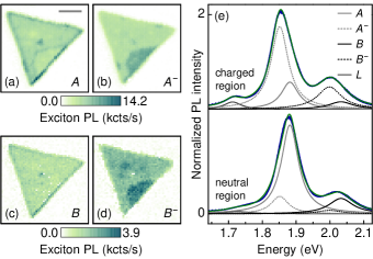
Complementary to field-effect doping, chemical doping provides an alternative approach to trion generation in ML TMDs Mouri et al. (2013); Peimyoo et al. (2014); Lui et al. (2014). Molecular adsorption and defect sites in layered semiconductors give rise to binding of excitons to immobile charges Tongay et al. (2013b); Nan et al. (2014), thereby forming defect-localized trions. In this regime of localized excitonic complexes Godde et al. (2016), we expand our analysis to a previously studied MoS2 single crystal Neumann et al. (2017) without active charge control from the same CVD batch as the sample of Fig. 1. By raster scanning the sample with respect to diffraction-limited confocal excitation and detection spots, PL spectra spanning the range of and excitons were recorded. At each pixel of the raster scans the spectra were decomposed into five Lorentzians. Four distributions with fixed energies and linewidths were used to fit and excitons and their trion counterparts and Berkelbach et al. (2013), and lower energy localized excitons were accounted for by an additional Lorentzian with variable peak energy and linewidth parameters. These conditions restrict the validity of our evaluation to low charge doping of cm-2, where the exciton-trion peak difference is approximately constant Chernikov et al. (2015); Courtade et al. (2017) and the picture of dressed exciton states is not relevant Efimkin and MacDonald (2017). Results for and excitons and trions are shown in Figs. 2(a)–2(d). The observation of excitons in PL indicates that relaxation pathways from the to the exciton manifold which require spin or valley flips of both electrons and holes Xiao et al. (2012) are slow as compared to the radiative exciton recombination time.
For direct comparison, Fig. 2(e) shows representative spectra exhibiting mostly neutral and charged excitons in the MoS2 ML (note the increased emission from localized excitons in the trion-dominated spectrum suggesting local correlations between trion peak intensity and disorder). Best fits for excitons at eV and excitons at eV were obtained with inhomogeneously broadened FWHM linewidths of meV and meV, respectively, and the same linewidths for the corresponding trions. Our analysis verifies that the negatively charged trion counterpart to is also stable Berkelbach et al. (2013) with a slightly larger trion binding energy of meV. The small difference in the trion binding suggests comparable extends of the Bohr radii for and trions, consistent with diamagnetic shifts of neutral and excitons in the related ML material WS2 Stier et al. (2016). Our findings of luminescent trions complement their observation in reflectance contrast measurements in ML WS2 Chernikov et al. (2015) as well as in photoinduced absorption of few-layer MoS2 Borzda et al. (2015).
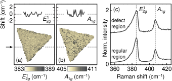
Apart from charge doping, ML spectra are also known to be sensitive to strain He et al. (2013); Conley et al. (2013); Zhu et al. (2013). To eliminate any related ambiguity in the origin of spectral shifts of and -type excitons, we inspected the crystal structure of the MoS2 flake in Fig. 2 by means of Raman spectroscopy. Vibrational in-plane modes in TMDs such as the mode are most affected by strain. In MLs the Raman shift of the mode is known to decrease by cm-1 per percent of uniaxial strain Rice et al. (2013) without dependence on charge doping Chakraborty et al. (2012). For our sample the homogenous profile of the mode around cm-1 shown in Fig. 3(a) suggests strain variations across the crystal of at most %. These variations can only account for exciton redshifts of less than half of the measured binding energies of and trions. Opposed to vibrations, the frequency of the out-of-plane mode is not sensitive to uniaxial strain Rice et al. (2013) but softens from charge neutrality to an electron doping density of cm-2 by cm-1 Chakraborty et al. (2012). Fig. 3(b) shows the spatial distribution of the frequency centered at cm-1 for our ML crystal. The profile reveals uniformity within cm-1 and an average to peak separation of cm-1 that is typical for CVD-grown MoS2 MLs at cryogenic temperatures Lanzillo et al. (2013). With this data at hand, we confirm that the flake exhibited only low doping well below the electron concentration of cm-2 with local changes bordering the sensitivity of our experiment. In fact, high signal-to-noise Raman spectra of the and modes at representative chemically doped and regular ML positions of the flake were identical within our resolution limit [Fig. 3(c)]. We therefore conclude that the MoS2 ML is weakly and locally doped without substantial strain changes.
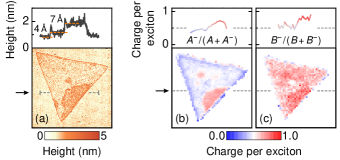
Further support in favor of defect-pinned doping was obtained by mapping the surface topography of the crystal [Fig. 4(a)]. Apart from regular ML domains identified by the step of Å above the substrate, our measurements clearly show regions elevated by Å on top of the ML, such as the trion-rich puddle at the lower edge. We assume that these elevated regions stem from accumulations of molecular adsorbates at negatively charged sulfur vacancy sites Qiu et al. (2013), which are commonly encountered in CVD-grown MoS2 due to their low formation energy Zhou et al. (2013). The correspondence in the observation of and trions at the same positions implies that the localized electronic charges of sulfur vacancies were not fully screened by the molecules acting as acceptors.
Finally, we qualitatively discuss local charge inhomogeneities in the chemically doped MoS2 ML using the ratio of densities of charged to neutral excitons. To this end, we compute charge doping profiles as for the ground state excitons and for the spin-orbit split excitons [Figs. 4(b) and 4(c), respectively]. The profiles highlight in red (blue) local regions with higher (lower) electron concentrations, among them the surface-contaminated puddle. At regular positions away from the puddle and edges, the charge concentration of electrons per -type exciton [Fig. 4(b)] is found in good agreement with the background doping of our electrostatically tunable ML at zero gate voltage [Fig. 1(d)]. In the limit of low doping, and assuming trion formation through exciton-electron Coulomb interactions on timescales fast compared to the exciton decay time , the profiles provide a quantitative means to image the local doping level by employing the mass action model Ross et al. (2013); Mouri et al. (2013); Peimyoo et al. (2014). However, considering that PL decay typically occurs within only a few picoseconds for Korn et al. (2011); Lagarde et al. (2014); Cadiz et al. (2016) and Palummo et al. (2015) complexes at low temperatures, it is likely that and trion formation is slow enough to compete with the population decay of the trion unbound states on comparable timescales in our CVD-grown sample. This is indeed in accord with measured trion formation times of ps in MoS2 Lui et al. (2014) and ps in MoSe2 Singh et al. (2016). A quantitative model of the local doping concentration thus requires explicit knowledge of timescales for charge carrier capture and population decay not measured for our samples. At the qualitative level, the comparison of the maps in Figs. 4(b) and 4(c) demonstrates that and trion photogeneration dynamics are not too distinct. In other words, exciton population relaxes on timescales comparable to their radiative decay, providing sufficient time for the formation of defect-localized trions. The reduced contrast and increased values of charged exciton densities in the doping profile of Fig. 4(c) indicate for our sample that the ratio between the timescales of trion formation and neutral exciton decay () is smaller for the manifold as compared to the manifold. This observation is most pronounced for trions in regular regions with low contamination.
In summary, spatially inhomogeneous distributions of charged excitons due to unintentional chemical doping were studied on CVD-grown MoS2 MLs with PL imaging and spectroscopy. In addition to trions, our PL experiments identified defect-localized trions with binding energy of meV. Our analysis of charge doping profiles constructed from relative contributions of charged and neutral exciton PL indicates that the formation of localized trions competes with their relaxation and decay on comparable timescales.
We thank P. Altpeter and R. Rath for assistance in the clean room. This research was funded by the European Research Council under the ERC grant agreement no. 336749, the Volkswagen Foundation, the Deutsche Forschungsgemeinschaft (DFG) Cluster of Excellence Nanosystems Initiative Munich (NIM) with financial support from the Center for NanoScience (CeNS) and LMUinnovativ. A.D.M. and H.Y. acknowledge support from the Laboratory Directed Research and Development (LDRD) program and the Center for Integrated Nanotechnologies at LANL.
References
- He et al. (2014) K. He, N. Kumar, L. Zhao, Z. Wang, K. F. Mak, H. Zhao, and J. Shan, Phys. Rev. Lett. 113, 026803 (2014).
- Chernikov et al. (2014) A. Chernikov, T. C. Berkelbach, H. M. Hill, A. Rigosi, Y. Li, O. B. Aslan, D. R. Reichman, M. S. Hybertsen, and T. F. Heinz, Phys. Rev. Lett. 113, 076802 (2014).
- Ye et al. (2014) Z. Ye, T. Cao, K. O’Brien, H. Zhu, X. Yin, Y. Wang, S. G. Louie, and X. Zhang, Nature 513, 214 (2014).
- Splendiani et al. (2010) A. Splendiani, L. Sun, Y. Zhang, T. Li, J. Kim, C.-Y. Chim, G. Galli, and F. Wang, Nano Lett. 10, 1271 (2010).
- Mak et al. (2010) K. F. Mak, C. Lee, J. Hone, J. Shan, and T. F. Heinz, Phys. Rev. Lett. 105, 136805 (2010).
- Mak et al. (2012) K. F. Mak, K. He, J. Shan, and T. F. Heinz, Nat. Nanotechnol. 7, 494 (2012).
- Zeng et al. (2012) H. Zeng, J. Dai, W. Yao, D. Xiao, and X. Cui, Nat. Nanotechnol. 7, 490 (2012).
- Jones et al. (2013) A. M. Jones, H. Yu, N. J. Ghimire, S. Wu, G. Aivazian, J. S. Ross, B. Zhao, J. Yan, D. G. Mandrus, D. Xiao, et al., Nat. Nanotechnol. 8, 634 (2013).
- Xu et al. (2014) X. Xu, W. Yao, D. Xiao, and T. F. Heinz, Nat. Phys. 10, 343 (2014).
- Schaibley et al. (2016) J. R. Schaibley, H. Yu, G. Clark, P. Rivera, J. S. Ross, K. L. Seyler, W. Yao, and X. Xu, Nat. Rev. Mater. 1, 16055 (2016).
- Mak et al. (2013) K. F. Mak, K. He, C. Lee, G. H. Lee, J. Hone, T. F. Heinz, and J. Shan, Nat. Mater. 12, 207 (2013).
- Ross et al. (2013) J. S. Ross, S. Wu, H. Yu, N. J. Ghimire, A. M. Jones, G. Aivazian, J. Yan, D. G. Mandrus, D. Xiao, W. Yao, et al., Nat. Commun. 4, 1474 (2013).
- You et al. (2015) Y. You, X.-X. Zhang, T. C. Berkelbach, M. S. Hybertsen, D. R. Reichman, and T. F. Heinz, Nat. Phys. 11, 477 (2015).
- Sie et al. (2015) E. J. Sie, A. J. Frenzel, Y.-H. Lee, J. Kong, and N. Gedik, Phys. Rev. B 92, 125417 (2015).
- Hao et al. (2017) K. Hao, J. F. Specht, P. Nagler, L. Xu, K. Tran, A. Singh, C. K. Dass, C. Schüller, T. Korn, M. Richter, et al., Nat. Commun. 8, 15552 (2017).
- Sidler et al. (2017) M. Sidler, P. Back, O. Cotlet, A. Srivastava, T. Fink, M. Kroner, E. Demler, and A. Imamoglu, Nat. Phys. 13, 255 (2017).
- Almand-Hunter et al. (2014) A. E. Almand-Hunter, H. Li, S. T. Cundiff, M. Mootz, M. Kira, and S. W. Koch, Nature 506, 471 (2014).
- Portella-Oberli et al. (2009) M. T. Portella-Oberli, J. Berney, L. Kappei, F. Morier-Genoud, J. Szczytko, and B. Deveaud-Plédran, Phys. Rev. Lett. 102, 096402 (2009).
- Najmaei et al. (2013) S. Najmaei, Z. Liu, W. Zhou, X. Zou, G. Shi, S. Lei, B. I. Yakobson, J.-C. Idrobo, P. M. Ajayan, and J. Lou, Nat. Mater. 12, 754 (2013).
- Neumann et al. (2017) A. Neumann, J. Lindlau, L. Colombier, M. Nutz, S. Najmaei, J. Lou, A. D. Mohite, H. Yamaguchi, and A. Högele, Nat. Nanotechnol. 12, 329 (2017).
- Hong et al. (2015) J. Hong, Z. Hu, M. Probert, K. Li, D. Lv, X. Yang, L. Gu, N. Mao, Q. Feng, L. Xie, et al., Nat. Commun. 6, 6293 (2015).
- Lin et al. (2016) Z. Lin, B. R. Carvalho, E. Kahn, R. Lv, R. Rao, H. Terrones, M. A. Pimenta, and M. Terrones, 2D Mater. 3, 022002 (2016).
- Cai et al. (2016) Y. Cai, H. Zhou, G. Zhang, and Y.-W. Zhang, Chem. Mater. 28, 8611 (2016).
- Radisavljevic et al. (2011) B. Radisavljevic, A. Radenovic, J. Brivio, V. Giacometti, and A. Kis, Nat. Nanotechnol. 6, 147 (2011).
- Tongay et al. (2013a) S. Tongay, J. Zhou, C. Ataca, J. Liu, J. S. Kang, T. S. Matthews, L. You, J. Li, J. C. Grossman, and J. Wu, Nano Lett. 13, 2831 (2013a).
- Mouri et al. (2013) S. Mouri, Y. Miyauchi, and K. Matsuda, Nano Lett. 13, 5944 (2013).
- Cadiz et al. (2016) F. Cadiz, S. Tricard, M. Gay, D. Lagarde, G. Wang, C. Robert, P. Renucci, B. Urbaszek, and X. Marie, Appl. Phys. Lett. 108, 251106 (2016).
- Efimkin and MacDonald (2017) D. K. Efimkin and A. H. MacDonald, Phys. Rev. B 95, 035417 (2017).
- Reina et al. (2008) A. Reina, H. Son, L. Jiao, B. Fan, M. S. Dresselhaus, Z. Liu, and J. Kong, J. Phys. Chem. C 112, 17741 (2008).
- Buscema et al. (2013) M. Buscema, M. Barkelid, V. Zwiller, H. S. J. van der Zant, G. A. Steele, and A. Castellanos-Gomez, Nano Lett. 13, 358 (2013).
- Yamaguchi et al. (2015) H. Yamaguchi, J.-C. Blancon, R. Kappera, S. Lei, S. Najmaei, B. D. Mangum, G. Gupta, P. M. Ajayan, J. Lou, M. Chhowalla, et al., ACS Nano 9, 840 (2015).
- Lee et al. (2014) C.-H. Lee, G.-H. Lee, A. M. van der Zande, W. Chen, Y. Li, M. Han, X. Cui, G. Arefe, C. Nuckolls, T. F. Heinz, et al., Nat. Nanotechnol. 9, 676 (2014).
- Dolui et al. (2013) K. Dolui, I. Rungger, and S. Sanvito, Phys. Rev. B 87, 165402 (2013).
- Scheuschner et al. (2014) N. Scheuschner, O. Ochedowski, A.-M. Kaulitz, R. Gillen, M. Schleberger, and J. Maultzsch, Phys. Rev. B 89, 125406 (2014).
- Kang and Han (2017) Y. Kang and S. Han, Nanoscale 9, 4265 (2017).
- Peimyoo et al. (2014) N. Peimyoo, W. Yang, J. Shang, X. Shen, Y. Wang, and T. Yu, ACS Nano 8, 11320 (2014).
- Lui et al. (2014) C. H. Lui, A. J. Frenzel, D. V. Pilon, Y.-H. Lee, X. Ling, G. M. Akselrod, J. Kong, and N. Gedik, Phys. Rev. Lett. 113, 166801 (2014).
- Tongay et al. (2013b) S. Tongay, J. Suh, C. Ataca, W. Fan, A. Luce, J. S. Kang, J. Liu, C. Ko, R. Raghunathanan, J. Zhou, et al., Sci. Rep. 3, 2657 (2013b).
- Nan et al. (2014) H. Nan, Z. Wang, W. Wang, Z. Liang, Y. Lu, Q. Chen, D. He, P. Tan, F. Miao, X. Wang, et al., ACS Nano 8, 5738 (2014).
- Godde et al. (2016) T. Godde, D. Schmidt, J. Schmutzler, M. Aßmann, J. Debus, F. Withers, E. M. Alexeev, O. Del Pozo-Zamudio, O. V. Skrypka, K. S. Novoselov, et al., Phys. Rev. B 94, 165301 (2016).
- Berkelbach et al. (2013) T. C. Berkelbach, M. S. Hybertsen, and D. R. Reichman, Phys. Rev. B 88, 045318 (2013).
- Chernikov et al. (2015) A. Chernikov, A. M. van der Zande, H. M. Hill, A. F. Rigosi, A. Velauthapillai, J. Hone, and T. F. Heinz, Phys. Rev. Lett. 115, 126802 (2015).
- Courtade et al. (2017) E. Courtade, M. Semina, M. Manca, M. M. Glazov, C. Robert, F. Cadiz, G. Wang, T. Taniguchi, K. Watanabe, M. Pierre, et al., Phys. Rev. B 96, 085302 (2017).
- Xiao et al. (2012) D. Xiao, G.-B. Liu, W. Feng, X. Xu, and W. Yao, Phys. Rev. Lett. 108, 196802 (2012).
- Stier et al. (2016) A. V. Stier, K. M. McCreary, B. T. Jonker, J. Kono, and S. A. Crooker, Nat. Commun. 7, 10643 (2016).
- Borzda et al. (2015) T. Borzda, C. Gadermaier, N. Vujicic, P. Topolovsek, M. Borovsak, T. Mertelj, D. Viola, C. Manzoni, E. A. A. Pogna, D. Brida, et al., Adv. Funct. Mater. 25, 3351 (2015).
- He et al. (2013) K. He, C. Poole, K. F. Mak, and J. Shan, Nano Lett. 13, 2931 (2013).
- Conley et al. (2013) H. J. Conley, B. Wang, J. I. Ziegler, R. F. Haglund, S. T. Pantelides, and K. I. Bolotin, Nano Lett. 13, 3626 (2013).
- Zhu et al. (2013) C. R. Zhu, G. Wang, B. L. Liu, X. Marie, X. F. Qiao, X. Zhang, X. X. Wu, H. Fan, P. H. Tan, T. Amand, et al., Phys. Rev. B 88, 121301 (2013).
- Rice et al. (2013) C. Rice, R. J. Young, R. Zan, U. Bangert, D. Wolverson, T. Georgiou, R. Jalil, and K. S. Novoselov, Phys. Rev. B 87, 081307 (2013).
- Chakraborty et al. (2012) B. Chakraborty, A. Bera, D. V. S. Muthu, S. Bhowmick, U. V. Waghmare, and A. K. Sood, Phys. Rev. B 85, 161403 (2012).
- Lanzillo et al. (2013) N. A. Lanzillo, A. Glen Birdwell, M. Amani, F. J. Crowne, P. B. Shah, S. Najmaei, Z. Liu, P. M. Ajayan, J. Lou, M. Dubey, et al., Appl. Phys. Lett. 103, 093102 (2013).
- Qiu et al. (2013) H. Qiu, T. Xu, Z. Wang, W. Ren, H. Nan, Z. Ni, Q. Chen, S. Yuan, F. Miao, F. Song, et al., Nat. Commun. 4, 2642 (2013).
- Zhou et al. (2013) W. Zhou, X. Zou, S. Najmaei, Z. Liu, Y. Shi, J. Kong, J. Lou, P. M. Ajayan, B. I. Yakobson, and J.-C. Idrobo, Nano Lett. 13, 2615 (2013).
- Korn et al. (2011) T. Korn, S. Heydrich, M. Hirmer, J. Schmutzler, and C. Schüller, Appl. Phys. Lett. 99, 102109 (2011).
- Lagarde et al. (2014) D. Lagarde, L. Bouet, X. Marie, C. R. Zhu, B. L. Liu, T. Amand, P. H. Tan, and B. Urbaszek, Phys. Rev. Lett. 112, 047401 (2014).
- Palummo et al. (2015) M. Palummo, M. Bernardi, and J. C. Grossman, Nano Lett. 15, 2794 (2015).
- Singh et al. (2016) A. Singh, G. Moody, K. Tran, M. E. Scott, V. Overbeck, G. Berghäuser, J. Schaibley, E. J. Seifert, D. Pleskot, N. M. Gabor, et al., Phys. Rev. B 93, 041401 (2016).