Opto-valleytronic imaging of atomically thin semiconductors
1Fakultät für Physik, Munich Quantum Center, and Center for NanoScience (CeNS),
Ludwig-Maximilians-Universität München, D-80539 München, Germany
2MPA-11 Materials Synthesis and Integrated Devices, Materials Physics and Applications Division,
Los Alamos National Laboratory (LANL), Los Alamos, NM 87545, U.S.A.
3Department of Materials Science and NanoEngineering, Rice University, Houston, TX 77005, U.S.A.
Transition metal dichalcogenide semiconductors represent elementary components of layered heterostructures for emergent technologies beyond conventional opto-electronics. In their monolayer form they host electrons with quantized circular motion and associated valley polarization and valley coherence as key elements of opto-valleytronic functionality. Here, we introduce two-dimensional polarimetry as means of direct imaging of the valley pseudospin degree of freedom in monolayer transition metal dichalcogenides. Using MoS2 as a representative material with valley-selective optical transitions, we establish quantitative image analysis for polarimetric maps of extended crystals, and identify valley polarization and valley coherence as sensitive probes of crystalline disorder. Moreover, we find site-dependent thermal and non-thermal regimes of valley-polarized excitons in perpendicular magnetic fields. Finally, we demonstrate the potential of wide-field polarimetry for rapid inspection of opto-valleytronic devices based on atomically thin semiconductors and heterostructures.
Published in Nature Nanotechnology 12, 329–334 (2017).
The version of record is available online at https://doi.org/10.1038/nnano.2016.282.
The valley quantum degree of freedom manifests itself as the quantized angular motion of crystal electrons near the band edges. In analogy to spin it represents a resource for quantum information in conventional semiconductors such as aluminum arsenide 1 and silicon 2, or in atomically thin materials including graphene 3 and TMDs 4, 5. Direct band-gap monolayer TMDs 6, 7 are particularly viable for practical realizations of valleytronic concepts as they enable initialization 4, manipulation 8 and detection 9, 10, 11 of the valley pseudospin by all-optical means. Despite successful realization of first opto-valleytronic devices 12, 13, controversy prevails with respect to possible intrinsic and extrinsic origins of significant variations in the degrees of valley polarization 9, 10, 11, 14, 15 and valley coherence 16, 17 observed for different material representatives of monolayer TMD semiconductors.
The valley pseudospin in TMDs is most conveniently accessed with photoluminescence (PL) polarimetry of band-edge excitons 5. The degrees of circular and linear PL polarization, and , defined as the ratio of emission intensities detected in co-polarized () and cross-polarized () configurations with a circularly () or linearly () polarized excitation laser, are direct measures of valley polarization 9, 10, 11 and valley coherence 16, 17. Most values reported for circular and linear PL polarizations in monolayer TMDs are well below unity, and they vary significantly with material quality or the underlying substrate 9, 10, 11, 14, 15, 18, 19, 20. A detailed understanding of the variations in and has been elusive to date and partly attributed to different ratios of the exciton and valley dynamics in different samples. Analogous to optical spin orientation 21, ideal initialization of the valley polarization yields in a steady-state PL measurement close to unity if the exciton lifetime is short as compared to the longitudinal valley decay time . The same argument holds for as a measure of valley coherence with the transverse valley decay time . For TMD monolayers with long-lived excitons, one therefore expects a sizable reduction in the degrees of circular and linear polarizations due to exchange-mediated valley decay and dephasing 22, 23, 24 active during the exciton lifetime.
In the following we demonstrate that the notion of the degrees of circular and linear polarization as being determined simply by the exciton and valley lifetimes is of limited validity, and therefore previous quantitative conclusions drawn from this simplistic picture should be critically revised. However, the model is helpful for a qualitative interpretation of varying degrees of valley polarization and coherence across single TMD monolayers. A more quantitative analysis can be provided by taking into account the optical valley initialization processes. This insight is based on our experiments on extended MoS2 flakes grown by chemical vapor deposition (CVD) and transferred onto SiO2/Si substrates as a representative TMD material system (see the Supplementary Information for sample details). The valley pseudospin physics in single- and poly-crystalline MoS2 monolayers were addressed with steady-state two-dimensional circular and linear PL polarimetry.
Photoluminescence spectroscopy of extended monolayers
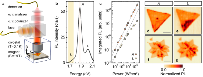
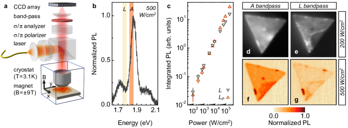
We begin our studies by characterizing individual MoS2 crystals with cryogenic PL. The experimental setup for confocal PL spectroscopy and raster-scan imaging is shown schematically in Fig. 1a. The sample was cooled to K in a closed-cycle cryostat and positioned within the confocal excitation and detection spots of a low-temperature apochromatic objective. The polarization of the excitation and detection pathways was set independently for circular or linear polarimetry by according combinations of linear polarizers, half- and quarter-waveplates. A superconducting solenoid was used to apply magnetic fields up to T perpendicular to the sample.
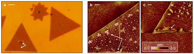
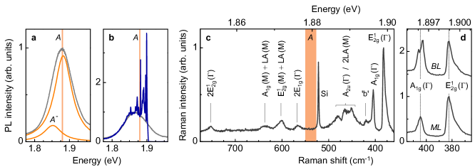
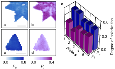
A representative cryogenic spectrum of monolayer MoS2 recorded with a non-resonant excitation laser at nm is shown in Fig. 1b. It features and exciton PL around eV and eV characteristic of monolayer MoS2 on SiO2 6, 7. Additionally, we observed a red-shifted PL of localized excitons () which exhibit saturation as a function of the excitation laser power 25 in contrast to excitons with linear response (Fig. 1c). The maps in Fig. 1d - g, constructed by color-coding normalized raster-scan PL within exciton-specific bands indicated in Fig. 1b, show the and exciton PL profiles for two representative MoS2 flakes of our studies. The triangular shape (Fig. 1d and e) is typical for CVD-grown single-crystal flakes, while the star-shaped geometry of the poly-crystalline flake (Fig. 1f and g) reflects a cluster of single-crystal domains separated by grain boundaries 26, 27.
The PL intensity profiles show spatial variations across the flakes due to the presence of spatial inhomogeneities in the crystal quality. The edges and the center of the single-crystal triangle exhibit a more intense exciton PL than the rest of the flake (Fig. 1d), while the exciton emission is most intense in a ’puddle’ at the right edge of the triangle (Fig. 1e). Based on previous studies 26, 27, Raman spectroscopy (see the Supplementary Information) and optical inspection of other flakes on our sample, we identify the central region as a bilayer triangle formed on top of the monolayer single-crystal MoS2. The puddle is likely a collection of point defect contaminants responsible for exciton localization 25. The poly-crystalline star shows homogeneous domains of both and emission separated by lines of enhanced intensity (Fig. 1f and g) at the grain boundaries 26, 27 which also seem to favor exciton localization. At low excitation powers, emission hot-spots of cryogenic quantum dots 28, 29, 30, 31 dominate the PL intensity profiles of excitons (see the Supplementary Information).
Raster-scan opto-valleytronic imaging
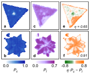
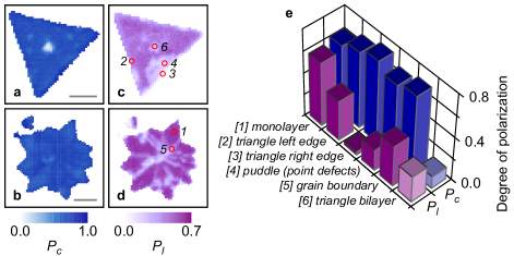
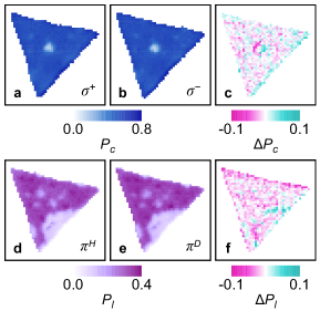
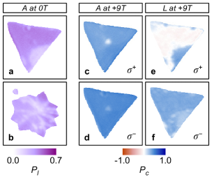
The polarization-resolving feature of our setup allows us to identify characteristic signatures of crystal defects with circular and linear polarimetry. The two-dimensional maps of the degrees of circular and linear PL polarizations in Fig. 2a - d were recorded for the flakes of Fig. 1 with a laser at nm in resonance with the blue shoulder of the exciton PL which typically results in high near-resonant polarization values 10, 16, 32, 15. In the absence of an external magnetic field, time-reversal symmetry implies identical degrees of and valley polarization and thus equal recorded with and polarimetry 4. Equivalently, the valley coherence is independent of the choice of the linear basis 16 (see the Supplementary Information for the equivalence of complementary bases at zero magnetic field). First, we focus our analysis on the fundamental exciton to discuss the polarization in the valley, and the valley coherence in terms of - superpositions.
The feature of highest contrast in the maps of the single- and poly-crystalline flakes is located at the triangle center (Fig. 2a) and coincides with the bilayer region discussed earlier. Optical selection rules are different for TMD bilayers 33 and provide direct means to single out bilayer regions in polarimetric imaging. Away from bilayer regions and edges, the degree of in Fig. 2a and b is remarkably high and homogeneous. Most surprisingly, the grain boundaries of the poly-crystalline star are almost invisible in the map of Fig. 2b. This observation of homogeneous valley polarization is in stark contrast to the sizable variations in the PL intensity profiles (Fig. 1d and f). It is also strongly contrasted by the pronounced inhomogeneities of the respective profiles in Fig. 2c and d, where both the puddle and the grain boundaries appear most prominently as sites of low valley coherence. To discuss these differences qualitatively, we recall the simple model where valley depolarization and dephasing are responsible for the reduction of and during the exciton lifetime. High values in the maps of Fig. 2a and b imply that the degree of optical valley pseudospin initialization is high in our experiments – a necessary condition for the optical generation of valley coherence. With the exception of the bilayer region, the homogenous profiles also suggest that the longitudinal valley relaxation is slow on the timescale of the exciton lifetime even in the presence of disorder. On the same timescale, however, rapid transverse valley relaxation results in locally reduced values as in the defective regions of the flakes in Fig. 2c and d.
In order to visualize the regions of rapid valley dephasing signified by large differences in and , we present differential polarization profiles for both representative flakes. Fig. 2e and f were computed with a scaling factor of and , respectively, to enhance the map contrast and thus the visibility of monolayer defects by highlighting bilayers in green and sites of valley decoherence (crystal edges, grain boundaries and the puddle of surface contaminants) in orange. Orange regions of disorder are characterized by rapid dephasing of optically generated quantum coherent superpositions of and excitons without signatures of low valley polarization. The white areas of the differential profiles in Fig. 2e and f identify the least defective monolayer crystals most favorable for opto-valleytronic applications.
Opto-valleytronic imaging in magnetic field
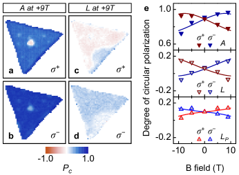
Our analysis is complemented by circular polarimetric profiling in non-zero magnetic fields. A positive magnetic field oriented orthogonal to the TMD monolayer plane breaks the time-reversal symmetry and lifts the valley degeneracy by decreasing (increasing) the exciton energy in the () valley 34, 35, 36, 37, 38, 39. Moreover, it changes the degree of circular polarization 34, 35, 36, 37, 38, which we monitored for our flakes with magneto-optical polarimetry. The polarimetric maps recorded in a magnetic field of T within the and exciton bands are shown in Fig. 3a - d for the representative single-crystal triangle (see the Supplementary Information for complementary measurements in a magnetic field of T). The main signature of the valley Zeeman effect in opto-valleytronic imaging is the field-induced difference in measured with and excitations (compare Fig. 3a and c with b and d). In a positive field of T the within both and spectral bands exhibits a decrease (increase) under () excitation in regular regions of the triangular flake.
To analyze the field-induced changes in the valley polarization of excitons we removed the contribution of the trion PL from the exciton band by spectral deconvolution (see the Supplementary Information). The resulting evolution of with magnetic field on a regular site of the single-crystal triangle is presented in the upper and central panels of Fig. 3e for the deconvolved exciton and for the exciton band, respectively. The data in the upper panel of Fig. 3e exhibit an evolution similar to excitons in WSe2 monolayer 36 with an -shaped pattern that can be much less pronounced on different samples and under less resonant excitation 38. This -shape is not a generic feature of TMD magnetoluminescence as it is distinct from the evolutions of MoSe2 neutral excitons in magnetic field37, 38. It rather reflects a counter-intuitive steady-state distribution of excitons among the two Zeeman-split and valleys 36: at positive magnetic fields the population in the energetically higher valley Zeeman branch becomes progressively protected from the relaxation into the lower branch with increasing magnetic field. This ’hot’ valley exciton population on a regular position is contrasted by the ’thermal’ distribution of excitons in the puddle (Fig. 3e, lower panel) with a sign reversal of the -pattern as one would expect for a population redistribution that favors the exciton state of lowest energy.
The scheme of non-thermal, optically induced valley population imbalance is the opto-valleytronic counterpart of optical spin orientation in conventional semiconductors 21. For the fundamental exciton, rate-equation analysis 36 suggests that out-of-equilibrium and valley populations result from both a finite branching of the optically excited valley polarization into valley flipping and conserving relaxation channels and a slow valley depolarization in the exciton ground state. In fact, valley depolarization times much longer than the exciton decay time underpin the non-thermal valley population regime 36. Our analysis that accounts for inter-valley thermalization in addition to finite branching of the photoexcited population yields best fits to the data (solid lines in Fig. 3e) with for and for and excitons (see the Supplementary Information for model details and other relevant fit parameters). In contrast, the model with ideal initial polarization of the luminescent exciton states predicts for and for excitons, respectively. The discrepancies stem from the ignorance of the idealized model to the details of the valley pseudospin initialization in and exciton ground states. Actually it holds only if the valley conserving relaxation significantly outcompetes the valley flipping relaxation during the formation process of the and excitons out of the selectively excited valley as in the case of excitons in our experiment with near-resonant excitation. This does not apply to localized states, where significant population branching occurs upon relaxation, and different branching scenarios determine the non-thermal and thermal populations of and excitons: for the former, alike for excitons, the valley polarization is increasingly accumulated in the photoexcited upper valley due to a reduction of branching with magnetic field, while for the the latter defect-assisted relaxation likely renders the branching field-independent.
The regime of identified by our analysis for both and excitons in monolayer MoS2 yields upper bounds on the longitudinal valley depolarization times of ps for and ps for and excitons if we take the PL decay time of ps for both the excitons in MoS2 15 and the dominant decay timescale of localized excitons in our sample (see the Supplementary Information for time-resolved PL data). In absolute terms, the longitudinal depolarization time of excitons might be shorter if scaled to a more rapid exciton decay potentially present in our CVD-grown MoS2 flakes but inaccessible in our experiments due to limited temporal resolution. In relative terms, however, our finding of is in accord with previous results on WSe2 36. At the same time it is contrasted by the theoretical estimate ps for the valley depolarization dynamics in the presence of long-range exchange 23, 24 which in turn is an integral part of the finite-branching model 36. This caveat is qualitatively resolved by the notion of exchange-mediated valley depolarization timescales beyond ps for luminescent excitons with small center-of-mass momentum away from the light-cone edges 23, 24. For quantitative consistency, however, efforts in theory and experiment on the details of exciton valley dynamics in the presence of valley conserving and flipping relaxation channels and external magnetic fields are required beyond the scope of this work.
Wide-field opto-valleytronic imaging
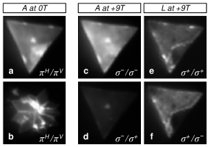
We return to polarimetric mapping to demonstrate that the main valleytronic signatures of layered TMDs discussed above can be obtained in direct two-dimensional imaging. To this end we defocussed the excitation laser to illuminate a spot of m diameter and replaced the single-mode fiber in the detection path with an imaging lens and a CCD. The resulting optical system images a sample area of m2 onto a single pixel of a standard room-temperature CCD array. A tunable band-pass filter placed before the CCD imaging lens was used to select exciton-specific bands, and polarimetric imaging was performed either in the circular or linear basis.
Polarimetric images of the two representatives flakes recorded in cross-linear configuration (orthogonal excitation and detection polarizations) within the exciton band are shown in Fig. 4a and b. In the given configuration, the high intensity features correspond to bilayer and dephasing regions of the flakes. Apart from a scaling factor, the images are equivalent to gray-scale versions of the false-color maps in Fig. 2e and f. They demonstrate qualitatively that disorder in monolayer TMDs can be visualized directly with a rather simple and efficient imaging technique. A quantitative analysis of the spatial distribution of can be carried out to yield maps analogous to Fig. 2c and d (see the Supplementary Information).
It is also straight forward to apply the technique in the circular basis. The images of Fig. 4c and d show the PL intensity of excitons in co-circular and cross-circular polarimetry for a magnetic field of T. The normalized difference of the images yields the profile equivalent to Fig. 3b (see the Supplementary Information). However, the non-thermalized exciton valley population of the upper Zeeman branch addressed by excitation can be readily deduced from Fig. 4c and d; for a fully thermalized valley population the flake in Fig. 4c would be less intense than in Fig. 4d. The analogous set of measurements for the exciton band in co- and cross-polarized configurations (Fig. 4e and f) illustrates the negative degree of circular polarization: the cross-polarized image of the flake is brighter (except for the puddle and a few hot-spots of point-like quantum dot emission) in accord with the raster-scan polarization image of Fig. 3c.
Conclusions
Our study identifies both raster-scan and wide-field polarimetric imaging as viable tools to explore the valley pseudospin physics in layered TMD semiconductors. Experiments that do not require the full spectral information but are meaningful within a limited PL bandwidth will benefit from a decrease of the measurement time required to achieve the same signal-to-noise performance in wide-field and hyperspectral raster-scan polarimetry. For m2 sample areas like in Fig. 4 we estimate a speed-up by at least three orders of magnitude for wide-field imaging as compared to raster-scanning (see the Supplementary Information) which enables rapid large-scale monitoring of the sample (see the Supplementary Video). Clearly, our polarimetric studies are not limited to MoS2 crystals but establish novel analytic means for the entire class of layered TMD semiconductors and heterostructures, and can be extended to spin-polarization imaging of conventional semiconductor quantum wells 21. It will perform most efficiently when applied on TMD materials with spectrally separated exciton and trion emission bands, a condition currently accessible with MoS2 only by chemical treatment 40. By virtue of simplicity and efficiency our technique will facilitate the analysis of TMD materials in terms of crystalline and environmental disorder and, combined with a microscopic model for the optical valley initialization, it will enable quantitative access to site-dependent valley pseudospin dynamics. Moreover, our findings encourage the experimental exploration of topological exciton-polaritons by identifying sufficiently large regions of low valley depolarization and decoherence in monolayer TMDs for the realization of periodic exciton potential arrays that are key to the implementation of topolaritonic devices 41.
References
- 1 Gunawan, O., De Poortere, E. P. & Shayegan, M. AlAs two-dimensional electrons in an antidot lattice: Electron pinball with elliptical Fermi contours. Phys. Rev. B 75, 081304 (2007).
- 2 Culcer, D., Saraiva, A. L., Koiller, B., Hu, X. & Das Sarma, S. Valley-based noise-resistant quantum computation using Si quantum dots. Phys. Rev. Lett. 108, 126804 (2012).
- 3 Rycerz, A., Tworzydło, J. & Beenakker, C. W. J. Valley filter and valley valve in graphene. Nat. Phys. 3, 172–175 (2007).
- 4 Xiao, D., Liu, G.-B., Feng, W., Xu, X. & Yao, W. Coupled spin and valley physics in monolayers of MoS2 and other group-VI dichalcogenides. Phys. Rev. Lett. 108, 196802 (2012).
- 5 Xu, X., Yao, W., Xiao, D. & Heinz, T. F. Spin and pseudospins in layered transition metal dichalcogenides. Nat. Phys. 10, 343–350 (2014).
- 6 Splendiani, A. et al. Emerging photoluminescence in monolayer MoS2. Nano Lett. 10, 1271–1275 (2010).
- 7 Mak, K. F., Lee, C., Hone, J., Shan, J. & Heinz, T. F. Atomically thin MoS2: A new direct-gap semiconductor. Phys. Rev. Lett. 105, 136805 (2010).
- 8 Kim, J. et al. Ultrafast generation of pseudo-magnetic field for valley excitons in WSe2 monolayers. Science 346, 1205–1208 (2014).
- 9 Cao, T. et al. Valley-selective circular dichroism of monolayer molybdenum disulphide. Nat. Commun. 3, 887 (2012).
- 10 Mak, K. F., He, K., Shan, J. & Heinz, T. F. Control of valley polarization in monolayer MoS2 by optical helicity. Nat. Nanotechnol. 7, 494–498 (2012).
- 11 Zeng, H., Dai, J., Yao, W., Xiao, D. & Cui, X. Valley polarization in MoS2 monolayers by optical pumping. Nat. Nanotechnol. 7, 490–493 (2012).
- 12 Zhang, Y. J., Oka, T., Suzuki, R., Ye, J. T. & Iwasa, Y. Electrically switchable chiral light-emitting transistor. Science 344, 725–728 (2014).
- 13 Mak, K. F., McGill, K. L., Park, J. & McEuen, P. L. The valley Hall effect in MoS2 transistors. Science 344, 1489–1492 (2014).
- 14 Sallen, G. et al. Robust optical emission polarization in MoS2 monolayers through selective valley excitation. Phys. Rev. B 86, 081301 (2012).
- 15 Lagarde, D. et al. Carrier and polarization dynamics in monolayer MoS2. Phys. Rev. Lett. 112, 047401 (2014).
- 16 Jones, A. M. et al. Optical generation of excitonic valley coherence in monolayer WSe2. Nat. Nanotechnol. 8, 634–638 (2013).
- 17 Wang, G. et al. Valley dynamics probed through charged and neutral exciton emission in monolayer WSe2. Phys. Rev. B 90, 075413 (2014).
- 18 Wu, S. et al. Electrical tuning of valley magnetic moment through symmetry control in bilayer MoS2. Nat. Phys. 9, 149–153 (2013).
- 19 Jones, A. M. et al. Spin-layer locking effects in optical orientation of exciton spin in bilayer WSe2. Nat. Phys. 10, 130–134 (2014).
- 20 Zhu, B., Zeng, H., Dai, J., Gong, Z. & Cui, X. Anomalously robust valley polarization and valley coherence in bilayer WS2. Proc. Natl. Acad. Sci. USA 111, 11606–11611 (2014).
- 21 Meier, F. & Zakharchenya, B. P. (eds.) Optical Orientation (Elsevier Science Publishers B.V., 1984).
- 22 Maialle, M. Z., de Andrada e Silva, E. A. & Sham, L. J. Exciton spin dynamics in quantum wells. Phys. Rev. B 47, 15776–15788 (1993).
- 23 Glazov, M. M. et al. Exciton fine structure and spin decoherence in monolayers of transition metal dichalcogenides. Phys. Rev. B 89, 201302 (2014).
- 24 Yu, T. & Wu, M. W. Valley depolarization due to intervalley and intravalley electron-hole exchange interactions in monolayer MoS2. Phys. Rev. B 89, 205303 (2014).
- 25 Tongay, S. et al. Defects activated photoluminescence in two-dimensional semiconductors: interplay between bound, charged, and free excitons. Sci. Rep. 3, 2657 (2013).
- 26 Van der Zande, A. M. et al. Grains and grain boundaries in highly crystalline monolayer molybdenum disulphide. Nat. Mater. 12, 554–561 (2013).
- 27 Najmaei, S. et al. Vapour phase growth and grain boundary structure of molybdenum disulphide atomic layers. Nat. Mater. 12, 754–759 (2013).
- 28 Srivastava, A. et al. Optically active quantum dots in monolayer WSe2. Nat. Nanotechnol. 10, 491–496 (2015).
- 29 He, Y.-M. et al. Single quantum emitters in monolayer semiconductors. Nat. Nanotechnol. 10, 497–502 (2015).
- 30 Koperski, M. et al. Single photon emitters in exfoliated WSe2 structures. Nat. Nanotechnol. 10, 503–506 (2015).
- 31 Chakraborty, C., Kinnischtzke, L., Goodfellow, K. M., Beams, R. & Vamivakas, A. N. Voltage-controlled quantum light from an atomically thin semiconductor. Nat. Nanotechnol. 10, 507–511 (2015).
- 32 Wang, G. et al. Giant enhancement of the optical second-harmonic emission of WSe2 monolayers by laser excitation at exciton resonances. Phys. Rev. Lett. 114, 097403 (2015).
- 33 Gong, Z. et al. Magnetoelectric effects and valley-controlled spin quantum gates in transition metal dichalcogenide bilayers. Nat. Commun. 4, 2053 (2013).
- 34 Li, Y. et al. Valley splitting and polarization by the Zeeman effect in monolayer MoSe2. Phys. Rev. Lett. 113, 266804 (2014).
- 35 Srivastava, A. et al. Valley Zeeman effect in elementary optical excitations of monolayer WSe2. Nat. Phys. 11, 141–147 (2015).
- 36 Aivazian, G. et al. Magnetic control of valley pseudospin in monolayer WSe2. Nat. Phys. 11, 148–152 (2015).
- 37 MacNeill, D. et al. Breaking of valley degeneracy by magnetic field in monolayer MoSe2. Phys. Rev. Lett. 114, 037401 (2015).
- 38 Wang, G. et al. Magneto-optics in transition metal diselenide monolayers. 2D Mater. 2, 034002 (2015).
- 39 Stier, A. V., McCreary, K. M., Jonker, B. T., Kono, J. & Crooker, S. A. Exciton diamagnetic shifts and valley Zeeman effects in monolayer WS2 and MoS2 to 65 Tesla. Nat. Commun. 7, 10643 (2016).
- 40 Cadiz, F. et al. Well separated trion and neutral excitons on superacid treated MoS2 monolayers. Appl. Phys. Lett. 108, 251106 (2016).
- 41 Karzig, T., Bardyn, C.-E., Lindner, N. H. & Refael, G. Topological polaritons. Phys. Rev. X 5, 031001 (2015).
Acknowledgments: We thank P. M. Ajayan for support in the establishment of materials synthesis conditions used in this study, P. Altpeter and R. Rath for assistance in the clean room, J. P. Kotthaus, B. Urbaszek and F. Wang for useful discussions, and P. Maletinsky and K. Karrai for valuable input on the manuscript. We gratefully acknowledge funding by the European Research Council under the ERC Grant Agreement no. 336749, the Volkswagen Foundation, the DFG Cluster of Excellence Nanosystems Initiative Munich (NIM), and financial support from the Center for NanoScience (CeNS) and LMUinnovativ.
Author contributions: A. N. and A. H. conceived the experiments. A. N. built the experimental setup. H. Y. organized the material aspect and prepared MoS2 flakes on SiO2/Si substrates with support from A. D. M.. S. N. and J. Lou provided inputs on growth parameters of MoS2 flakes at an initial stage of the project. A. N., M. N., and H. Y. performed basic characterization of the sample. A. N., J. Lin., and L. C. performed the measurements. A. N., J. Lin., L. C., and A. H. analyzed the data. A. N. and A. H. prepared the figures and wrote the manuscript. All authors commented on the manuscript.
Data availability statement: The data that support the plots within this paper and other findings of this study are available from the corresponding authors upon reasonable request.
Additional information: Supplementary information is available in the online version of the paper. Reprints and permission information is available online at www.nature.com/reprints. Correspondence and requests for materials should be addressed to H. Y. (hyamaguchi@lanl.gov) and A. H. (alexander.hoegele@lmu.de).
Methods: Monolayer MoS2 crystals on SiO2/Si substrates were prepared by means of CVD and subsequent transfer with polymethyl methacrylate (PMMA). Briefly, SiO2/Si substrates with MoO3 seeding particles were placed in a quartz furnace in the presence of sulfur powder. The furnace was heated to ∘C for min with a flow of inert gases (N2 and Ar) under atmospheric pressure. After cooling down to room temperature, MoS2 crystals were transferred onto p-doped SiO2/Si substrates with a conventional PMMA transfer method. The PMMA was removed by rinsing the sample with MoS2 on SiO2/Si in an acetone bath for three cycles of min.
Cryogenic confocal spectroscopy, raster-scan and wide-field imaging were performed in an ultra-low vibration closed-cycle cryostat (attocube systems, attoDRY1000) with a base temperature of K and a superconducting magnet with fields of up to T. The sample was positioned with nanopositioners (attocube systems, ANP101 series) into the focal plane of a low-temperature apochromat with a numerical aperture of (attocube systems, LT-APO/VIS/0.65) and confocal excitation and detection spots of m full-width at half-maximum diameters. Linear polarizers (Thorlabs, LPVIS and LPVISB), half- and quarter-waveplates (B. Halle, RAC 3 series) mounted on piezo-rotators (attocube systems, ANR240) were used to control the photon polarization in the excitation and detection pathways. PL spectroscopy was performed with continuous wave excitation lasers at nm (CNI, MLL-III-532-50-1) or nm (New Focus, Velocity TLB-6704), and a standard spectrometer (PI, Acton SP-2558) with a nitrogen cooled silicon CCD (PI, Spec-10:100BR/LN). The spectral resolution of the system was meV.
For wide-field polarimetric imaging, a femtosecond optical parametric oscillator operated at nm (Coherent, Mira-OPO) was defocussed to illuminate a sample area of mm2 at an average excitation power density of W/cm2. The PL was imaged with magnification onto a silicon CCD (Point Grey, GS3-U3-14S5M-C) within variable spectral bands set by tunable band-pass filters (Semrock, VersaChrome). The images of Fig. 4 were recorded with an encoding gamma of . The intensities were scaled to the full dynamic range of the grayscale by for Fig. 4a, c, and d, and for Fig. 4e and f, respectively. The image in Fig. 4b was not scaled.
SUPPLEMENTARY INFORMATION
Opto-valleytronic imaging of atomically thin semiconductors
Andre Neumann, Jessica Lindlau, Léo Colombier, Manuel Nutz,
Sina Najmaei, Jun Lou, Aditya D. Mohite, Hisato Yamaguchi, and Alexander Högele
1 Sample fabrication and basic characterization
The chemical vapor deposition (CVD) of monolayer MoS2 crystals was adopted from Najmaei and coworkers 1. Briefly, SiO2/Si substrates with MoO3 seeding particles were placed in a quartz furnace in the presence of sulfur powder. The furnace was heated to ∘C for min with a flow of inert gases (N2 and Ar) under atmospheric pressure. After cooling down to room temperature, synthesized MoS2 crystals were transferred onto p-doped SiO2/Si substrates with a conventional polymethyl methacrylate (PMMA) transfer method 2. The PMMA was removed by rinsing the resulting sample with MoS2 on SiO2/Si in an acetone bath for three cycles of min. Optical and atomic force microscopy (AFM) images of typical MoS2 monolayer flakes after transfer onto SiO2/Si are shown in Supplementary Fig. 1.
2 Experimental setup and settings
Cryogenic confocal spectroscopy, raster-scan and wide-field imaging were performed in an ultra-low vibration closed-cycle cryostat (attocube systems, attoDRY1000) with a base temperature of K and a superconducting magnet with fields of up to T. The sample was positioned with nanopositioners (attocube systems, ANP101 series) into the focal plane of a low-temperature apochromat with a numerical aperture of (attocube systems, LT-APO/VIS/0.65) and confocal excitation and detection spots with m full-width at half-maximum (FWHM) diameters. Linear polarizers (Thorlabs, LPVIS and LPVISB), half- and quarter-waveplates (B. Halle, RAC 3 series) mounted on piezo-rotators (attocube systems, ANR240) were used to control the photon polarization in the excitation and detection pathways. PL spectroscopy was performed with continuous wave (cw) excitation lasers at nm (CNI, MLL-III-532-50-1) or nm (New Focus, Velocity TLB-6704), and a standard spectrometer (PI, Acton SP-2558) with a liquid nitrogen cooled silicon CCD (PI, Spec-10:100BR/LN, gain setting of e-/count). The spectral resolution of the system was meV for confocal PL and cm-1 for Raman measurements. A streak camera (Hamamatsu, C5680-24S) and a femtosecond (fs) optical parametric oscillator (OPO) operated at nm or nm (Coherent, Mira-OPO) were used for time-resolved PL studies. The fiber-coupled system exhibited dispersion-limited temporal resolution down to ps depending on the spectral bandwidth and the length of the single-mode fiber. For wide-field imaging, the OPO was tuned to nm and defocussed to illuminate a sample area of mm2 at an average excitation power density of W/cm2. PL images with magnification were acquired in the spectral bands of tunable band-pass filters (Semrock, VersaChrome) with a silicon CCD (Point Grey, GS3-U3-14S5M-C, pixel size of m2 and saturation capacity of ke-). All wide-field images were recorded with an integration time of s ( s in Supplementary Fig. 10b) and a CCD gain setting of dB (except for dB in Fig. 4a of the main text and dB in Supplementary Fig. 10a - d). The images digitized to a bit format with bit conversion were acquired with linear gamma encoding (gamma encoding of in Fig. 4 of the main text). The intensities were multiplied with scaling factors ranging from to to span the full dynamic range of the grayscale (identical factors were used for co- and cross-polarized images of the same exciton bands).
3 Spectroscopy and polarimetry experiments
3.1 Basic spectral characteristics
The PL of monolayer MoS2 crystals on SiO2/Si was excited either non-resonantly at nm ( eV) or at nm ( eV) in resonance with the blue shoulder of the exciton. A non-resonant spectrum recorded on a regular position of the triangular flake is shown in Supplementary Fig. 2a (same as in Fig. 1b of the main text). The non-resonant PL exhibits contributions of both neutral and charged excitons, and due to unintentional doping of MoS2 crystals on p-doped SiO2/Si substrates 3. The asymmetric lineshape of the total PL (spectrum in Supplementary Fig. 2a) can be decomposed into two Lorentzians with equal FWHM linewidths of meV separated by the trion binding energy of meV 4. The near-resonant spectrum recorded with a long-pass filter at nm ( eV) in Supplementary Fig. 2b (gray and blue traces show for the same flake position non-resonant and near-resonant spectra, respectively) exhibited additional sharp features identified as Raman scattered photons by the substrate (Si) and the MoS2 monolayer, with assignments given in Supplementary Fig. 2c adopted from Ref. 5. The Raman spectra were useful to identify bilayer regions (as in the center of the single-crystal triangle) where they exhibited a characteristic splitting of the mode shown in Supplementary Fig. 2d under resonant excitation with the fundamental exciton 6. To avoid contamination of the opto-valleytronic properties of excitons by Raman photons, we selected a spectral band of meV width centered at eV near the PL maximum of the exciton emission and away from Raman resonances (the red spectral interval in Supplementary Fig. 2a - c is the same as in Fig. 1b of the main text ). Moreover, for the quantitative analysis of the degree of circular polarization of excitons presented in Fig. 3e of the main text, the contribution of was removed by fitting the total PL with two Lorentzians and subtracting the contribution of the trion PL from the spectral band chosen for the opto-valleytronic analysis as described above.
3.2 Time-resolved photoluminescence measurements
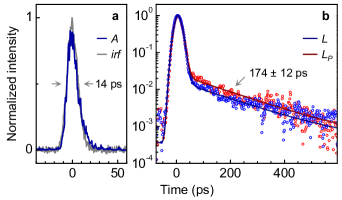
The PL decay dynamics of the monolayer MoS2 triangle from the main text are presented in Supplementary Fig. 3. The exciton PL, measured in a spectral band of meV, exhibited radiative decay with a time constant below the resolution limit of ps given by the dispersion-limited instrument response function (Supplementary Fig. 3a). Localized excitons, selected by a bandpass filter of meV width, exhibited two decay timescales (Supplementary Fig. 3b): the dominant fast component was resolution-limited (with partial contribution from excitons), and the slow component exhibited monoexponential decay with a lifetime of ps in agreement with previous results 7. The slow decay channel accounted for % of the total PL intensity on a regular position () and for % in the puddle () of the triangular crystal.
3.3 Spectral characteristics of polarization-resolved photoluminescence
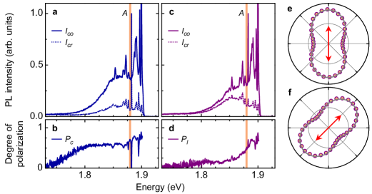
Supplementary Fig. 4a and c show co-polarized () and cross-polarized () PL spectra recorded with an excitation laser at nm ( eV) in circular and linear bases, respectively. The spectral characteristics of and , respectively shown in Supplementary Fig. 4b and d, were calculated as the normalized differences between co- and cross-polarized PL intensities according to . Data in Supplementary Fig. 4e and f confirm that the degree of linear polarization is independent of the choice of the linear basis (the linear PL polarization is parallel to the axis of the excitation laser set along and in Supplementary Fig. 4e and f, respectively). The red bar in Supplementary Fig. 4a - d was used for confocal opto-valleytronic imaging of excitons (same band as in Supplementary Fig. 2a - c and Fig. 1b of the main text).
3.4 Circular and linear raster-scan polarimetry
To construct polarimetric maps we raster-scanned the sample with respect to fixed confocal excitation and detection spots, and performed spectral acquisition of co- and cross-polarized PL at each raster pixel with an excitation power density of W/cm2. An averaged background spectrum was subtracted from all image pixels, and co- and cross-polarized PL intensities of and excitons were integrated within the spectral bands shown in Fig. 1b of the main text. Pixels with a standard deviation of above 0.05 (stemming from vanishingly small PL intensities away from the flake) were set to zero. In Supplementary Fig. 5a - d we reproduce the maps of Fig. 2a - d of the main text to indicate specific positions (numbered from to ) for a quantitative comparison of site-to-site variations of (blue bars) and (purple bars) summarized in Supplementary Fig. 5e for the of exciton band. Similar polarimetric measurements were performed on other MoS2 flakes. Supplementary Fig. 6a, c and Supplementary Fig. 6b, d show profiles of and for a poly-crystalline and a single-crystalline MoS2 monolayer, respectively. The bar chart in Supplementary Fig. 6e summarizes the statistics of and acquired on five different monolayer flakes.
3.5 Equivalence of polarization bases at zero magnetic field
In the absence of an external magnetic field, time-reversal symmetry implies the equivalence of the degrees of circular polarization measured in and configurations. The set of data in Supplementary Fig. 7a - c demonstrates that the degree of the circular polarization is independent of the choice of the circular basis: is identical (within the precision of our measurement) for and polarization bases (compare Supplementary Fig. 7a and b, respectively). This fact is also reflected by the vanishing difference profile shown in Supplementary Fig. 7c. The analogous set of data is respectively shown for the degrees of linear polarization recorded under horizontal () and diagonal () linearly polarized excitations in Supplementary Fig. 7d and e; their vanishing difference is plotted in Supplementary Fig. 7f. The data demonstrate the independence of of the choice of the linear basis.
3.6 Magnetic field dependence of the degree of circular polarization
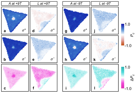
A finite external magnetic field applied in Faraday geometry (perpendicular to the TMD monolayer surface) lifts the valley degeneracy and gives rise to a Zeeman shift of opposite sign for excitons in the and valleys. A positive magnetic field decreases (increases) the energy of the () valley exciton. Consequently, an applied magnetic field changes the degrees of circular polarization of the valley exciton emission. The changes are discussed in the main text for spectrally selected and excitons under and excitation at T (the corresponding data of Fig. 3 are reproduced in Supplementary Fig. 8a, b, d, and e). In Supplementary Fig. 8c and f we plot for both types of excitons the change in the degree of circular polarization, quantified as . For excitons at T, is negative (magenta-colored) throughout the MoS2 flake (Supplementary Fig. 8c). This corresponds to a decrease (increase) of the () degree of circular polarization for the lower (upper) () Zeeman branch of excitons. The excitons show the same trend away from the puddle and reversed features in the puddle (cyan-colored region in Supplementary Fig. 8f) in accord with thermal population distribution discussed in the main text. The right panel of Supplementary Fig. 8 shows the same set of data but for T. The sign reversal of the magnetic field results in interchanged roles of and polarizations (Supplementary Fig. 8g, h, j, and k) and thus in a sign reversal of (Supplementary Fig. 8i and l).
3.7 Wide-field imaging and polarimetry
As described previously the confocal setup was modified for wide-field imaging by defocusing the excitation laser to illuminate a sample area of mm2 and by replacing the single-mode fiber in the detection path with an imaging lens and a silicon CCD. A tunable band-pass filter (with nm FWHM bandwidth) was inserted before the imaging lens to select exciton-specific bands. The corresponding setup schematics are shown in Supplementary Fig. 9a. A fs-OPO operated at nm was used to excite the PL at an average power density of W/cm2. This average power density was a factor of and lower than in confocal measurements with the excitation laser at nm (cw power density of W/cm2) and nm (cw power density of W/cm2), respectively. In the following, we discuss the main implications of the reduced power density for the observations in wide-field imaging and polarimetry.
To compare the confocal and wide-field imaging modes we recorded additional PL spectra and intensity maps in the confocal setup configuration at reduced power densities. In Supplementary Fig. 9b - g we present data recorded in the regime of low power excitation for the single-crystal MoS2 triangle discussed in the main text. A confocal PL spectrum recorded at an excitation power density comparable to that of the wide-field imaging mode is shown in Supplementary Fig. 9b. Colored bands indicate the spectral intervals that were used for the evaluation of confocal PL intensity maps in Supplementary Fig. 9f and g for and excitons, respectively. The bands were selected to match the setting of the band-pass filter in wide-field imaging.
At low excitation powers the PL intensity of excitons is not saturated (Supplementary Fig. 9c). This results in an increased intensity ratio of to exciton PL in the confocal spectrum of Supplementary Fig. 9b as compared to the data in Fig. 1b of the main text. Moreover, since the saturation responses of excitons away from the puddle and in the puddle are different (the respective data are denoted as and in Supplementary Fig. 9c), one expects a crossover in the relative PL intensities of defect-bound excitons in the puddle and on a regular position of the flake. This effect is observed in PL imaging at low excitation power densities: both wide-field (Supplementary Fig. 9e) and confocal (Supplementary Fig. 9g) images of the monolayer triangle show a more intense exciton PL away from the puddle, whereas at high excitation power densities the exciton PL in the puddle is more intense (Fig. 1e of the main text). The more pronounced appearance of hot-spots in the PL intensity profiles of excitons under low-power illumination (Supplementary Fig. 9d and f) as compared to the PL intensity map under high-power illumination (Fig. 1d of the main text) is also attributed to saturation effects.
As in confocal polarimetry, polarization-resolved wide-field imaging can be used to construct polarimetric profiles of valley polarization and valley coherence. To demonstrate the quantitative character of the technique, we show in Supplementary Fig. 10a - f the and profiles of the single-crystal MoS2 triangle of the main text obtained with wide-field polarimetry. Note that the opto-valleytronic profiles are in excellent quantitative agreement with confocal data shown in Fig. 2 and Fig. 3 of the main text if one takes into account the reduction of and due to wider spectral bands of the band-pass filter used in wide-field polarimetry.
The advantage of the wide-field imaging technique is that it reduces the integration time for opto-valleytronic profiling whenever full spectral information at each pixel of the map is not required. Ultimately, for an image size of m2 with a pixel size of m2 an acquisition acceleration of at least can be obtained with polarimetric profiling in wide-field imaging as compared to confocal raster-scanning with the same spatial resolution, spectral width, noise level, and transmission characteristics. For this estimation we neglected the confocal scanning time and assumed equal excitation power densities of the imaging techniques as well as shot-noise limited signals. We note that for our confocal raster-scan polarimetry the scanning time was a factor of two longer than the integration time, and the transmission properties were a factor of ten lower than for wide-field imaging.
4 Theoretical modeling
In the following we model the degree of circular polarization of excitons in monolayer MoS2 in the presence of an external magnetic field applied in Faraday geometry (the magnetic field is oriented perpendicular to the TMD monolayer surface). To this end we consider a four level system with the crystal ground state , the exciton state , the exciton state , and an excited state in one of the two valleys. All levels are denoted in Supplementary Fig. 11, where without loss of generality the excited state is in the valley. In the following, exciton states in () that couple to () polarized optical transitions are tagged with the valley index ().
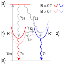
For a () polarized optical transition that is assumed to create population exclusively in the excited () state, the temporal evolution of the populations in each state is given by the following set of rate equations:
| (1) |
where is the population of the th state, is the temporal derivative of , and is the transition rate from state to . The population dynamics are governed by the following rates: denotes the absorption rate from the crystal ground state into an excited state in one of the two valleys, and are the valley conserving and valley flipping relaxation rates (or vice versa), and are the valley flipping rates among the and states, and is the and exciton decay rate (including both radiative and non-radiative channels). The total population of the system is normalized to , and steady-state solutions are obtained for .
The degree of circular polarization is obtained from steady-state populations and of the and valleys:
| (2) |
with the explicit expression equivalent to the one derived in the Supplementary Information of Ref. 8:
| (3) |
We rewrite this expression as:
| (4) |
with a branching parameter given by the ratio of the valley flipping to the valley conserving relaxation rates:
| (5) |
The definition of the branching parameter implies for ().
First, we examine the the degree of circular polarization given by Eqs. 3 and 4 at zero magnetic field. In the presence of time-reversal symmetry, the valley flipping processes are symmetric and thus . Moreover, in the limit of ideal initial polarization, i. e. for , Eqs. 3 and 4 simplify to:
| (6) |
where is the ratio of the zero-field longitudinal valley depolarization rate to the exciton decay rate . This expression is equivalent to the one derived in Ref. 9, and it corresponds to the steady-state degree of circular polarization in optical spin orientation with ideal initial polarization 10:
| (7) |
if we identify as the exciton lifetime and as the valley depolarization time. This limit where and thus are fixed by the degree of circular polarization was used in the main text to discuss the data at zero magnetic field.
If the initial polarization of the fundamental exciton populations in and valleys is non-ideal because of valley flipping events upon relaxation from the optically excited state, we have analogous to imperfect spin orientation 10:
| (8) |
with the initial polarization given by the yield of optical valley polarization of and populations at zero magnetic field in the presence of finite branching .
In a finite magnetic field applied perpendicular to the sample, the valley Zeeman splitting 11, 12, 8, 13, 14, 15 introduces an imbalance between and . In the presence of non-zero branching, we return to Eqs. 3 and 4 to recapitulate the findings of Ref. 8 with respect to the magnetic field evolution of . First we note qualitatively that due to the valley Zeeman splitting, the imbalance of and increases (decreases) the population transfer rate from the upper (lower) to the lower (upper) Zeeman branch. Thus, provided sufficiently rapid valley depolarization on the timescale of the exciton lifetime, we expect the population to relax into the energetically lower valley. Consequently, the of the upper (lower) Zeeman valley should decrease (increase) with magnetic field. The opposite trend is observed in our study of and excitons in monolayer MoS2 away from defects in agreement with the exciton response in monolayer WSe2 reported in Ref. 8. This counter-intuitive population distribution was attributed to (i) slow inter-valley scattering and (ii) polarization protecting branching ratio that decreases (increases) for the upper (lower) valley with magnetic field 8. Since no explicit expression for the functional form of the evolution of with magnetic field was given in Ref. 8, and to account for different materials and experimental conditions, we approximate with a linear function in :
| (9) |
where is the zero-field branching ratio and is a proportionality factor. It is worth noting that Eq. 9 should be interpreted as a low-field approximation since in it would yield unphysical negative values for in the limit of sufficiently high fields. Moreover, a difference in for the and valleys could account for broken time-reversal symmetry in absence of a magnetic field as pointed out in Ref. 8.
To proceed with the analysis of our data using the model of Ref. 8 where (or correspondingly ) was assumed, we fit the evolutions of the and excitons on a regular position of the triangular flake with , and as fitting parameters. The results of best fits to the data, obtained from least deviation (defined by the unweighted sum of squared deviations between fits and data and divided by the number of degrees of freedom), are presented in Supplementary Fig. 12.
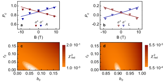
The non-thermal population distribution of both and excitons is reflected by the counter-intuitive -pattern of higher values for the Zeeman branches with higher energy. It is consistent with slow longitudinal valley depolarization on the timescale of the exciton lifetime, and best fits actually yield for both and excitons. The zero-field branching ratio for the selectively initialized population is small for excitons () and large for excitons () as expected from the less resonant excitation of the latter. In this framework, the evolution of the branching ratio with magnetic field critically determines the respective pattern: both and excitons exhibit an increasing protection of the optical valley polarization in the upper Zeeman valley as the branching ratio between the valley flipping and conserving relaxation rates decreases ( for both and ) due to exchange-modified exciton dispersions 8.
The model of Ref. 8 within the framework of Eqs. 4 and 9 requires vanishingly small values of without quantifying its smallness. To obtain an estimate for the ratio of the longitudinal valley depolarization time to the exciton lifetime, we extend the model of Ref. 8 by assigning thermal imbalances to the longitudinal inter-valley flipping rates and explicitly using the Boltzmann factor :
| (10) |
where, at a temperature , the exponent is determined by the Boltzmann constant and the valley Zeeman splitting linear in the magnetic field (with being the effective exciton -factor, and the Bohr magneton) 11, 12, 8, 13, 14, 15. The zero-field ratio , defined by the Eq. 6 above, is likely to exhibit a magnetic field dependence but short of knowledge of its functional form is assumed here as constant. The exponential imbalance of and is responsible for an effective unidirectional thermalization of population from the upper to the lower Zeeman branch during the exciton lifetime, and modifies Eq. 4 to:
| (11) |
The degree of circular polarization is now sensitive to the thermal imbalance of the inter-valley scattering rates through the Boltzmann factor, and it accounts for the non-zero branching in the polarization initialization with its characteristic magnetic field dependence via given by Eq. 9. The second term drives the thermal population distribution among the and valleys, while the first term counteracts this thermalization via the functional dependence of the branching ratio on the magnetic field in favor of a ’hot’ population distribution.
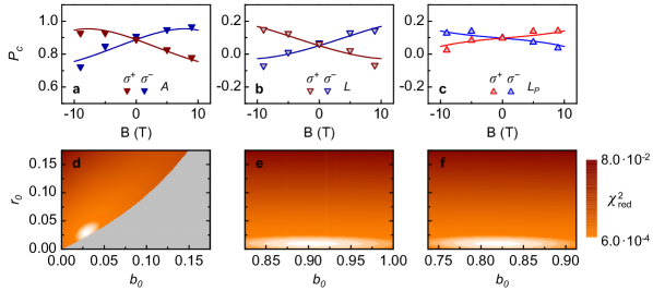
With this expression for the field-evolution of , we performed a simultaneous fit of our set of data for and excitons away from the puddle and excitons. To minimize the number of free fitting parameters, we assumed no field-dependence of for the case of excitons that exhibit a thermal population distribution, and set both the -factors and the ratios equal for both and . Moreover, we fixed the exciton -factor to 14, 15, and assumed a global temperature for the entire set of data. With these parameters fixed, best simultaneous fit was obtained with , , and for , , and ; for and for and ; T-1 for and T-1 for ; for and ; K. The corresponding evolutions of for , and excitons are shown in Supplementary Fig. 13a, b and c, respectively. We note that the best fit yielded an effective temperature of K consistent with local laser heating, and for and excitons in agreement with elevated values reported for excitons localized in quantum dots 16, 17, 18, 19.
The main effect of the model of Eq. 11 as compared to the model of Eq. 4 is the increased field dependence of the exciton branching ( increased by a factor of two from T-1 to T-1), whereas the values of the zero-field branching ratio of for the valley flipping to the valley conserving rate are comparable for the two models. Most importantly, the model yields an estimate for for both and localized excitons: bet fit values of for , and for and correspond to and , respectively. Taking the PL decay time of ps for the excitons in MoS2 7 that we do not resolve in our time-correlated PL experiments, we thus obtain an estimate for the longitudinal valley depolarization time of ps for excitons. With the same scaling we estimate ps for localized excitons that exhibit PL decay dynamics dominated by the fast component below the resolution limit of our fiber-based setup with dispersion (as shown in Supplementary Fig. 3b, only of the total PL intensity of both and excitons contribute to the slow decay component). The main difference for and populations stems from different branching during relaxation: while the upper valley polarization of excitons is weakly yet increasingly protected with magnetic field (with a slope of T-1), the branching ratio of excitons is independent of magnetic field. Given similar PL decay dynamics in the and bands, and similar branching ratios at zero magnetic field, we conclude that hot and thermal valley populations of localized excitons arise from field-dependent and field-independent branching ratios, respectively.
References
- 1 Najmaei, S. et al. Vapour phase growth and grain boundary structure of molybdenum disulphide atomic layers. Nat. Mater. 12, 754–759 (2013).
- 2 Reina, A. et al. Transferring and identification of single- and few-layer graphene on arbitrary substrates. J. Phys. Chem. C 112, 17741–17744 (2008).
- 3 Scheuschner, N. et al. Photoluminescence of freestanding single- and few-layer MoS2. Phys. Rev. B 89, 125406 (2014).
- 4 Berkelbach, T. C., Hybertsen, M. S. & Reichman, D. R. Theory of neutral and charged excitons in monolayer transition metal dichalcogenides. Phys. Rev. B 88, 045318 (2013).
- 5 Gołasa, K. et al. Multiphonon resonant Raman scattering in MoS2. Appl. Phys. Lett. 104, 092106 (2014).
- 6 Staiger, M. et al. Splitting of monolayer out-of-plane Raman mode in few-layer WS2. Phys. Rev. B 91, 195419 (2015).
- 7 Lagarde, D. et al. Carrier and polarization dynamics in monolayer MoS2. Phys. Rev. Lett. 112, 047401 (2014).
- 8 Aivazian, G. et al. Magnetic control of valley pseudospin in monolayer WSe2. Nat. Phys. 11, 148–152 (2015).
- 9 Mak, K. F., He, K., Shan, J. & Heinz, T. F. Control of valley polarization in monolayer MoS2 by optical helicity. Nat. Nanotechnol. 7, 494–498 (2012).
- 10 Meier, F. & Zakharchenya, B. P. (eds.) Optical Orientation (Elsevier Science Publishers B.V., 1984).
- 11 Li, Y. et al. Valley splitting and polarization by the Zeeman effect in monolayer MoSe2. Phys. Rev. Lett. 113, 266804 (2014).
- 12 Srivastava, A. et al. Valley Zeeman effect in elementary optical excitations of monolayer WSe2. Nat. Phys. 11, 141–147 (2015).
- 13 MacNeill, D. et al. Breaking of valley degeneracy by magnetic field in monolayer MoSe2. Phys. Rev. Lett. 114, 037401 (2015).
- 14 Wang, G. et al. Magneto-optics in transition metal diselenide monolayers. 2D Mater. 2, 034002 (2015).
- 15 Stier, A. V., McCreary, K. M., Jonker, B. T., Kono, J. & Crooker, S. A. Exciton diamagnetic shifts and valley Zeeman effects in monolayer WS2 and MoS2 to 65 Tesla. Nat. Commun. 7, 10643 (2016).
- 16 Srivastava, A. et al. Optically active quantum dots in monolayer WSe2. Nat. Nanotechnol. 10, 491–496 (2015).
- 17 He, Y.-M. et al. Single quantum emitters in monolayer semiconductors. Nat. Nanotechnol. 10, 497–502 (2015).
- 18 Koperski, M. et al. Single photon emitters in exfoliated WSe2 structures. Nat. Nanotechnol. 10, 503–506 (2015).
- 19 Chakraborty, C., Kinnischtzke, L., Goodfellow, K. M., Beams, R. & Vamivakas, A. N. Voltage-controlled quantum light from an atomically thin semiconductor. Nat. Nanotechnol. 10, 507–511 (2015).