One-dimensional edge contacts to a monolayer semiconductor
Abstract
Integration of electrical contacts into van der Waals (vdW) heterostructures is critical for realizing electronic and optoelectronic functionalities. However, to date no scalable methodology for gaining electrical access to buried monolayer two-dimensional (2D) semiconductors exists. Here we report viable edge contact formation to hexagonal boron nitride (hBN) encapsulated monolayer MoS2. By combining reactive ion etching, in-situ Ar+ sputtering and annealing, we achieve a relatively low edge contact resistance, high mobility (up to ) and high on-current density ( at = ), comparable to top contacts. Furthermore, the atomically smooth hBN environment also preserves the intrinsic MoS2 channel quality during fabrication, leading to a steep subthreshold swing of /dec with a negligible hysteresis. Hence, edge contacts are highly promising for large-scale practical implementation of encapsulated heterostructure devices, especially those involving air sensitive materials, and can be arbitrarily narrow, which opens the door to further shrinkage of 2D device footprint.
Two-dimensional electronic devices made from transition metal dichalcogenides (TMDCs) have gained prominence in recent years for next-generation integrated electronics Desai16 and nanophotonics applications. In particular, MoS2 combined with other 2D materials into vdW heterostructures, appears as an attractive candidate for future transistor architectures Iannaccone18 , atomically thin p-n junctions and tunnel diodes Frisenda2018b , memristors Wang2018b , high-efficiency photodetectors Bharadwaj15 , light emitting diodes Wang2018 and novel valleytronic devices Schaibley16 . Such heterostructures are often assembled in a top-down manner by picking-up discrete 2D material layers with a top hBN flake and placing the resulting stack on a target substrate. Although the presence of a top hBN layer on one hand serves to encapsulate the constituent 2D materials in the heterostructure, at the same time however, it also hinders the fabrication of direct electrical contacts to the underlying layers. Despite vdW heterostructures having been extensively investigated, a practical route for making electrical contacts to them in a scalable manner is still lacking.
In TMDC heterostructures assembled without any encapsulation layer, further limitations arise when electrical contacts are made in a conventional top-contact geometry. In this scenario, the contact electrodes come in direct physical contact with a TMDC layer over a finite area. Since such a methodology inherently requires performing lithography on unprotected TMDC layers, it exposes them to foreign chemical species which are difficult to remove. Additionally, bare TMDC surfaces in air are susceptible to O2 and H2O adsorption Qiu12 ; Jariwala13 ; Park13 . Owing to their atomically thin nature however, mono- and few-layer TMDCs are quite sensitive to their immediate environment which includes both surface adsorbates from ambient exposure and processing residues. These act as unintentional dopants leading to a spatially inhomogeneous carrier density Wu16 , which causes device-to-device variations in threshold voltage Rahimi16 ; Smithe2017b and Schottky barrier height Giannazzo15 . Besides doping, surface contaminants also scatter Ji2018 and trap charge carriers, thereby resulting in reduced mobility, low on-current Qiu12 ; Jariwala13 ; Park13 , increased flicker noise Sangwan13 ; Xie14 , hysteresis Shimazu16 and compromised optical properties Cho14 . Although measurements performed under high vacuum after in-situ annealing have made it possible to observe the intrinsic electrical transport properties of MoS2 Baugher13 ; Smithe2017a , unencapsulated devices measured in air show a drastic reduction in carrier mobility, implying that even short-term air exposure is detrimental for mono- and bi-layer MoS2 devices Qiu12 ; Jariwala13 .
Therefore, for enabling a viable usage of TMDCs in integrated electronics, better contact techniques are needed that allow for encapsulation before contact patterning, in order to preserve the intrinsic material quality and achieve superior performance. Moreover, encapsulation is also essential for long-term ambient stability since it is well-known that most TMDCs, including MoS2, MoSe2 and WS2 undergo gradual oxidation in air at room temperature Peto2018 , which leads to further mobility degradation Lee15 , morphological changes Park16 ; Gioele16 and adversely affected photoluminescence Gao16 . In fact, some 2D materials like MoTe2, HfSe2, ZrSe2, NbSe2, black phosphorus and InSe, are so unstable in air that surface deterioration can be detected within a day Gioele16 . This restricts their assembly to an inert atmosphere Cao15 and encapsulation in hBN is commonly employed to limit air exposure Cao15 ; Lee15 . With such materials, lithographic contact fabrication prior to encapsulation is not only difficult but also impractical.
In order to circumvent the issue of making electrical contacts to hBN-TMDC-hBN heterostructures, a common practice is to embed additional layers of graphene Lee15 ; Cui15 ; Liu2015a or metallic NbSe2 Guan17 ; Sata17 within the stack to act as electrodes. Pre-patterning contact vias into the top hBN before pick-up Wang15b ; Telford18 or transfer of pre-patterned metal films onto TMDCs Liu2018 (or vice-versa) have also been reported. However, alignment and transfer of multiple contact layers severely increases the fabrication complexity, especially in multilayer heterostructures, and becomes difficult to scale-up for practical purposes. Moreover, in case of graphene, the contact resistance () sensitively depends on the twist angle between the graphene and TMDC layers which poses further alignment challenges Liao2018 . Even though large-area chemical vapor deposition (CVD) growth of lateral graphene-MoS2 heterostructures has made progress in recent years Ling16 ; Guimaraes16 ; Zhao16 , hard to control growth inhomogeneities Zhao16 ; Suenaga2018 as well as ripples and strain induced by lattice mismatch still exist along 2D-2D edge interfaces Han2018 , which could ultimately hinder fabrication of very short channel () devices. Another possibility is to fabricate tunneling contacts on encapsulated TMDCs Wang16 ; Cui17 ; Li17 ; Ghiasi2018 . However, such devices are restricted to very thin hBN (1-4L) or oxide () Lee2016 encapsulation layers for optimum carrier injection. A more versatile approach is to etch through the top hBN layer in order to expose an edge of any buried 2D material of interest and form a one-dimensional (1D) ‘edge contact’ to it Wang13 ; Karpiak2017 . Although such a strategy has been highly successful for graphene Wang13 , similar attempts to make 1D edge contacts to monolayer (1L) MoS2 Chai16 ; Moon17 and few-layer WSe2 Xu16 were met with limited success until now.
Here we report reliable edge contact formation to hBN encapsulated 1L-MoS2. Our devices exhibit very low hysteresis together with a high mobility and steep subthreshold swing, highlighting the pristine interface quality achieved. By a systematic optimization of the fabrication process, we obtain a moderately low contact resistance and a high on-current () with Ti-Au edge contacts, despite a vanishingly small contact area. The contact performance remains unchanged even at low temperatures, making edge contacts promising for cryogenic experiments and applications. Thus, our work introduces a universal approach for making efficient contacts to encapsulated 2D semiconductors, especially those sensitive to air, and marks an important step towards pristine devices with homogeneous electrical and optical characteristics on a macroscopic scale. We believe that with further improvement of the edge contact interface, by minimizing disorder and passivating in-gap edge states, as discussed later, even smaller is achievable.
Edge contacts fabrication
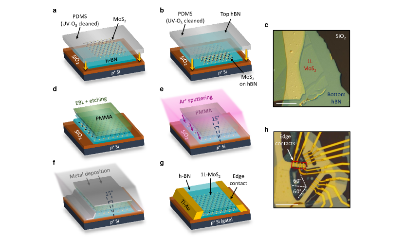
We will now discuss the fabrication strategy that we developed. Detailed process parameters can be found in Supporting Section S1. Bottom hBN flakes were exfoliated directly on p+Si/SiO2 () substrates. 1L-MoS2 and top hBN flakes were separately exfoliated on GelPak® PDMS (poly-dimethylsiloxane) stamps and transferred sequentially onto a suitable bottom hBN flake, as illustrated schematically in Figs. 1a, b. We found that PDMS can leave substantial residues behind after transfer which we minimized by pre-cleaning the PDMS surface in ultraviolet-ozone (UV-O3) prior to exfoliation (see Ref. Jain2018, for details). After each transfer, the resulting stack was annealed at in high-vacuum for to release trapped bubbles, wrinkles and strain (if any) induced by PDMS during transfer Jain2018 . Figure 1c shows the optical image of a 1L-MoS2 flake transferred onto hBN from PDMS. To fully encapsulate the MoS2, another hBN flake was subsequently transferred on top.
For device fabrication, bubble-free areas were chosen and patterned into rectangular sections by e-beam lithography (EBL) with PMMA (poly-methylmethacrylate) and reactive ion etching (RIE). Contact trenches were defined in a second EBL step and the exposed hBN-MoS2-hBN was etched away by RIE to create MoS2 edges for making contacts, as depicted in Fig. 1d (also see Supporting Fig. S1). The samples were then loaded into an e-beam evaporator for metal deposition, which we found to be the most critical part of the whole fabrication process. An etched MoS2 edge consists of dangling bonds as well as defects like Mo- and S-vacancies that are much more reactive than the basal plane of MoS2 Martincova2017 . During the time elapsed between etching and metal deposition, O2 and H2O molecules can not only bind to such edge sites but also potentially convert unpassivated Mo into MoOx Martincova2017 . However, MoOx, which is often used as a hole transport layer in solar cells, hinders electron injection into MoS2 due to its high work-function Santosh2016 . This scenario is in strong contrast to top contacts where MoOx formation is unlikely.
Hence, immediately before metal deposition, MoOx and any adsorbed O2 or H2O were removed by in-situ Ar+ sputtering at 15° tilt angle to expose a fresh MoS2 edge (Fig. 1e). Tilting the sample is necessary to access the etched hBN-MoS2-hBN sidewalls shadowed by an overhanging PMMA bilayer with an inward slope and avoid re-deposition of sputtered PMMA over the MoS2 edges. Ti-Au (5-) was then deposited at 15° tilt under a base pressure of (Fig. 1f-g). After lift-off, the devices were annealed in Ar H2 at for 3 hrs to improve the Ti-MoS2 edge interface and reduce contact resistance (Supporting Section S2). Note that the use of Ti is essential for providing good adhesion to hBN sidewalls. Without Ti, pure Au tends to reflow and lose contact during annealing at (Supporting Section S4). The final set of devices with edge contacts are shown in Fig. 1h.
Electrical characterization
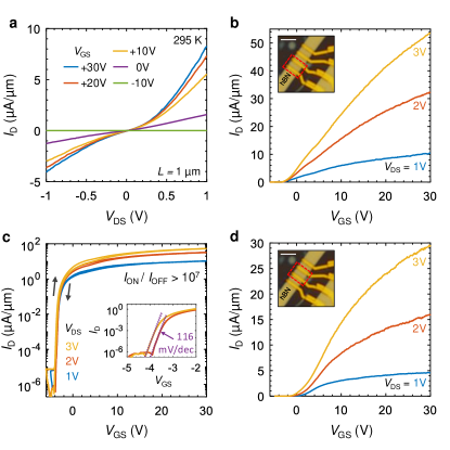
Figure 2a shows the - output characteristics of an edge contacted 1L-MoS2 transistor exhibiting n-type behavior. A slight non-linearity at low indicates the presence of a small barrier at the contacts, as predicted by our quantum transport simulations (Supporting Section S6) and other computational studies Guo2015 ; Dong2019 . The - transfer characteristics of the same device are plotted in Figs. 2b-c on linear and log scales, respectively. A high current density reaching at = with an on-off ratio can be observed. This clearly demonstrates that an efficient carrier injection is achievable via edge contacts, despite the lack of a 2D overlap between MoS2 and Ti. In Fig. 2c, each curve is comprised of both forward and backward sweeps which display a very small hysteresis. A magnified plot of the subthreshold characteristics is shown in the inset of Fig. 2c and reveals a low subthreshold swing (SS) of /dec maintained up to nearly 4 orders of magnitude. Realization of such a steep slope and low hysteresis was made possible here by encapsulation in hBN which not only protects the MoS2 channel from processing residues, but also provides an atomically smooth dielectric interface free of dangling bonds and defects. This significantly decreases the interface trap density in comparison with an exposed MoS2 layer on a SiO2 substrate. Moreover, the absence of thermally populated surface optical phonons in hBN at room temperature leads to a reduced scattering rate and enhanced carrier mobilities in MoS2 Dean10 . Using the relation Sze2006 ,
| (1) |
where is the gate capacitance per unit area and is the interface capacitance per unit area, we estimated the density of interface trap states = . This value is at least an order of magnitude lower than for unencapsulated, lithographically exposed MoS2 on SiO2 Zou2014 ; Choi2015 and ZrO2 Desai16 . Note that in this sample, the SS is primarily limited by the back-gate dielectric thickness ( SiO2 hBN). From Eq. (1), it is evident that for a larger gate capacitance (thinner dielectric), a smaller SS approaching the room temperature thermionic limit of /dec is anticipated. The - characteristics of a second device on the same sample are plotted in Fig. 2d, displaying a current density comparable to Fig. 2b.
To investigate the influence of the metal-MoS2 contact edge cleanliness on carrier injection, a set of three control devices that were not Ar+ sputtered, were also fabricated on the same hBN-MoS2-hBN stack shown in Fig. 1h (outlined in red). All control devices conduct a significantly lower than in Figs. 2b-d, indicating that carrier injection can be hindered if the MoS2 edge is not freshly cleaned immediately before metal deposition (Supporting Section S5). Additionally, it has been reported that Ti can partially oxidize during evaporation, depending on the vacuum level inside the deposition chamber, and thereby result in TiOx formation at the contact interface McDonnell16 . To inhibit the oxidation of Ti, we deposited Ti-Au on another set of devices (again without Ar+ sputtering) at a 10x lower base pressure of , with negligible residual O2 (Supporting Section S5). However, a low is also observed in this case, revealing the existence of an dominated transport. This implies that a better vacuum does not lead to any appreciable change in the contact properties if Ar+ sputtering is not done. It must be emphasized that an optimum post-deposition annealing temperature is also crucial for improving the contact interface (Supporting Section S2). Hence, our key finding here is that a clean MoS2 edge (before metallization) and annealing (after metallization) are both essential for forming good edge contacts, like those demonstrated in Figs. 2b-d. This likely explains why such a high current density had not been observed previously Chai16 ; Moon17 .
Next, we want to characterize the intrinsic carrier mobility () and contact resistance () of our devices. For an ideal long-channel nMOSFET operating in the strong inversion regime, a linear dependence of on is expected, given by
| (2) |
where is the threshold voltage and the internal drain () and gate () voltages are equal to the externally applied bias. Typically, is extracted from the slope of linear - characteristics with the help of Eq. (2). However, Fig. 2b shows that grows sub-linearly with for all , which causes the mobility extracted in this manner to be underestimated. For a more accurate description of such - behavior, the presence of finite contact resistances in series with the MoS2 channel must be considered. In this scenario, the internal voltages seen by the channel get reduced to and . Note that also gets modified to but the drain-induced barrier lowering (DIBL) factor is small enough to be neglected in our long-channel devices. Equation (2) can then be re-written as
| (3) |
Rearranging Eq. (3) to solve for , we obtain
| (4) | |||
From Eq. (4), we can infer that when , increases sub-linearly with . To exclude the effect of , one can first calculate , as shown by Ghibaudo Ghibaudo1988 and Jain Jain1988 , where is the transconductance of the device.
| (5) |
Upon multiplying Eqs. (4) and (5), can be eliminated and an expression commonly known as the -function is obtained, which depends linearly on .
| (6) |
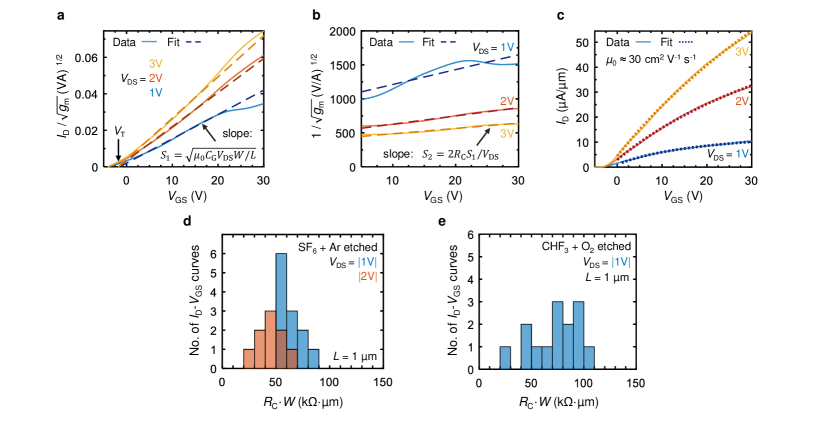
By plotting vs. and using Eq. (6), the mobility () and threshold voltage () can be extracted from the slope () and x-intercept, respectively Smithe2017b ; Chang2014 . Figure 3a is a plot of the -function for the data in Fig. 2b. It shows an approximately linear behaviour in the strong inversion regime from which a value of = can be derived. Lastly, we plot vs. (Fig. 3b) and extract the slope () of the linear region. can then be determined from the relation , derived using Eqs. (4)–(6) Cho2018 . However, we found that due to random undulations of the derivative , the plots in Fig. 3b do not always remain linear in the entire range for every device. As a consequence, the extracted slope can vary depending on the range chosen for the 1D polynomial fit. Hence, for a more reliable estimation of device parameters, we followed a slightly different approach and directly fitted our - curves with Eq. (4), choosing all three unknowns (, and ) as fitting parameters. We found this procedure to be more straightforward than the commonly used -function method.
Figure 3c is a reproduction of the plots in Fig. 2b, fitted with Eq. (4) in the inversion regime for each . The excellent quality of the fits indicates that the model in Eq. (4) describes our - characteristics very well. The estimated mobility = is also in good agreement with the value obtained from the -function plots in Fig. 3a. Knowing and from the fits, the contact resistance could then be deduced using Eq. (4) to be = 27.8, 11.7 and µm at = 1, 2 and , respectively. It was found to decrease with increasing owing to enhanced Schottky barrier tunneling at higher bias voltages, as indicated by the non-linear - characteristics in Fig. 2a. Interestingly, these numbers are very similar to room temperature values reported for graphene top contacts on hBN encapsulated 1L-MoS2 devices (µm) Cui15 as well as CVD grown lateral graphene - MoS2 contacts (10-µm) Guimaraes16 ; Zhao16 . But at the same time, compared to the latter case, we observe a higher mobility owing to hBN encapsulation. These results unambiguously demonstrate that edge contacts can replace graphene contacts in encapsulated devices and achieve better performance with a less restrictive and scalable fabrication methodology. Moreover, use of graphene with MoS2 is currently limited to electron injection only, whereas with a proper choice of edge contact material, hole injection can also be feasible Guo2015 .
For completeness, it should be clarified that in our analysis is assumed to be independent of whereas in conventional contacts, it decreases asymptotically with increasing carrier density for low near the onset of inversion, and slowly saturates at high . Such a behavior arises from the fact that in Ti-MoS2 top contacts with an interfacial oxide (often unintentional), increasing reduces the sheet resistivity of MoS2 below the contact region and also lowers the potential barrier for electron injection into MoS2 Szabo2019 , which increases the effective current transfer length Liu2014c . Moreover, at the same time the applied also pushes the conduction band (CB) minimum closer to the metal Fermi level, thereby bending the CB more steeply near the contact edge, which narrows the effective Schottky barrier width Liu2014c . This two-fold mechanism leads to a strong reduction of in top contacts as increases Allain2015 . However, in edge contacts where a 2D metal-MoS2 overlap region is absent (), the primary mechanism behind reduction with increasing is Schottky barrier narrowing, being more pronounced near the subthreshold region and saturating soon after. This causes to show a gate dependence that is weak enough to be neglected for , as substantiated by the constant slopes and in Figs. 3a-b for , which justifies our initial assumption. The model in Eq. (4) also fits well only in this regime. Hence, the we estimated is the independent value at large carrier densities, similar to Ref. Chang2014, . The most accurate way of extracting is the transfer length method (TLM). However, it requires fabrication of several devices with decreasing channel lengths and only works well when all devices have a very similar and , such that a plot of total resistance vs. channel length follows a straight line. This has turned out to be challenging at present for our devices. Hence, we employed a simpler method, which gives a reasonable estimate of and for every single device and also helps in quantifying the device-to-device variability, unlike TLM.
Besides the device in Fig. 3c, we obtained similarly good fits for - curves measured from additional devices, which further corroborates the model we used (see Supporting Section S3 for more - datasets). From these fits, an average = (20.5 5.5) was found, where the error margin represents one standard deviation. To study the influence of etched hBN sidewall profiles on edge contacts, we tested two different hBN etch recipes Wang13 ; Autore2018 . Figures 3d-e are histograms of extracted from devices etched using the two recipes. For SF6 Ar etched devices, we estimate an average = (64.2 9.6) µm at = (blue bars). Since our - curves are slightly asymmetric in general (Fig. 2a), we extracted values from - fits for both positive and negative . Some devices were also measured at = (orange bars) with an average = (46 10) µm. In contrast to SF6 Ar etched devices, those etched with CHF3 O2 show a wider distribution (Fig. 3e) and a higher mean value of = (73.5 23.4) µm. We attribute this increased variability to greater etching inhomogeneity resulting from CHF3 O2 in comparison with SF6 Ar, which we discovered upon scanning electron microscopy of bare hBN sidewalls (Supporting Fig. S1).
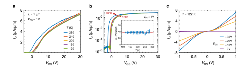
We further characterized another edge contacted 1L-MoS2 device at low temperatures inside a liquid nitrogen filled cryostat and is presented in Fig. 4. Apart from the expected shift in threshold voltage to higher values Sze2006 , we find that the - characteristics as well as the edge contact resistance in Figs. 4a-b remain essentially unchanged up to . This observed temperature insensitivity of agrees very well with previous findings on 1D edge contacts to graphene Wang13 as well as CVD grown graphene edge contacts to 1L-MoS2 Guimaraes16 , and demonstrates that carrier injection into MoS2 via edge contacts occurs efficiently even under cryogenic conditions. Moreover, the - characteristics at plotted in Fig. 4c, behave similar to those at room temperature seen earlier for the device in Fig. 2a. To shed some light on this behavior, we performed ab initio quantum transport simulations following the procedure described in our earlier publication Szabo2019 and are discussed in Supporting Section S6. In brief, the majority of the current injected via Ti edge contacts into MoS2 does not come from thermionic emission over the contact Schottky barrier, but rather tunneling across the barrier. Since the electron transmission probability near the Fermi level remains relatively constant as a function of energy (Supporting Fig. S10), the tunneling current varies only weakly with temperature. We found that this tendency persists for a range of Schottky barrier heights that were evaluated.
Discussion and conclusions
Strictly speaking, the true bandstructure of a semiconductor is defined for a lattice with an infinitely repeating unit cell. At MoS2 edges and grain boundaries, dangling bonds and Mo-, S-vacancies perturb the MoS2 bandstructure and give birth to additional localized ‘edge states’ within the bandgap, as measured experimentally Bollinger2001 ; Wu16 . Such states were also observed in air-exposed MoS2 Wu16 and WSe2 Addou2018 devices, implying that adsorbed O2 and H2O do not fully passivate them. Passivation of dangling bonds and edge states is essential for good edge contacts Houssa2019 , which may be achieved by Ti-MoS2 bonding. However, if a van der Waals gap or trapped air molecules are present between the MoS2 edge and Ti, edge state passivation could be hindered, resulting in a high density of in-gap states at each electron injection site. By trapping incoming electrons, these states can cause a space charge region to build up which would repel further injected electrons. In this regard, in-situ Ar+ sputtering plays a key role in producing a clean MoS2 edge immediately before Ti deposition. Subsequent annealing at promotes atomic rearrangement and Ti-MoS2 bonding. The need for such extra measures does not arise in the case of edge contacts to graphene, where edge states (if any) are unable to trap carriers because of the absence of a bandgap. Even O2 incorporation at the graphene edge was shown to have a negligible effect Wang13 , thus greatly simplifying fabrication of edge contacts to graphene. This scenario is fundamentally different from top contacts where the injected electrons do not encounter any edge states since the translational symmetry of the underlying MoS2 lattice is not broken (in the absence of interfacial reactions and defects) and on the contrary, a vdW gap is beneficial for avoiding Fermi level pinning Liu2018 .
Interactions between the contact metal and MoS2 at the atomic scale and structural characteristics of the contact interface play a significant role in governing the performance of any contact. For edge contacts in particular, where carrier transfer is restricted to a single atomic edge, an optimum metal-MoS2 interface is crucial. This makes them more challenging to fabricate compared to top contacts which impose fewer constraints and can tolerate local non-idealities to a greater extent due to the availability of a finite area. Our main achievement here lies in the development of an optimized process for realizing low resistance edge contacts with a high density of current injection per atomic site. Further studies are needed nevertheless to unravel the rich physics and chemistry occurring at the contact interface. Atomically resolved cross-sectional transmission electron microscope (TEM) imaging can be performed to gain better insights into the contact morphology, interface quality and atomic configuration of edge contacts. This would lead to a deeper understanding of the transport behavior and provide valuable guidelines for further improvement of the contact performance. It is possible that unpassivated edge states at interface voids still undermine the performance of our devices Houssa2019 and also cause undesired Fermi level pinning Chen2017 . Suitable chemical termination of dangling bonds could be a promising strategy to passivate edge states, de-pin the metal Fermi level and reduce even further. Apart from MoS2, air sensitive TMDCs like HfS2, ZrS2, etc. where edge states are expected to lie at shallow levels close to the band extrema, which makes them more immune to defects, appear as attractive materials for edge contacts Pandey2016 .
It should be emphasized that even though long Ti-Au Liu2015b , Ag-Au Smithe2017b and In-Au Wang2019 top contacts on 1L-MoS2 have resulted in a lower than that obtained in this work, in order to be fair, a comparison should be made with top contacts scaled down to sub-nm overlap lengths. However, it has been shown that the begins to increase considerably for contact lengths smaller than the current transfer length in both mono-Liu2014c and multi-layer MoS2 English2016 . This implies that conventional contacts cannot be scaled down beyond a certain limit, thereby restricting the minimum achievable device footprint (gate length + 2 x contact length). To ensure scaling of TMDC based devices, scalable contact geometries that work efficiently irrespective of dimensions are necessary. This bottleneck could be overcome by means of edge contacts, which do not require a 2D overlap with TMDCs and thus, in principle, can be made as narrow as possible. Another domain where edge contacts can outperform top contacts is multilayer TMDCs, in which carrier injection only via the topmost layer suffers from added interlayer hopping resistances that limit the current transport to top few layers Das2013 , whereas with edge contacts, each layer can be individually contacted for achieving higher current densities Schulman2018 . In this regard, 1T-phase edge contacts to few layer MoS2 Kappera2014 and MoTe2 Sung2017 also seem to be an attractive choice, although inducing a 2H 1T phase transition under the contact regions after encapsulation can be problematic.
Lastly, the possibility to encapsulate 2D materials before processing with chemicals remains the biggest advantage of edge contacts for building clean devices. Fundamental studies rely on high interface quality and macroscopic homogeneity for uncovering new physical phenomena, which can benefit from edge contacts fabricated after encapsulation. Edge contacts are especially promising for 2D materials unstable in air for which fabrication of top contacts is challenging due to restrictions imposed by encapsulation inside an inert atmosphere before being exposed to air. Often such heterostructures are built in a top-down manner and the need to make contacts to buried layers demands pick-up of additional graphene sheets. In such scenarios, edge contacts provide a much higher flexibility in heterostructure assembly and can be scaled-up to integrated circuits employing multiple metal layers separated by insulating dielectric layers. Thus, we envision that edge contacts will bring devices based on 2D materials one step closer to practical implementation and open up new pathways in 2D materials research.
Associated Content
Supporting Information. Detailed description of the fabrication procedure, plots showing the influence of annealing, data from additional devices, pure Au edge contacts without Ti, edge contacts without Ar+ sputtering, quantum transport simulations.
Methods
Edge contact fabrication. See Supporting Section S1 for a step-by-step process flow.
Electrical characterization. I-V measurements were carried out using a Keithley 2602B source meter in two-probe configuration. All devices were measured in air at room temperature (except those shown in Fig. 4). For calculating , the - curves were smoothened by cubic spline interpolation in MATLAB to reduce the noise before differentiation.
Acknowledgments
This research was supported by the Swiss National Science Foundation (grant no. 200021_165841), ETH Zürich (ETH-32 15-1) and CSCS (Project s876). Use of the cleanroom facilities at the FIRST Center for Micro and Nanoscience, ETH Zürich is gratefully acknowledged. TT and KW acknowledge support from the Elemental Strategy Initiative conducted by the MEXT, Japan and JSPS KAKENHI (grant no. JP15K21722). AJ would like to thank Aroosa Ijaz for invaluable help during sample fabrication.
Author Contributions
ML, AJ and LN conceived the project. AJ developed the fabrication procedure, carried out the measurements and analyzed the experimental data. ÁS and ML performed the quantum transport simulations. MP built the electrical characterization setup, wrote the LabVIEW scripts for recording I-V data and provided experimental support at various stages. Low temperature transport measurements were performed together with EB. TT and KW synthesized the hBN crystals used in this study. LN, ML and PB supervised the project. AJ wrote the manuscript with inputs from MP, ML and LN.
References
- (1) Desai, S. B. et al. MoS2 transistors with 1-nanometer gate lengths. Science 354, 99–103 (2016).
- (2) Iannaccone, G., Bonaccorso, F., Colombo, L. & Fiori, G. Quantum engineering of transistors based on 2D materials heterostructures. Nature Nanotech. 13, 183–191 (2018).
- (3) Frisenda, R., Molina-Mendoza, A. J., Mueller, T., Castellanos-Gomez, A. & van der Zant, H. S. J. Atomically thin p–n junctions based on two-dimensional materials. Chem. Soc. Rev. 47, 3339–3358 (2018).
- (4) Wang, M. et al. Robust memristors based on layered two-dimensional materials. Nature Electron. 1, 130–136 (2018).
- (5) Bharadwaj, P. & Novotny, L. Optoelectronics in flatland. Optics and Photonics News 26, 24–31 (2015).
- (6) Wang, J., Verzhbitskiy, I. & Eda, G. Electroluminescent devices based on 2D semiconducting transition metal dichalcogenides. Adv. Mater. 30, 1802687 (2018).
- (7) Schaibley, J. R. et al. Valleytronics in 2D materials. Nat. Rev. Mater. 1, 16055 (2016).
- (8) Qiu, H. et al. Electrical characterization of back-gated bi-layer MoS2 field-effect transistors and the effect of ambient on their performances. Appl. Phys. Lett. 100, 98–101 (2012).
- (9) Jariwala, D. et al. Band-like transport in high mobility unencapsulated single-layer MoS2 transistors. Appl. Phys. Lett. 102, 4–8 (2013).
- (10) Park, W. et al. Oxygen environmental and passivation effects on molybdenum disulfide field effect transistors. Nanotechnology 24, 095202 (2013).
- (11) Wu, D. et al. Uncovering edge states and electrical inhomogeneity in MoS2 field-effect transistors. Proc. Natl. Acad. Sci. USA 113, 8583–8588 (2016).
- (12) Rahimi, S. et al. The positive effects of hydrophobic fluoropolymers on the electrical properties of MoS2 transistors. Appl. Sci. 6, 236 (2016).
- (13) Smithe, K. K. H., Suryavanshi, S. V., Muñoz Rojo, M., Tedjarati, A. D. & Pop, E. Low variability in synthetic monolayer MoS2 devices. ACS Nano 11, 8456–8463 (2017).
- (14) Giannazzo, F., Fisichella, G., Piazza, A., Agnello, S. & Roccaforte, F. Nanoscale inhomogeneity of the Schottky barrier and resistivity in MoS2 multilayers. Phys. Rev. B 92, 081307 (2015).
- (15) Ji, H. et al. Gas adsorbates are coulomb scatterers, rather than neutral ones, in a monolayer MoS2 field effect transistor. Nanoscale 10, 10856–10862 (2018).
- (16) Sangwan, V. K. et al. Low-frequency electronic noise in single-layer MoS2 transistors. Nano Letters 13, 4351–4355 (2013).
- (17) Xie, X. et al. Low-frequency noise in bilayer MoS2 transistor. ACS Nano 8, 5633–5640 (2014).
- (18) Shimazu, Y., Tashiro, M., Sonobe, S. & Takahashi, M. Environmental effects on hysteresis of transfer characteristics in molybdenum disulfide field-effect transistors. Sci. Rep. 6, 6–11 (2016).
- (19) Cho, K. et al. Gate-bias stress-dependent photoconductive characteristics of multi-layer MoS2 field-effect transistors. Nanotechnology 25, 155201 (2014).
- (20) Baugher, B., Churchill, H. O. H., Yang, Y. & Jarillo-Herrero, P. Intrinsic electronic transport properties of high quality monolayer and bilayer MoS2. Nano Lett. 13, 4212–4216 (2013).
- (21) Smithe, K. K., English, C. D., Suryavanshi, S. V. & Pop, E. Intrinsic electrical transport and performance projections of synthetic monolayer MoS2 devices. 2D Materials 4, 1–8 (2017).
- (22) Peto, J. et al. Spontaneous doping of the basal plane of MoS2 single layers through oxygen substitution under ambient conditions. Nature Chem. 10, 1246–1251 (2018).
- (23) Lee, G.-H. et al. Highly stable, dual-gated MoS2 transistors encapsulated by hexagonal boron nitride with gate-controllable contact resistance and threshold voltage. ACS Nano 9, 7019–7026 (2015).
- (24) Park, J. H. et al. Scanning tunneling microscopy and spectroscopy of air exposure effects on molecular beam epitaxy grown WSe2 monolayers and bilayers. ACS Nano 10, 4258–4267 (2016).
- (25) Mirabelli, G. et al. Air sensitivity of MoS2, MoSe2, MoTe2, HfS2, and HfSe2. J. Appl. Phys. 120, 125102 (2016).
- (26) Gao, J. et al. Aging of transition metal dichalcogenide monolayers. ACS Nano 10, 2628–2635 (2016).
- (27) Cao, Y. et al. Quality heterostructures from two-dimensional crystals unstable in air by their assembly in inert atmosphere. Nano Lett. 15, 4914–4921 (2015).
- (28) Cui, X. et al. Multi-terminal transport measurements of MoS2 using a van der Waals heterostructure device platform. Nature Nanotech. 10, 534–540 (2015).
- (29) Liu, Y. et al. Toward barrier free contact to molybdenum disulfide using graphene electrodes. Nano Lett. 15, 3030–3034 (2015).
- (30) Guan, J., Chuang, H. J., Zhou, Z. & Tománek, D. Optimizing charge injection across transition metal dichalcogenide heterojunctions: Theory and experiment. ACS Nano 11, 3904–3910 (2017).
- (31) Sata, Y. et al. N- and p-type carrier injections into WSe2 with van der Waals contacts of two-dimensional materials. Jpn. J. Appl. Phys. 56, 04CK09 (2017).
- (32) Wang, J. I.-J. et al. Electronic transport of encapsulated graphene and WSe2 devices fabricated by pick-up of prepatterned hBN. Nano Lett. 15, 1898–1903 (2015).
- (33) Telford, E. J. et al. Via method for lithography free contact and preservation of 2D materials. Nano Lett. 18, 1416–1420 (2018).
- (34) Liu, Y. et al. Approaching the Schottky-Mott limit in van der Waals metal-semiconductor junctions. Nature 557, 696–700 (2018).
- (35) Liao, M. et al. Twist angle-dependent conductivities across MoS2/graphene heterojunctions. Nature Commun. 9, 4068 (2018).
- (36) Ling, X. et al. Parallel stitching of 2D materials. Adv. Mater. 28, 2322–2329 (2016).
- (37) Guimarães, M. H. et al. Atomically thin Ohmic edge contacts between two-dimensional materials. ACS Nano 10, 6392–6399 (2016).
- (38) Zhao, M. et al. Large-scale chemical assembly of atomically thin transistors and circuits. Nature Nanotech. 11, 954–959 (2016).
- (39) Suenaga, K. et al. Surface-mediated aligned growth of monolayer MoS2 and in-plane heterostructures with graphene on sapphire. ACS Nano 12, 10032–10044 (2018).
- (40) Han, Y. et al. Strain mapping of two-dimensional heterostructures with subpicometer precision. Nano Lett. 18, 3746–3751 (2018).
- (41) Wang, J. et al. High mobility MoS2 transistor with low Schottky barrier contact by using atomic thick h-BN as a tunneling layer. Adv. Mater. 28, 8302–8308 (2016).
- (42) Cui, X. et al. Low temperature Ohmic contact to monolayer MoS2 by van der Waals bonded Co/h-BN electrodes. Nano Lett. 17, 4781–4786 (2017).
- (43) Li, X. X. et al. Gate-controlled reversible rectifying behaviour in tunnel contacted atomically-thin MoS2 transistor. Nature Commun. 8 (2017).
- (44) Ghiasi, T. S., Quereda, J. & van Wees, B. J. Bilayer h-BN barriers for tunneling contacts in fully-encapsulated monolayer MoSe2 field-effect transistors. 2D Materials 6, 015002 (2018).
- (45) Lee, S., Tang, A., Aloni, S. & Philip Wong, H.-S. Statistical study on the Schottky barrier reduction of tunneling contacts to CVD synthesized MoS2. Nano Lett. 16, 276–281 (2016).
- (46) Wang, L. et al. One-dimensional electrical contact to a two-dimensional material. Science 342, 614–617 (2013).
- (47) Karpiak, B. et al. 1D ferromagnetic edge contacts to 2D graphene/h-BN heterostructures. 2D Materials 5, 014001 (2017).
- (48) Chai, Y. et al. Making one-dimensional electrical contacts to molybdenum disulfide-based heterostructures through plasma etching. Phys. Stat. Sol. A 213, 1358–1364 (2016).
- (49) Moon, B. H. et al. Junction-structure-dependent Schottky barrier inhomogeneity and device ideality of monolayer MoS2 field-effect transistors. ACS Appl. Mater. Interfaces 9, 11240–11246 (2017).
- (50) Xu, S. et al. Universal low-temperature Ohmic contacts for quantum transport in transition metal dichalcogenides. 2D Materials 3, 021007 (2016).
- (51) Jain, A. et al. Minimizing residues and strain in 2D materials transferred from PDMS. Nanotechnology 29, 265203 (2018).
- (52) Martincová, J., Otyepka, M. & Lazar, P. Is single layer MoS2 stable in the air? Chem. Eur. J 23, 13233–13239 (2017).
- (53) K. C., S., Longo, R. C., Addou, R., Wallace, R. M. & Cho, K. Electronic properties of MoS2/MoO interfaces: Implications in tunnel field effect transistors and hole contacts. Sci. Rep. 6, 33562 (2016).
- (54) Liu, W., Sarkar, D., Kang, J., Cao, W. & Banerjee, K. Impact of contact on the operation and performance of back-gated monolayer MoS2 field-effect-transistors. ACS Nano 9, 7904–7912 (2015).
- (55) Guo, Y., Liu, D. & Robertson, J. 3D behavior of Schottky barriers of 2D transition-metal dichalcogenides. ACS Appl. Mater. Interfaces 7, 25709–25715 (2015).
- (56) Dong, W. & Littlewood, P. B. Quantum electron transport in Ohmic edge contacts between two-dimensional materials. ACS Appl. Electron. Mater. 1, 799–803 (2019).
- (57) Dean, C. R. et al. Boron nitride substrates for high-quality graphene electronics. Nature Nanotech. 5, 722–726 (2010).
- (58) Sze, S. M. & Ng, K. K. Physics of Semiconductor Devices, 3rd Edition (John Wiley & Sons, 2006).
- (59) Zou, X. et al. Interface engineering for high-performance top-gated MoS2 field-effect transistors. Adv. Mater. 26, 6255–6261 (2014).
- (60) Choi, K. et al. Trap density probing on top-gate MoS2 nanosheet field-effect transistors by photo-excited charge collection spectroscopy. Nanoscale 7, 5617–5623 (2015).
- (61) McDonnell, S., Smyth, C., Hinkle, C. L. & Wallace, R. M. MoS2-titanium contact interface reactions. ACS Appl. Mater. Interfaces 8, 8289–8294 (2016).
- (62) Ghibaudo, G. New method for the extraction of MOSFET parameters. Electron. Lett. 24, 543–545 (1988).
- (63) Jain, S. Measurement of threshold voltage and channel length of submicron MOSFETs. IEE Proc. I - Solid-State Electron Devices 135, 162–164 (1988).
- (64) Chang, H. Y., Zhu, W. & Akinwande, D. On the mobility and contact resistance evaluation for transistors based on MoS2 or two-dimensional semiconducting atomic crystals. Appl. Phys. Lett. 104 (2014).
- (65) Cho, K. et al. Contact-engineered electrical properties of MoS2 field-effect transistors via selectively deposited thiol-molecules. Adv. Mater. 30, 1705540 (2018).
- (66) Szabó, A., Jain, A., Parzefall, M., Novotny, L. & Luisier, M. Electron transport through metal/MoS2 interfaces: Edge- or area-dependent process? Nano Lett. 19, 3641–3647 (2019).
- (67) Liu, H. et al. Switching mechanism in single-layer molybdenum disulfide transistors: An insight into current flow across Schottky barriers. ACS Nano 8, 1031–1038 (2014).
- (68) Allain, A., Kang, J., Banerjee, K. & Kis, A. Electrical contacts to two-dimensional semiconductors. Nature Mat. 14, 1195–1205 (2015).
- (69) Autore, M. et al. Boron nitride nanoresonators for phonon-enhanced molecular vibrational spectroscopy at the strong coupling limit. Light Sci. Appl. 7, 17172 (2018).
- (70) Bollinger, M. V. et al. One-dimensional metallic edge states in MoS2. Phys. Rev. Lett. 87, 196803 (2001).
- (71) Addou, R. et al. One dimensional metallic edges in atomically thin WSe2 induced by air exposure. 2D Materials 5, 025017 (2018).
- (72) Houssa, M. et al. Contact resistance at graphene/MoS2 lateral heterostructures. Appl. Phys. Lett. 114, 163101 (2019).
- (73) Chen, W., Yang, Y., Zhang, Z. & Kaxiras, E. Properties of in-plane graphene/MoS2 heterojunctions. 2D Materials 4, 045001 (2017).
- (74) Pandey, M. et al. Defect-tolerant monolayer transition metal dichalcogenides. Nano Lett. 16, 2234–2239 (2016).
- (75) Wang, Y. et al. Van der Waals contacts between three-dimensional metals and two-dimensional semiconductors. Nature 568, 70–74 (2019).
- (76) English, C. D., Shine, G., Dorgan, V. E., Saraswat, K. C. & Pop, E. Improved Contacts to MoS2 Transistors by Ultra-High Vacuum Metal Deposition. Nano Lett. 16, 3824–3830 (2016).
- (77) Das, S. & Appenzeller, J. Where does the current flow in two-dimensional layered systems? Nano Lett. 13, 3396–3402 (2013).
- (78) Schulman, D. S., Arnold, A. J. & Das, S. Contact engineering for 2D materials and devices. Chem. Soc. Rev. 47, 3037–3058 (2018).
- (79) Kappera, R. et al. Phase-engineered low-resistance contacts for ultrathin MoS2 transistors. Nature Mat. 13, 1128–1134 (2014).
- (80) Sung, J. H. et al. Coplanar semiconductor-metal circuitry defined on few-layer MoTe2 via polymorphic heteroepitaxy. Nature Nanotech. 12, 1064–1070 (2017).