Controlled charge and spin current rectifications in a spin polarized device
Abstract
Quasicrystals have been the subject of intense research in the discipline of condensed matter physics due to their non-trivial characteristic features. In the present work we put forward a new prescription to realize both charge and spin current rectifications considering a one-dimensional quasicrystal whose site energies and/or nearest-neighbor hopping (NNH) integrals are modulated in the form of well known Aubry-André or Harper (AAH) model, a classic example of an aperiodic system. Each site of the chain contains a finite magnetic moment which is responsible for spin separation, and, in presence of finite bias an electric field is generated along the chain which essentially makes the asymmetric band structures under forward and reverse biased conditions, yielding finite rectification. Rectification is observed in two forms: (i) positive and (ii) negative, depending on the sign of currents in two bias polarities. These two forms can only be observed in the case of spin current rectification, while charge current shows conventional rectification operation. Moreover, we discuss how rectification ratio and especially its direction can be controlled by AAH phase which is always beneficial for efficient designing of a device. Finally, we critically examine the role of dephasing on rectification operations. Our study gives a new platform to analyze current rectification at nano-scale level, and can be verified in different quasi-crystals along with quantum Hall systems.
I Introduction
Rectification is one of the fundamental operations in electronic circuits and recently a significant attention has been paid to design nano-scale rectifiers as they are expected to be much more efficient than the traditional semiconducting rectifiers. The key idea of having rectification is that the current should be different under two biased conditions i.e., . This can be done in two ways: (i) by introducing spatial asymmetry in the bridging conductor which is the key functional material, setting identical conductor-to-electrode coupling, and (ii) by incorporating unequal conductor-to-electrode couplings in a spatially symmetric conductor ref1 ; ref2 ; ref3 ; ref4 ; ref5 ; ref6 ; ref7 ; ref8 ; ref9 . The first option usually yields better rectification than the other, as in that case the density of states spectra in two bias polarities are more distinct. A better performance may be expected considering both these two options together, though the critical roles played by all other physical factors are also quite important for final response.
The phenomenon of rectification where we bother only about magnitude of currents in positive and negative biases is called as charge current (CC) rectification (CCR). As per the definition of rectification ratio (RR) (- current in positive bias/current in negative bias), it is always positive for CC rectification as we cannot get the currents of same sign under two biases. Analogous to CC rectification, there is another type of rectification where both magnitude and direction are concerned is known as spin current (SC) rectification (SCR) ref10 ; ref24 . The possible exploitation of spin degree of freedom triggers us to investigate this SCR phenomenon. This is a very new and ongoing field and came into limelight within a decade. Unlike CC rectification, SC rectification is rather complex to understand since in this case both spin orientations and magnitudes of spin dependent currents are involved. Therefore, two kinds of SC rectifications are defined:
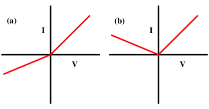
(i) Positive SC rectification: Here spin current reverses its sign under bias inversion, and here we will get positive RR. A sketch of this mechanism is given in Fig. 1(a).
(ii) Negative SC rectification: No sign reversal takes place when bias direction gets altered, as shown in Fig. 1(b), and in this situation we will get negative RR.
From these two definitions we can see that the positive SC rectification is quite similar to CC rectification as sign reversal always takes place under bias alteration for the latter one. Now, to achieve SC rectification, the symmetry between the spin current components
needs to be broken, and it is done by considering spin dependent scattering mechanisms, along with either of the above two requirements as considered for CC rectification. For our system, the finite magnetic moments associated with different lattice sites are responsible for spin separation. As SC rectification is closely related to CC rectification, it would be very interesting if one can achieve both these two types of rectifications (viz, CC and SC) simultaneously, and then a single system can be utilized for dual purposes.
Several propositions have been made so far on CC rectification, but too limited works are available on SC rectification which thus certainly demands critical analysis to probe into it further. For purposeful designing of a rectifier we need to focus not only on how to achieve higher rectification ratio ref1 ; ref2 ; ref3 ; ref4 ; ref5 ; ref6 ; ref7 ; ref8 ; ref9 ; skm1 ; kwo ; kos ; skm2 , but at the same time emphasis should be given on how its magnitude and direction can be controlled selectively ref29 ; ref29a ; ref29b ; ref29c . The present work essentially focuses on all these issues.
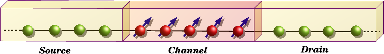
The works available in literature are mostly confined within molecular systems, quantum dots, grapheme systems, etc. ref13 ; ref14 ; ref15 ; ref16 ; ref17 ; ref18 ; ref19 ; ref20 , and interest in these systems is gradually dying out because of the fact that their performances towards rectification have already been revealed, and researchers are trying to find new functional elements for fruitful operations. The recent experimental verification of the existence of non-trivial topological features ref30 ; ref31 in diagonal and off-diagonal Harper models and the equivalence topeqi of these models with Fibonacci and other Fibonacci-like quasicrystals have motivated us to test whether any non-trivial features are obtained in the rectification operations or not. Moreover, as we can introduce quasiperiodic modulations in site energies (diagonal), in nearest-neighbor hopping (NNH) integrals (off-diagonal), or in both (generalized), we have plenty options to examine the rectification performance along with transport properties. In order to reveal these facts, in the present work, we consider a one-dimensional (1D) tight-binding (TB) chain where site energies and/or NNH integrals are modulated in the form of Harper model (also called as Aubry-André model) ref30 ; ref31 ; topeqi ; ref32 ; ref33 ; ref34 ; ref35 . Each site of the chain is accompanied by a magnetic moment (see Fig. 2) which is responsible for spin separation. As the spectrum of the system is gapped, there is a large possibility to get high degree of spin polarization at multiple energy zones associated with the separation of spin channels, which is directly reflected in the rectification operation. The gapped spectrum has strong effect on CC rectification too. The other important aspect of our model is that we have finite possibility to tune both the CC and SC RRs by regulating the phase related to site energy, or NNH integrals, or by changing both the phases of the generalized Harper model. If this tuning mechanism works successfully then it will be very important in designing suitable devices.
The rest part of the work is arranged as follows. In Sec. II we discuss the model and theoretical prescription for the calculations. All the results are critically analyzed in Sec. III, and finally, we conclude our essential findings in Sec. IV.
II Model and the Method
II.1 The Model
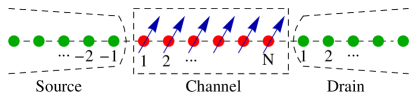
Let us start with the graphical representation of the model nano-junction, shown in Fig. 2, where a 1D chain is coupled to two semi-infinite perfect non-magnetic 1D electrodes, namely, source (S) and drain (D). We include AAH modulation in different sectors of the chain, such as site energies, or NNH integrals or both, to analyze the precise dependence of rectification operation. Each site of this chain is again accompanied by a finite magnetic moment as shown by the arrows in Fig. 2.
The Hamiltonian of the nano-junction can be written as a sum of three terms
| (1) |
where , and represent the sub-Hamiltonians of the bridging channel,
source and drain electrodes, and the tunneling coupling between the conducting channel and side attached electrodes, respectively. All these Hamiltonians are described within a TB framework.
The TB Hamiltonian for the chain, with finite magnetic moments at each lattice sites, considering the modulation both in site energies and NNH integrals reads as hm1 ; hm2 ; hm3 ,
| (2) | |||||
where
, ,
,
,
.
() is the creation (annihilation)
operator of an electron at th site with spin
() and is the NNH integral (i.e.,
hopping between and () sites). The strength of magnetic
moment at each site is denoted by , and the orientation of any such
local magnetic moment is described by the polar angle and
azimuthal angle as used in conventional polar coordinate system.
The modulations in site energies and NNH integrals are chosen as ref33 ; ref34 ; ref35
where is an irrational number and we choose it as the golden mean, and are the modulation strengths, and and are the AAH phases, which can be tuned independently with suitable setup.
Now, as voltage bias is applied between the electrodes, an electric field is established which in turn modifies the site potentials. Therefore, we can write the effective site energy as a sum of two terms ref24 ; efld1 ; efld2
| (3) |
where is the voltage independent term, and for the diagonal Harper model it becomes identical to that what is described above for . The voltage dependent term is rather very hard to determine from first principle calculations as it involves complex many-body solutions. Therefore, in our work, heuristically we can consider a potential profile in the form of a linear bias drop. This is reasonably a good choice and one can get the physical essence of rectification operation very nicely. One may also choose other potential profiles, but the fact is that all the physical pictures will remain same qualitatively. Thus, as a matter of simplification we consider only the linear bias drop along the chain, and we can express the profile for a -site chain as ref24 ; efld1 ; efld2 , where is the bias drop across the junction.
The other two sub-Hamiltonians of Eq. 1, and , will have the very simple TB forms as the electrodes are perfect and non-magnetic. These electrodes are parameterized by on-site energy and NNH integral , and they are directly coupled at the two ends of the magnetic channel with the coupling strengths and .
II.2 The Method
The common quantity that is required to describe transport properties is the transmission function. We evaluate it using wave-guide (WG) theory, a standard technique wg1 ; wg2 ; wg3 ; wg4 for calculating transmission probability. One can also use some other prescriptions like transfer-matrix formalism or Green’s function technique tm1 ; tm2 ; gn1 ; gn2 ; gn3 ; gn4 . Now, in the WG method, a set of coupled linear equations involving wave amplitudes at different lattice sites of the chain along with the boundary sites of the electrodes with which the chain is coupled are solved. Considering plane wave incidence of up and down spin electrons with unit amplitude from the source electrode, we solve the coupled equations to find the spin dependent reflection and transmission amplitudes, and , respectively. Using these quantities, we calculate reflection and transmission probabilities as and . A detailed theoretical prescription of the WG formalism is given in Appendix A. Up to now, effect of dephasing is not included in the calculations, and the inclusion of it can be understood from the other part of our work.
Once the transmission function is obtained, the spin dependent junction current is computed from the relation gn2 ; gn3
| (4) |
where is the Fermi-Dirac distribution function, and () are the electro-chemical potentials of S and D, respectively, and represents the equilibrium Fermi energy. As thermal broadening is too weak compared to the broadening caused by the conductor-to-electrode coupling, we can safely ignore the effect of temperature, and thus, throughout the analysis we set the system temperature to zero, without loss of any generality. Under this assumption the above current expression boils down to gn2 ; gn3
| (5) |
From Eq. 5 we calculate all the spin dependent currents at required bias voltages and then determine the junction charge and spin currents using the definitions and , respectively. We refer and .
Finally, we define the charge and spin current rectification ratios as ref24
| (6) |
means no rectification. As the rectification is measured by the ratios of currents in two bias polarities, sometimes it is very hard to read, and therefore we also calculate inverse of it i.e., along with .
III Results and discussion
Now, we present our essential results. The common parameter values used to carry out numerical calculations are as follows. For the side-attached 1D electrodes we choose and . The magnetic moments in the bridging chain are assumed to be aligned along the positive -direction i.e., . The conductor-to-electrode coupling strengths are chosen as asymmetric, and , and the equilibrium Fermi energy is fixed to zero. All the energies are measured in unit of electron-volt (eV), and currents are computed in unit of (). Unless otherwise stated, we do not consider the effect of dephasing right now, and we discuss it at the end of our analysis in a separate sub-section.
III.1 Ordered chain
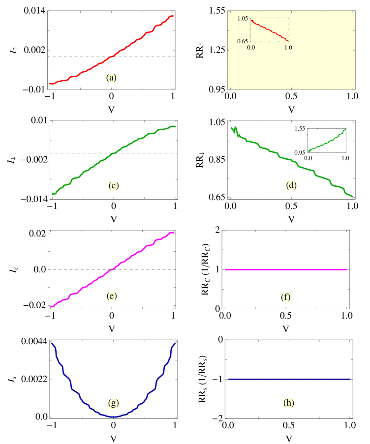
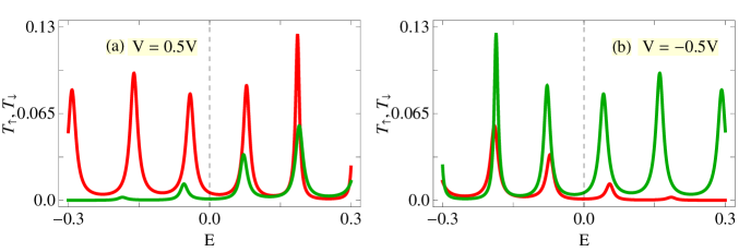
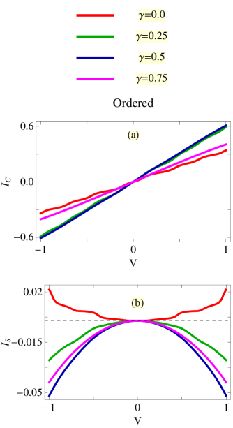
Before addressing the central results i.e., precise roles of quasiperiodic modulations on rectifications, let us first focus on the rectification operation considering a perfect chain () for the sake of illustration and to understand the basic mechanisms. The results computed for a -site chain are shown in Fig. 3, where we present spin dependent currents along with charge and spin currents, rectification ratios and the two-terminal transmission probabilities of up and down spin electrons. Several important features are observed. The individual spin current components (up and down) get unequal magnitudes (Figs. 3(a) and (c)) in two bias polarities. Therefore, finite rectification for these two spin currents are obtained as shown in Figs. 3(b) and (d). Now, looking carefully into the variations of up and down spin currents with voltage bias we see that the nature of up spin current in one bias polarity gets exactly reversed in the case of down spin current under bias reversal. Due to this fact, becomes identical with (see Figs. 3(b), (d) and their insets). From the characteristics of spin dependent currents and the corresponding rectifications, we can now easily get the dependence of charge and spin currents and the associated rectifications. Both for the charge and spin currents the magnitudes are exactly identical in two biased conditions, where the usual phase reversal is obtained in charge current, and for the case of spin current no sign alteration takes place. Accordingly, no rectification is available for charge current (), whereas spin current provides . We call it (viz, ) as full wave rectification. Here it is relevant to note that, one can get rectification, as mentioned earlier, either by considering a spatially asymmetric conductor setting identical conductor-electrode coupling (), or by considering unequal coupling () for a spatially symmetric conductor or by both. But, we see that no rectification is available for though we set asymmetric couplings of the conductor to the side attached electrodes. The reason is that we set the voltage independent site energies () to zero. Instead of this zero, if one takes any finite value then the charge current will exhibit finite rectification under this condition.
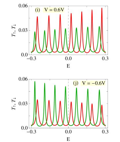
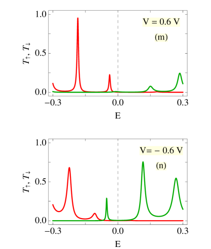
The above phenomena can be explained as follows. Let us look into the spectra given in Figs. 3(i) and (j) where we plot the transmission probabilities of up (red line) and down (green line) spin electrons for a typical bias voltage under its two polarities. Sharp resonant peaks are observed associated with the resonant energies. The interesting feature is that a perfect swapping of both the magnitude and phase takes place between the transmission probabilities of two spin components under bias alteration. It happens as we choose a perfect conductor. Now, the sign and magnitudes of individual currents (up and down), charge and spin currents as well as can be easily understood since current involves the integration of the transmission function (Eq. 5). Suppose the areas under the spectra - and - are identical (as they should be) to for any typical bias , and the areas under the curves - and - are identical to . Then the transport charge current for positive bias should be . Similarly, in the negative bias condition it becomes . Thus, getting of the identical magnitude with sign reversal for charge current under two bias polarities is clearly understood. In the same fashion we can see that i.e., no phase reversal takes place for the spin current yielding .
III.2 Diagonal AAH chain
Following the above analysis now we can explore the critical roles played by
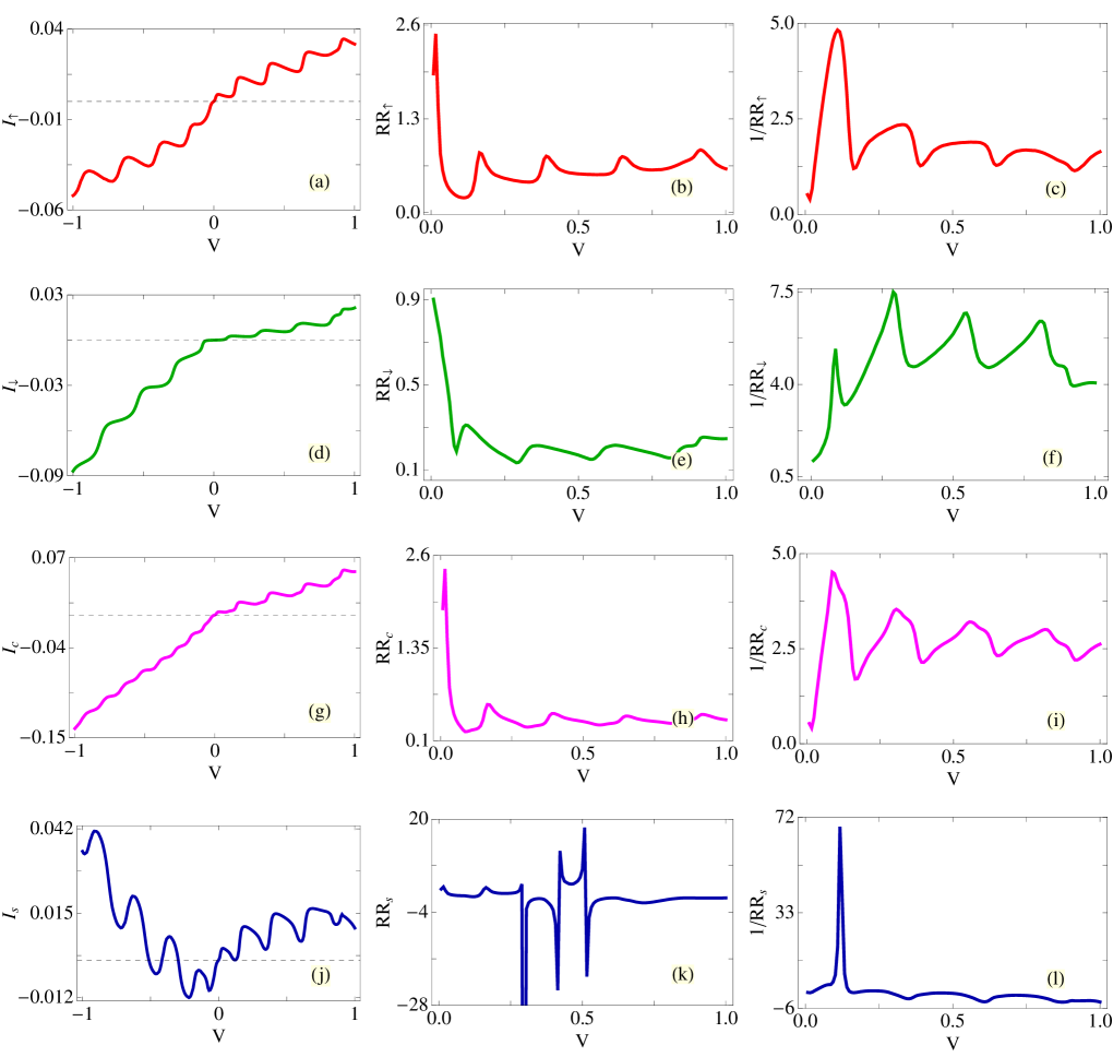
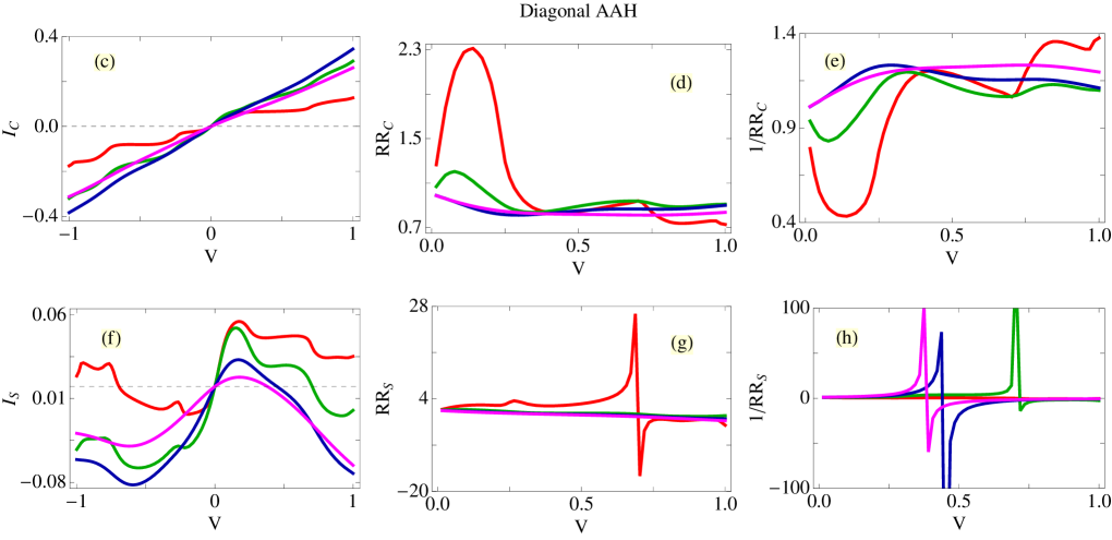
quasiperiodic modulations, in different forms, on rectifications those have not been addressed earlier in literature. To explore these facts, let us begin by considering the modulation in the diagonal part. The results are shown in Fig. 4 for a -site chain where we compute different currents, rectification ratios together with spin dependent transmission probabilities. In presence of aperiodic site energies the symmetry between two spin currents with bias alteration no longer persists, unlike the case what we get in the perfect chain. The suitable hint of getting different current amplitudes in positive and negative biases can be obtained from the nature of the transmission spectra (Figs. 4(m) and (n)), computed at a typical bias voltage. The areas under the red curves for both V are quite comparable, whereas they differ reasonably well for the green ones. These are exactly reflected in the spin dependent currents (see Figs. 4(a) and (d)). For this diagonal AAH model, the magnitudes of charge current in two bias polarities are different (Fig. 4(g)) which results a finite rectification, unlike the ordered chain, as shown in Fig. 4(h). From this figure apparently we see that reaches to at one particular (low) voltage, while it becomes too small for all other voltages. This is due to the fact that is quite large compared to the (Fig. 4(g)), and therefore when we take the inverse of , we find moderate values, as presented in Fig. 4(i). Thus, both and are required to analyze to have the complete picture of rectification. The behavior of spin current and its rectification is quite interesting (see Figs. 4(j)-(l)). Both the positive and negative spin currents are now obtained in two bias polarities, unlike the charge current, and therefore, two types of rectifications (positive and negative) are available. Also the degree of rectification is too large that is one of our primary requirements.
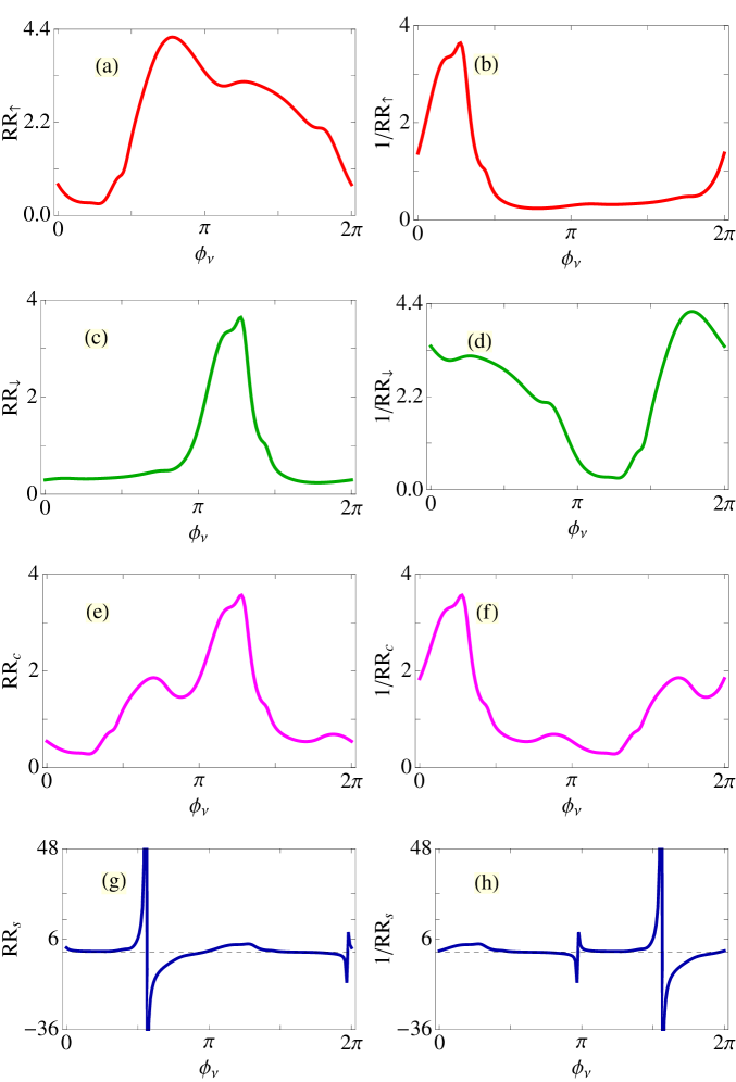
Now, to examine how the rectification operation gets changed with the modulation of quasiperiodic site energies, in Fig. 5 we show the dependence of on the diagonal AAH phase , as this phase directly modulates the site energies. The results are computed for a typical bias voltage V considering a -site diagonal AAH chain. We find a very strong dependence of on rectification. Both for the up and down spin currents, the rectification ratio and its direction can be changed widely by varying the phase . As a results of this, we get significant variation in charge and spin current rectifications. Most importantly, as this phase factor can be regulated externally with a suitable setup, we get a suitable hint of designing externally controlled efficient rectifier at nanoscale level with quasiperiodic systems. The underlying physics is that, the gapped energy spectrum of the quasiperiodic system is modified with the phase factor, which thus may produce more asymmetric density of states spectra under two different bias polarities,
resulting higher rectification. Along with these characteristics we would like to note another important feature that for the situation where (or ) is too large, then the current in any one of the two biased conditions is very high than the other one which yields half wave rectification.
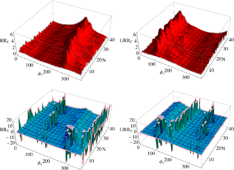
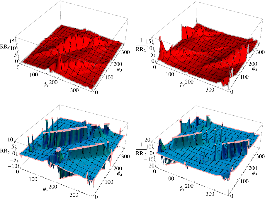
The results studied above are worked out for some typical chain lengths. In order to characterize the results for other systems sizes and at the same time to test whether there is any correlation between system size and the AAH phase , in Fig. 6 we present the variation charge and spin current rectifications as functions of and . The results are somewhat interesting and important too. At a first glance we see that charge current provides reasonably good rectification (the maximum of reaches very close to ), while for the other current (spin), the ratio is too high at some typical phases that we truncate the peaks after a certain limit for better viewing of the spectra. These high peaks essentially correspond to the half wave rectification. The other important signature is that, the results are mostly affected by the phase factor, rather than the system size. For a fixed , is almost invariant with , while change of leads to a dramatic change. Thus, we can argue that the results are robust and can be checked for a wide range of .
III.3 Off-diagonal AAH chain
Now we consider the system with AAH modulation in NNH integrals, keeping the diagonal part free from any aperiodicity. In the diagonal part we set . For this configuration, the results are rather less interesting, analogous to the perfect chain. If we look into the spectra
given in Fig. 7, we can see that the transmission probabilities of up and down spin electrons get exchanged under swapping the bias polarities. As a results of this, we cannot expect any rectification in charge current (), and for spin current the rectification ratio is always identical to and there is no question about the tuning of by means of the off-diagonal AAH phase .
III.4 Generalized AAH chain
The above analysis shows that the off-diagonal AAH model is quite trivial since on one hand it does not provide charge current rectification, and on the other hand, rectification ratio for spin current cannot be tuned anymore with the phase . But it seems trivial only due to the fact that the diagonal part is uniform. With the inclusion of incommensurate modulation in site energies, interesting phenomena can be expected. To reveal this fact look into the spectra given in Fig. 8, where we present the rectification ratios of charge and spin currents considering a generalized AAH chain, and establish the critical roles of two phases and . The one important observation is that a high degree of charge current rectification is obtained and the maximum of it reaches almost close to , which is much higher compared to the diagonal AAH model (see Figs. 6). For the case of spin current, we get quite analogous behavior like what we get in the case of diagonal AAH model. At some typical phases or is too large that we cut the peaks after a certain value for better presentation.
The key signature of this generalized AAH model is that, both charge and spin current rectifications can be controlled by tuning the diagonal and off-diagonal phases. As these phases can be regulated independently with a suitable setup, we can explore their combined effects to design an efficient nanoscale rectifier that will be used to rectify charge current and spin current as well in a tunable way.
III.5 Dephasing effect
Finally, we focus on the dephasing effect dpr1 ; dpr2 ; dpr3 which is very relevant both in the contexts of practical applications and the fundamental points of view. The main essence is to check whether the results studied here in absence of dephasing still persist and any other non-trivial features appear in presence of dephasing. Many possible sources are there that may destroy phase and spin memory of electrons, and among them the most common source is electron-phonon (e-ph) interaction. From the measurement of vibrational spectrum through inelastic tunneling spectroscopy dphexp1 ; dphexp2 it is possible to infer the strength of e-ph coupling. Roughly it is analogous to finding the position of the peaks in second-order derivative of - curve, where the voltages associated with these peaks illustrate eigenenergies of the phonons. The main challenge is how to incorporate this effect in analyzing electron transport. Though several methods are available essentially based on density functional theory (DFT) along with non-equilibrium Green’s function (NEGF) formalism dft1 ; dft2 , but most of them are too heavy and time consuming, as they require self-consistent solutions. One can circumvent these expensive methods and quantitatively explain the basic mechanisms of dephasing on transport properties by introducing the phenomenological voltage probes into the system. This is the well known Büttiker’s scattering approach dpmtd1 ; dpmtd2 ; dpmtd3 ; dpmtd4 ; dpmtd5 ; dpmtd6 , where virtual probes are incorporated at each sites of the conductor. As these are voltage probes, they do not carry any net current and they are responsible to destroy the phase memory of charge carriers. One may also use another prescription by considering reduced density matrix elements where equation of motions are illustrated in terms of Redfield equation red1 ; red2 ; red3 , but due to enormous simplicity and especially the use of minimum physical parameters, here we use Büttiker probe method to describe the dephasing effects.
We consider the virtual probes similar to real electrodes and connect them at different sites of the bridging conductor through the coupling parameter . In order to set the condition that these electrodes (virtual) are not carrying any net current, we need to choose the chemical potentials in such a way that the voltage drop across each such electrodes is zero. That can be done by applying a voltage across the real electrodes, viz, (say) and . Then the effective transmission probability becomes: .
Now come to the results shown in Fig. 9, where both the ordered and diagonal AAH chains are taken into account. For the ordered case, we get usual behavior of charge current, identical magnitudes in two bias polarities, and the overall current amplitude gets suppressed with increasing the strength of the dephasing parameter (Fig. 9(a)). On the other hand, a complete phase reversal takes place in spin current with the inclusion of dephasing, and some enhancement is also obtained. But, for this ordered chain as current magnitudes are always same in two bias polarities we cannot expect any rectification in charge current (), and full wave rectification is obtained for spin current ().
More interesting results are obtained for the AAH chain. Though, the degree of rectification gets reduced for charge current in most of the voltage regions with the addition of dephasing mechanism, for the case of spin current the scenario is quite different. From Fig. 9(g), apparently it seems that decreases with increasing , but if we take the inverse of then we see that the ratio is too high for all the dephasing strengths compared to the dephasing-free AAH chain. So there is absolutely a finite probability to get much higher rectification even in presence of dephasing, and the underlying physics for all these phenomena lies in the asymmetric nature of density of states for up and down spin bands.
IV Summary and Outlook
In summary, we have explored the possibilities of getting high degree of charge and spin current rectifications in a one-dimensional systems with quasiperiodic modulations. The quasiperiodicity is introduced in site energies and/or NNH integrals in the form of AAH model. Each site of the system sandwiched between source and drain electrodes is subjected to a finite magnetic moment which separates the up and down spin channels. As the system exhibits gapped energy energy spectrum in presence of AAH modulations, we get a large degree of rectification both in charge and spin currents in presence of an external electric field associated with the voltage bias. Unlike charge current which shows only positive rectification, we get both positive and negative rectifications in the case of spin current. We were also able to observe half and full wave rectifications, and most importantly, we get these two operations in a single system. Moreover, we have also discussed thoroughly how to tune the direction and the degree of rectification by means of both diagonal and off-diagonal AAH phases, which are extremely important factors for efficient designing a device. Finally, we have investigated the role of dephasing by incorporating Büttiker probes and found that all the characteristic features still persist even in presence of dephasing, which essentially gives us a confidence that the results presented here can be tested experimentally.
Before an end, we would like to note that to realize these models we may think about the quantum Hall system i.e., a 2D lattice in presence of transverse magnetic field where each lattice site is subjected to a finite magnetic moment. The 2D quantum Hall system exactly maps with the AAH model topeqi . Suitably tuning the magnetic field, we can easily modulate the quasiperiodicity. Here one can safely ignore the Zeeman term due to the interaction of magnetic moment with magnetic field, as band separation between two spin electrons already takes place due to the spin dependent scattering term in Eq. 2, and at the same time Zeeman term is too weak compared to this scattering. Some other prescription may be available soon to examine this model in a suitable laboratory setup. Our results undoubtedly provide some important inputs towards rectifications at nanoscale level using quasiperidic systems due to their unique gapped energy spectra.
V Acknowledgments
MP is thankful to the financial support of University Grants Commission, India (F. 2-10/2012(SA-I)) for conducting her research fellowship, and SKM would like to acknowledge the financial support of DST-SERB, Government of India (Project File Number: EMR/2017/000504).
Appendix A Wave-guide theory to evaluate transmission and reflection probabilities through a spin polarized nano-junction
To calculate reflection and transmission probabilities through the junction setup given in Fig. 10, let us begin with the wavefunction of the nano-junction
| (7) |
where the factors , and are expressed as: , , and . The coefficients , and represent the wave amplitudes of an electron having spin (, ) at th site (say) of the source, drain, and th site (say) of the channel, respectively. is the null state.
Using Eq. 7, a set of coupled linear equations are formed from the time-independent Schrödinger equation ( being the () identity matrix), and they look like,
| (8) | |||||
(i) Incidence of up spin electrons from the source end
Since the source and drain electrodes are perfect, we can write the wave
amplitudes when up spin electrons are injected from the source end as:
and
where, is the wave vector associated with the injecting electron energy
and is the lattice spacing. The other coefficients are as follows:
= transmission amplitude of a up spin transmitted
as up spin,
= transmission amplitude of a up spin transmitted
as down spin,
= reflection amplitude of a up spin reflected
as up spin,
= reflection amplitude of a up spin reflected
as down spin.
Now plugging and into the set of coupled
difference equations given in Eq. 8 and solving them, we calculate
the spin dependent reflection and transmission amplitudes for each ,
associated with the energy . Finally, we evaluate pure spin transmission
and spin flip transmission probabilities from the expressions
and
, respectively.
(ii) Incidence of down spin electrons from the source end
For the case of down spin incidence the amplitudes and
get the forms:
and
where the meaning of different quantities are:
= transmission amplitude for down spin
transmitted as up spin,
= transmission amplitude for down spin
transmitted as down spin,
= reflection amplitude for down spin
reflected as up spin,
= reflection amplitude for down spin reflected
as down spin.
In the same fashion as described above for the case of up spin electrons, we determine the reflection and transmission amplitudes for the incidence of down spin electrons using Eq. 8, and eventually, find the transmission probabilities as and .
In a similar way, one can calculate the spin dependent reflection probabilities. The method of wave-guide theory described here is the most general one, and can easily be utilized to investigate spin dependent transmission and reflection probabilities through any spin polarized nano-junction.
References
- (1) A. Aviram and M. A. Ratner, Chem. Phys. Lett. 29, 277 (1974).
- (2) V. Mujica, M. Kemp, A. Roitberg, and M. Ratner, J. Chem. Phys. 104, 7296 (1996).
- (3) V. Mujica, M. A. Ratner, and A. Nitzan, Chem. Phys. 281, 147 (2002).
- (4) C. Zhou, M. R. Deshphande, M. A. Reed, L. Jones II, and J. M. Tour, Appl. Phys. Lett. 71, 611 (1997).
- (5) C. Krzeminski, C. Delerue, G. Allan, D. Vuillaume, and R. M. Metzger, Phys. Rev. B 64, 085405 (2001).
- (6) P. E. Kornilovitch, A. M. Bratkovsky, and R. S. Williams, Phys. Rev. B 66, 165436 (2002)
- (7) F. Zahid, A. W. Ghosh, M. Paulsson, E. Polizzi, and S. Datta, Phys. Rev. B 70, 245317 (2004).
- (8) R. M. Metzger, Macromol. Symp. 212, 63 (2004).
- (9) H. Dalgleish and G. Kirczenow, Phys. Rev. B 73, 245431 (2006).
- (10) H. Dalgleish and G. Kirczenow, Phys. Rev. B 73, 235436 (2006).
- (11) G. Hu, K. He, S. Xie, and A. Saxena, J. Chem. Phys. 129, 234708 (2008).
- (12) M. Saha and S. K. Maiti, Physica E 93, 275 (2017).
- (13) G. Kwong, Z. Zhang, and J. Pan, Appl. Phys. Lett. 99, 123108 (2011).
- (14) T. Kostyrko, V. M. García-Suárez, C. J. Lambert, and B. R. Bulka, Phys. Rev. B 81, 085308 (2010).
- (15) M. Saha and S. K. Maiti, arXiv:1812.03776.
- (16) G.-C. Hu, Z. Zhang, Y. Li, J.-F. Ren, and C.-K. Wang, Chin. Phys. B 25, 057308 (2016).
- (17) G. M. Morales, P. Jiang, S. Yuan, Y. Lee, A. Sanchez, W. You, and L. Yu, J. Am. Chem. Soc. 127, 10456 (2005).
- (18) Y. Lee, B. Carsten, and L. Yu, Langmuir 25, 1495 (2009).
- (19) G.-P. Zhang, G.-C. Hu, Y. Song, Z.-L. Li, and C.-K. Wang J. Phys. Chem. C 116, 22009 (2012).
- (20) R. M. Metzger, Acc. Chem. Res. 32, 950 (1999).
- (21) J. Taylor, M. Brandbyge, and K. Stokbro, Phys. Rev. Lett. 89, 138301 (2002).
- (22) G. J. Ashwell, W. D. Tyrrell, and A. J. Whittam, J. Am. Chem. Soc. 126, 7102 (2004).
- (23) C. A. Nijhuis, W. F. Reus, and G. M. Whitesides, J. Am. Chem. Soc. 132, 18386 (2010).
- (24) S. K. Yee et al., ACS Nano 5, 9256 (2011).
- (25) A. Batra et al., Nano Lett. 13, 6233 (2013).
- (26) H. J. Yoon et al., J. Am. Chem. Soc. 136, 17155 (2014).
- (27) K. Wang, J. Zhou, J. M. Hamill, and B. Xu, J. Chem. Phys. 141, 054712 (2014).
- (28) Y. Lahini, R. Pugatch, F. Pozzi, M. Sorel, R. Morandotti, N. Davidson, and Y. Silberberg, Phys. Rev. Lett. 103, 013901 (2009).
- (29) Y. E. Kraus, Y. Lahini, Z. Ringel, M. Verbin, and O. Zilberberg, Phys. Rev. Lett. 109, 106402 (2012).
- (30) Y. E. Kraus and O. Zilberberg, Phys. Rev. Lett. 109, 116404 (2012).
- (31) S. Aubry and G. André, Ann. Isr. Phys. Soc. 3, 133 (1980).
- (32) S. Ganeshan, K. Sun, and S. Das Sharma, Phys. Rev. Lett. 110, 180403 (2013).
- (33) S. Ganeshan, J. H. Pixley, and S. Das Sarma, Phys. Rev. Lett. 114, 146601 (2015).
- (34) S. K. Maiti, S. Sil, and A. Chakrabarti, Ann. Phys. 382, 150 (2017)
- (35) A. A. Shokri and M. Mardaani, Solid State Commun. 137, 53 (2006)
- (36) M. Dey, S. K. Maiti, and S. N. Karmakar, Eur. Phys. J. B 80, 105 (2011).
- (37) M. Patra and S. K. Maiti, Europhys. Lett. 121, 38004 (2018).
- (38) S. Pleutin, H. Grabert, G. L. Ingold, and A. Nitzan, J. Chem. Phys. 118, 3756 (2003).
- (39) S. K. Maiti and A. Nitzan, Phys. Lett. A 377, 1205 (2013).
- (40) Y. Shi and H. Chen, Phys. Rev. B 60, 10949 (1999).
- (41) Y. J. Xiong and X. T. Liang, Phys. Lett. A 330, 307 (2004).
- (42) M. Patra and S. K. Maiti, Sci. Rep. 7, 43343 (2017).
- (43) M. Patra and S. K. Maiti, Sci. Rep. 7, 14313 (2017).
- (44) H. Xu, Phys. Rev. B 50, 8469 (1994).
- (45) K. Yakubo, Comput. Phys. Commun. 142, 429 (2001).
- (46) D. S. Fisher and P. A. Lee, Phys. Rev. B 23, 6851 (1981).
- (47) S. Datta, Electronic Transport in Mesoscopic Systems, Cambridge University Press, Cambridge (1997).
- (48) S. Datta, Quantum Transport: Atom to Transistor, Cambridge University Press, Cambridge (2005).
- (49) S. K. Maiti, J. Appl. Phys. 117, 024306 (2015).
- (50) D. Nozaki, Y. Girard, and K. Yoshizawa, J. Phys. Chem. C 112, 17408 (2008).
- (51) C. J. Cattena, R. A. Bustos-Marun, and H. M. Pastawski, Phys. Rev. B 82, 144201 (2010).
- (52) D. Nozaki, C. G. da Rocha, H. M. Pastawski, and G. Cuniberti, Phys. Rev. B 85, 155327 (2012).
- (53) B. C. Stipe, M. A. Rezaei, and W. Ho, Science 280, 1732 (1998).
- (54) W. Wang, T. Lee, I. Kretzschmar, and M. A. Reed, Nano Lett. 4, 643 (2004).
- (55) N. Sergueev, D. Roubtsov, and H. Guo, Phys. Rev. Lett. 95, 146803 (2005).
- (56) N. Sergueev, A. A. Demkov, and H. Guo, Phys. Rev. B. 75, 233418 (2007).
- (57) M. Büttiker, Phys. Rev. Lett. 57, 1761 (1986).
- (58) M. Büttiker, Phys. Rev. B 33, 3020 (1986).
- (59) M. Büttiker, IBM J. Res. Dev. 32, 63 (1988).
- (60) J. Maassen, F. Zahid, and H. Guo, Phys. Rev. B 80, 125423 (2009).
- (61) M. Dey, S. K. Maiti, and S. N. karmakar, Org. Electron. 12, 1017 (2011).
- (62) T.-R. Pan, A.-M. Guo, and Q.-F. Sun, Phys. Rev. B 92, 115418 (2015).
- (63) A. K. Felts, W. T. Pollard, and R. A. Friesner, J. Phys. Chem. 99, 2929 (1995).
- (64) D. Segal, A. Nitzan, W. B. Davis, M. R. Wasielewski, and M. A. Ratner, J. Phys. Chem. B 104, 3817 (2000).
- (65) D. Segal, A. Nitzan, M. Ratner, and W. B. Davis, J. Phys. Chem. B 104, 2790 (2000).