Some Interesting Features of Memristor CNN
Makoto Itoh111After retirement from Fukuoka Institute of Technology, he has continued to study the nonlinear dynamics on memristors.
1-19-20-203, Arae, Jonan-ku,
Fukuoka, 814-0101 JAPAN
Email: itoh-makoto@jcom.home.ne.jp
In this paper, we introduce some interesting features of a memristor CNN (Cellular Neural Network).
We first show that there is the similarity between the dynamics of memristors and neurons.
That is, some kind of flux-controlled memristors can not respond to the sinusoidal voltage source quickly,
namely, they can not switch “on” rapidly.
Furthermore, these memristors have refractory period after switch “on”, which means that it can not respond to further sinusoidal inputs until the flux is decreased.
We next show that the memristor-coupled two-cell CNN can exhibit chaotic behavior.
In this system, the memristors switch “off” and “on” at irregular intervals,
and the two cells are connected when either or both of the memristors switches “on”.
We then propose the modified CNN model, which can hold a binary output image, even if all cells are disconnected and no signal is supplied to the cell after a certain point of time.
However, the modified CNN requires power to maintain the output image, that is, it is volatile.
We next propose a new memristor CNN model.
It can also hold a binary output state (image), even if all cells are disconnected, and no signal is supplied to the cell, by memristor’s switching behavior.
Furthermore, even if we turn off the power of the system during the computation, it can resume from the previous average output state, since the memristor CNN has functions of both short-term (volatile) memory and long-term (non-volatile) memory.
The above suspend and resume feature are useful when we want to save the current state, and continue work later from the previous state.
Finally, we show that the memristor CNN can exhibit interesting two-dimensional waves, if an inductor is connected to each memristor CNN cell.
Keywords: memristor CNN; non-volatile; chaotic behavior; suspend and resume feature; long-term memory; short-term memory; two-dimensional wave; switch; neuron; synapse; excitatory; inhibitory; refractory period.
1 Introduction
In this paper, we introduce some interesting features of a memristor CNN (Cellular Neural Network).222The terminology CNN was originally used for Cellular Neural Network [1, 2]. Recently, CNN is also used for Convolutional Neural Network. In this paper, CNN stands for Cellular Neural Network. We first study the switching behavior of flux-controlled memristors. The flux-controlled memristor switches “off” and “on”, depending on the value of the flux. Some kind of flux-controlled memristors cannot respond to the sinusoidal voltage source quickly. That is, it cannot switch “on” rapidly. Furthermore, these memristors have refractory period after switch “on”, that is, it can not respond to further sinusoidal inputs until the flux is decreased. We also show that the memristor-coupled two-cell can exhibit chaotic behavior. In this system, the memristors switch “off” and “on” at irregular intervals, and the two cells are connected when either or both of the memristors switches “on”.
We next propose the modified CNN and the memristor CNN. The modified CNN can hold a binary output image even if all cells are disconnected and no signal is supplied to the cell after a certain point of time. The modified CNN requires power to maintain the output image, that is, it is volatile. We can realize the above switching behavior by using flux-controlled memristors, since the memristor can switch “off” and “on”, depending on the value of the flux. The memristor CNN can also hold a binary output image, even if all cells are disconnected, and even if no signal is supplied to the cell, by memristor’s switching behavior. However, it also requires power to maintain the output image, since the nonlinear element (nonlinear resistor) of the CNN cell are volatile.
It is well-known that the neurons can not respond to inputs quickly and they cannot generate outputs rapidly, since charging or discharging the membrane potential energy can take time. Furthermore, after firing, the neurons have refractory period. We show that the image processing (visual computing) of the memoristor CNN can exhibit the similar behavior, if the memductance of the flux-controlled memristor has twin-peaks.
The suspend and resume feature are useful when we want to save the current state, and continue work later from the same state. We show that the memristor CNN has this kind of feature. That is, even if we turn off the power of the memristor CNN during the computation, it can recover the average output state later, by using the non-volatile memristors. Furthermore, it can resume from the previous average output.
In our brain’s system, a long-term memory is a storage system for storing and retrieving information. A short-term memory is the short-time storage system that keeps something in mind before transferring it to a long-term memory. We also show that the memristor CNN has functions of the short-term and long-term memories.
Finally, we show that the memristor CNN can exhibit interesting two-dimensional waves, if an inductor is connected to each memristor CNN cell. In this case, the dynamics of the CNN cell is given by the nd-order differential equation.
2 Basic Notations and Definitions
In this section, we introduce some basic notations and definitions which will be used later.
2.1 Cellular Neural Networks
Cellular Neural Network (CNN) [1, 2, 3, 4] is a dynamic nonlinear system defined by coupling only identical simple dynamical systems, called cells, located within a prescribed sphere of influence, such as nearest neighbors. The dynamics of a standard cellular neural network with a neighborhood of radius are governed by a system of differential equations
Dynamics of the CNN
(1)
where , , , are called state, output, input, and threshold of cell , respectively. denotes the -neighborhood of cell , and , and denote the feedback, control, and threshold template parameters, respectively. The output and the state of each cell are usually related via the piecewise-linear saturation function
| (2) |
The matrices and are referred to as the feedback template and the feedforward (input) template , respectively. If we restrict the neighborhood radius of every cell to , then the cell is coupled only to its eight neighbor cells , where
| (3) |
Assume that is the same for the whole network, that is, , and set for the sake of simplicity. Then, the template is fully specified by parameters, which are the elements of two matrices and , namely
| (4) |
and a real number . The output and input for the cell cell are specified by
| (5) |
Here, we assumed that the feedback parameters and the control template parameters do not vary with space, that is, they can be defined as [1, 2]
| (6) |
For example,
| (7) |
Thus, we obtained the four elements:
| (8) |
in Eq. (4). Similarly, we can obtain all other elements of templates and .
The CNN template is usually designed such that the qualitative behavior is not affected by the small perturbation of the template. If the CNN template satisfies this property, then the output image remains unchanged, even if we change the template parameters slightly. It also remains unchanged in the presence of sufficiently small noise.
Many applications of the CNN templates are to convert gray-scale images to binary images. In this paper, the luminance value of the pixel would be coded as black , white , gray . Furthermore, in order to simulate Eq. (1) in a computer, the initial condition and the boundary condition must be specified. For example, the fixed boundary condition is given by
| (9) |
where denotes boundary cells, and and are constants.
Finally, let us consider an isolated CNN cell, which does not have the inputs, the outputs from other cells, and the threshold, for later use. Its dynamics is given by the first-order differential equation:
| (10) |
where is the feedback parameter. The output and the state of the isolated cell is related by
| (11) |
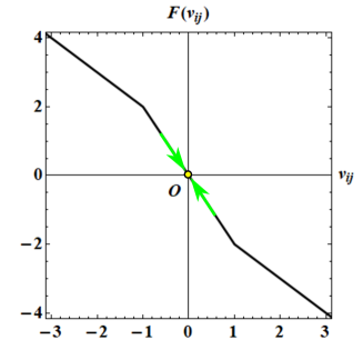
Assume . Then Eq. (10) has three equilibrium points, one is unstable and others are stable [1]. We study its detailed behavior in Sec. 4.1.
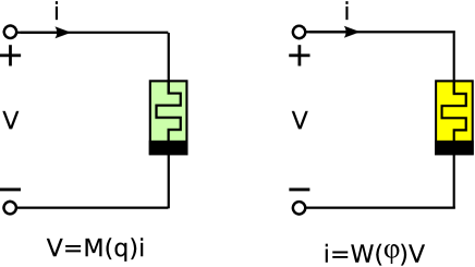
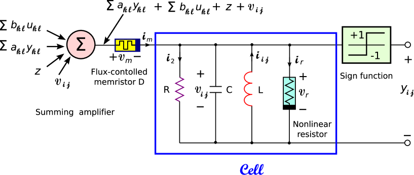
2.2 Memristors
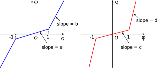
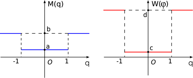
The memristor shown in Figures 1-3 is a passive 2-terminal electronic device described by a nonlinear relation
| (12) |
between the charge and the flux [5, 6]. Its terminal voltage and the terminal current is given by
characteristic of memristors
(13)
where
(14)
The two nonlinear functions and , called the memristance and memductance, respectively, are defined by
| (15) |
and
| (16) |
representing the slope of a scalar function and , respectively, called the memristor constitutive relation.
A memristor characterized by a differentiable (resp., ) characteristic curve is passive if, and only if, its small-signal memristance (resp., small-signal memductance ) is nonnegative (see [5]). Since the instantaneous power dissipated by the above memristor is given by
| (17) |
or
| (18) |
the energy flow into the memristor from time to satisfies
| (19) |
for all .
In this paper, we assume the followings unless otherwise noted:
1. The memristor is ideal, that is, it is endowed with a nonvolatility property. 2. The passive memristor will not lose its flux or charge via the parasitic elements when we switch off the power.

3 Neuron-like Response of Memristors
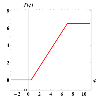
Consider the two-element circuit shown in Figure 4. It consists of a flux-controlled memristor and a periodic voltage source , where . The constitutive relation of the flux-controlled memristor is given by
| (20) |
where , (see Figure 5(a)), and the flux is defined by
| (21) |
The memductance is given by
| (22) |
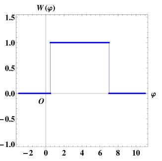
where denotes the unit step function, equal to for and 1 for . Thus, the memristor switches “off” and “on”, depending on the value of the flux as shown in Figure 5(b). Its terminal voltage and the terminal current satisfy
| (23) |
where
| (24) |
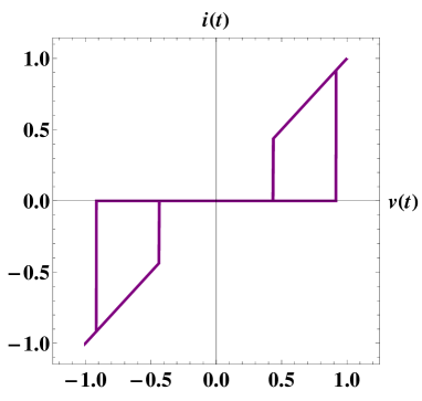
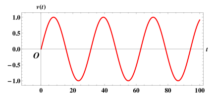
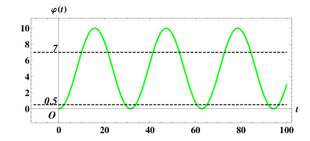
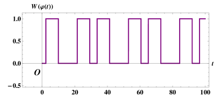
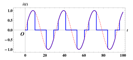
We show the pinched hysteresis loop of flux-controlled memristor in Figure 6. We also show the waveforms of the terminal voltage , the terminal current , the flux , and the memductance in Figure 7. Observe that the current flows through the memristor if and no current flows through the memristor if and as shown in Figure 7(c), since the memristor switches “off” and “on”, depending on the value of the flux as shown in Figure 7(c).
There is the similarity between memristors and neurons.
That is, the neurons cannot respond to inputs quickly and they cannot generate outputs rapidly.
Charging or discharging the membrane potential energy can take time.
Furthermore, after firing, the neurons have refractory period (the period during which the neurons can not respond to further stimulation).
Thus, we conclude as follow:
The flux-controlled memristor defined by Eq. (23) cannot respond to the sinusoidal voltage source quickly. That is, it cannot switch “on” rapidly. Furthermore, this memristor has refractory period after switch “on”, that is, it can not respond to further sinusoidal inputs until the flux is decreased.
 |
 |
| (a) constitutive relation | (b) memductance |
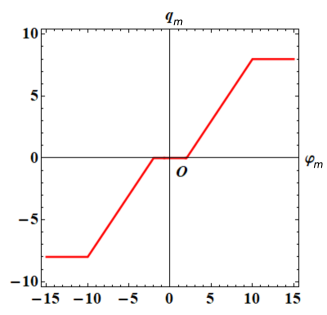
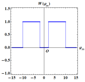
(a) The constitutive relation of the memristor, which is given by .
(b) Memductance of the memristor, which is defined by . Thus, for , and for and .
 |
| (a) driving source |
 |
| (b) flux |
 |
| (c) memductance |
 |
| (d) current |
(a) Waveform of the driving source , which is defined by , where .
(b) Waveform of the flux across the memristor, which is defined by .
(b) Waveform of the memductance , which is defined by .
(d) Waveform of the current through the memristor, which is defined by (blue). Red dashed line denotes the waveform of the driving source .
4 Chaotic Oscillation from Memristor-Coupled CNNs
It is well known that an autonomous two-cell CNN exhibits a limit cycle, and a second-order non-autonomous CNN exhibits a chaotic attractor [1, 2]. In this paper, we show that a non-autonomous memristor-coupled CNN can also exhibit a chaotic attractor.
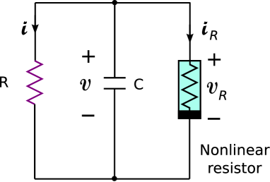
4.1 Isolated CNN cell
An isolated CNN cell, without the inputs, the outputs from other cells, and the threshold, can be realized by the circuit in Figure 8. The dynamics of this circuit is given by
| (25) |
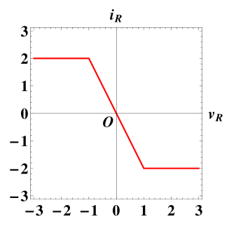
where . The characteristic of the nonlinear resistor is given by
| (26) |
where is a constant. If , then the nonlinear resistor is active as shown in Figure 9. Substituting Eq. (26) into Eq. (25), we obtain
| (27) |
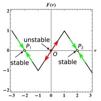
If , then Eq. (27) has three equilibrium points. The two equilibrium points are located on both sides of the origin, and they are stable. The other one is the origin , which is unstable. For example, if , then the equilibrium points and are stable and the origin is unstable, as shown in Figure 10. Thus, we obtain
| (28) |
The above behavior will be used in Sec. 5.
Equations (25) and (27) can be recast into the well-known first-order equation of the standard isolated CNN cell
Dynamics of isolated CNN cell
(29)
where and (see Eq. (10)).
4.2 Non-autonomous two-cell CNNs
Let us consider the non-autonomous two-cell CNN in Figure 11 [1]. It is driven by an independent current source. The dynamics of the circuit is given by
| (30) |
where
| (31) |
In this circuit, the two nonlinear resistors have the same current-voltage characteristics, that is,
| (32) |
The two voltage-controlled current sources are defined by
| (33) |
Equation (30) is recast into the second-order non-autonomous CNN equation [1]:
Dynamics of non-autonomous CNN
(34)
where , and
| (35) |
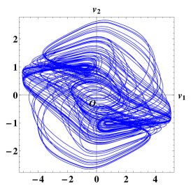
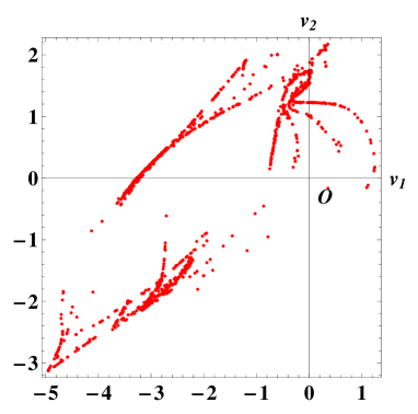
We show the well-known chaotic trajectory and the associated Poincaré map of Eq. (30) in Figure 12 [1].
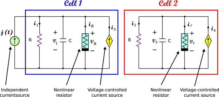
(1) The two nonlinear resistors (cyan) have the same current-voltage characteristics: (left) and (right).
(2) The two voltage-controlled current sources (yellow) are defined by (left) and (right).
 |
 |
| (a) Chaotic trajectory on the -plane | (b) Associated Poincaré map |
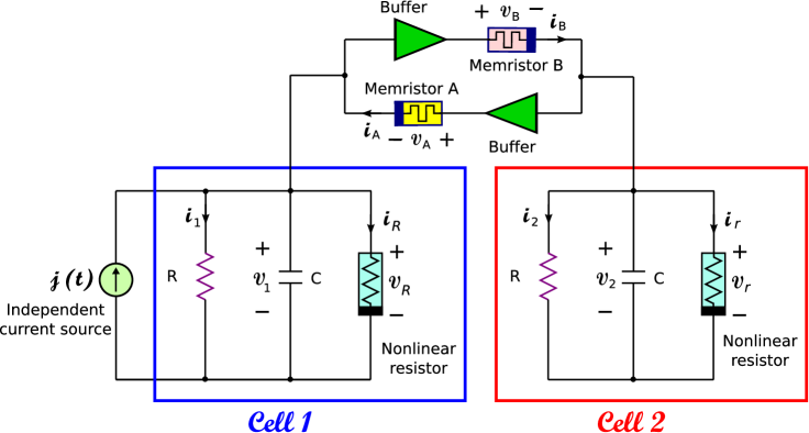
(1) Parameters: .
(2) The cell 1 (left) is driven by an independent current source (light-green): .
(3) The memristor (yellow) is passive, while the memristor (pink) is active.
(4) The terminal currents and voltages of the memristor and the memristor satisfy and , respectively, where , , , and .
The symbol denotes the unit step function, equal to for and 1 for .
(5) The two nonlinear resistors (cyan) have the same current-voltage characteristics, that is, and .
(6) The buffer (dark green) is a op-amp circuit which has a voltage gain of , that is, the output voltage is the same as the input voltage. It offers input-output isolation.
4.3 Memristor-coupled two-cell CNNs
Let us consider the non-autonomous CNN in Figure 13, whose cells are coupled with memristors. The dynamics of the circuit in Figure 13 is given by
| (36) |
where
| (37) |
Here, and denote the flux of the memristors and , respectively, and denote the memductances of the memristors and , respectively, denotes an independent current source, and denotes the unit step function, equal to for and 1 for . The two nonlinear resistors have the same current-voltage characteristics, that is,
| (38) |
The terminal currents and voltages of the memristors and satisfy the relation
| (39) |
respectively.
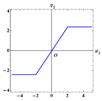
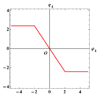
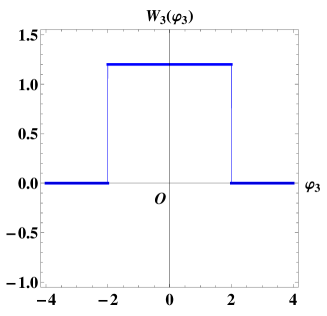
We show the constitutive relations and memdauctances of the flux-controlled memristors in Figures 14 and 15, respectively. Equation (36) is recast into the form:
Dynamics of memristor-coupled two-cell CNN
(40)
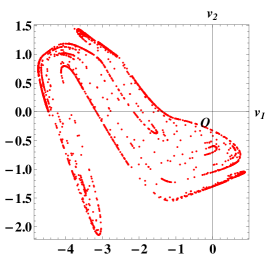
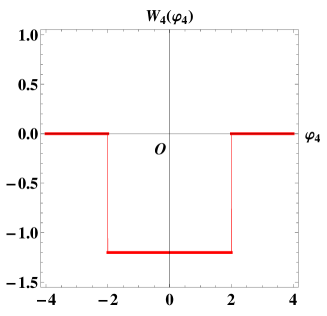
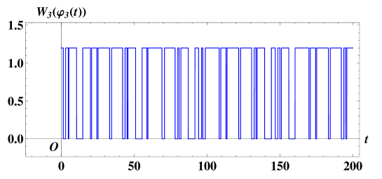
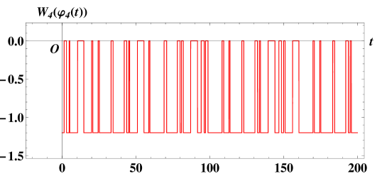
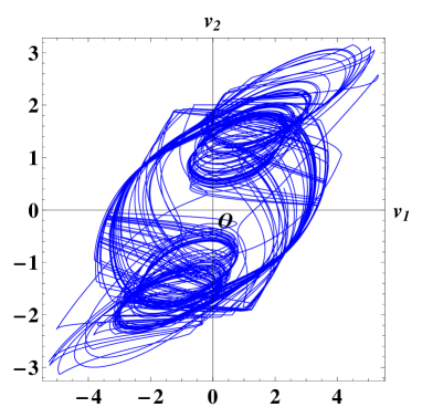
Note that the memristor is active since . On the contrary, the memristor is passive since . Observe that the memristors switch “off” and “on” at irregular intervals as shown in Figure 16. Furthermore, the two cells are connected when either or both of the memristors switches “on”. We show the trajectory of Eq. (36) and its associated Poincaré map in Figure 17. Observe that Eq. (36) can exhibit a chaotic attractor. Thus, we conclude as follow:
The non-autonomous memristor-coupled two-cell CNN defined by Eq. (36) can exhibit a chaotic attractor. The two flux-controlled memristors in Figure 13 switch “off” and “on” at irregular intervals. Furthermore, the two cells are connected when either or both of the memristors switches “on”.
 |
 |
| (a) passive memristor | (b) active memristor |
 |
 |
| (a) | (b) |
 |
| (a) |
 |
| (b) |
4.4 Similarity between memristors and neurons
In this subsection, we show that there is the similarity between memristors and neurons. The neuron has an “excitatory” synapse and an “inhibitory” synapse. Synapses are junctions that allow a neuron to transmit a signal to another cell. They can either be excitatory or inhibitory. The inhibitory synapses decrease the likelihood of the firing action potential of a cell, while the excitatory synapses increase its likelihood of the firing action potential of a cell.
The memristors in Figure 13 transmit signals from one cell to another cell at irregular intervals. The instantaneous powers of the memristor and are given by
| (41) |
and
| (42) |
respectively, where and .
It follows that the instantaneous power flows into the cell 2. Similarly, the instantaneous power flows into the cell 1 with the current source , that is, flows out of it, since is negative.333Note the direction of the power flow and the buffer in Figure 13 provides an input-output isolation. Thus, the memristor corresponds to the “excitatory synapse”, and the memristor corresponds to the “inhibitory synapse”. The chaotic oscillation of Eq. (36) depends on a delicate balance between the powers and .
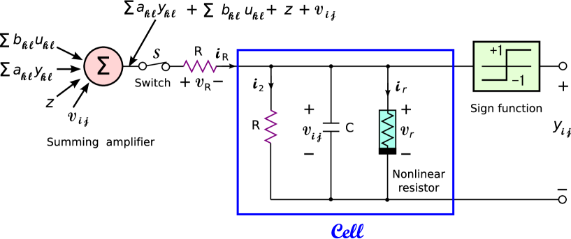
(1) Parameters: .
(2) The characteristic of the nonlinear resistor (light blue) is given by , where is a constant.
(3) The output voltage of the summing amplifier is given by .
(4) The above output voltage contains the voltage of the capacitor (the last term).
(5) The above sum does not contain the term ().
(6) The output and the state of each cell are related via the sign function (green): .
(7) The two linear resistors (purple) have the same resistance . Thus, we used the same symbol and color.
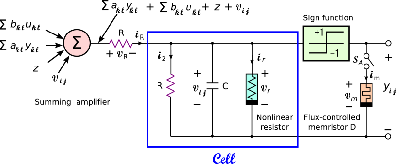
5 Modified CNN
Consider the modified CNN shown in Figure 18. In this system, the output and the state of each cell is related via the sign function444The sign function can be approximated by using the saturation non-linearity of the Op amp, and by normalizing its output voltage.
| (43) |
The switch is used to disconnect all signals, namely, the output , the input , the threshold , and the state .
Let us calculate the voltage across the resistor , which is connected to the switch . It is given by
| (44) |
Thus, the dynamics of the modified CNN is given by
| (45) |
where
-
(a)
.
-
(b)
denotes the voltage across the capacitor .
-
(c)
The symbols and denote the output and input of cell , respectively.
-
(d)
The symbol denotes the -neighborhood of cell .
-
(e)
The symbols , and denote the feedback, control, and threshold template parameters, respectively. The matrices and are referred to as the feedback template and the feed-forward (input) template , respectively.
- (f)
Substituting Eq. (46) into Eq.(45), and using the relations , , , we obtain
Dynamics of the modified CNN
(47)
If we restrict the neighborhood radius of every cell to , and if we assume that the feedback and control template parameters do not vary with space, then the template is fully specified by parameters, which are the elements of two matrices and , namely
| (48) |
and a real number [1, 2]. As stated in Sec. 2.1, the feedback and control template parameters can be described as follow:
| (49) |
5.1 Template parameter
The following sum in Eq. (47):
| (50) |
does not contain the term:
| (51) |
Substituting Eq. (49) into the left-hand side of Eq. (51), we obtain
| (52) |
Thus, is not included in Eq. (50). That is, the element of the feedback template in Eq. (48) is not given. Therefore, we define by setting , where is the parameter of the nonlinear resistor, which is given by Eq. (46).
Element of template
The element of the feedback template is defined by
(53)
where is the parameter of the nonlinear resistor defined by
(54)
The other elements of are defined by the coefficients of the output , that is,
(55)
5.2 Gray-scale edge detection
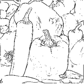
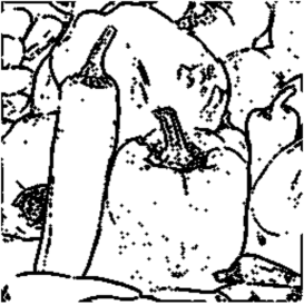
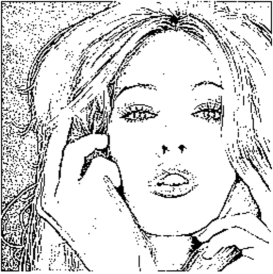
Let us consider the gray-scale edge detection template [1, 2]
| (56) |
The initial condition for is given by
| (57) |
and the input is equal to a given gray scale image. The boundary condition is given by
| (58) |
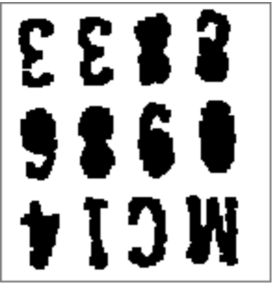
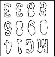
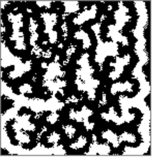
where denotes boundary cells. This template can extract edge of objects in gray scale image as shown in Figure 19. Observe that the modified CNN (47) can hold a binary output image, even if the switch in Figure 18 is turned off at . That is, the output binary state can not be changed by switching off.
5.3 Shadow projection
| (59) |
The initial condition for is given by
| (60) |
and the input is equal to a given binary image. The boundary condition is given by
| (61) |
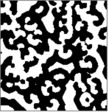
where denotes boundary cells. This template can project onto the left shadow of all objects illuminated from the right as shown in Figure 20. Observe that the modified CNN (47) can hold a binary output image, even if the switch is turned off at . That is, the output binary state can not be changed by switching off as stated above.
 |
 |
 |
| (a) input image | (b) output image () | (c) output image () |
| before switch off | after switch off |
 |
 |
 |
| (a) input image | (b) output image () | (c) output image () |
| before switch off | after switch off |
5.4 Behavior of the isolated cell after switch-off
Assume that the switch in Figure 18 is turned off at . Then, the dynamics of the cell is given by
| (62) |
Let us study the behavior of Eq. (62) for the three cases: , , and .
-
1.
Case 1. .
The driving-point plot of Eq. (62) for is shown in Figure 10. From Eq. (28), we obtain(63) where . Since the solution can not move across the origin, the output satisfies the following relations:
(64) where . Thus, the output binary state can not be changed even if we turn off the switch at .
-
2.
Case 2. .
We show the driving-point plot of Eq. (62) for in Figure 21. Observe that the origin is a stable equilibrium point. Thus, any trajectory tends to the origin, that is, as . Since the solution for can not move across the origin, Eq. (64) also holds. That is, the output does not change (except for ), even if we turn off the switch at . -
3.
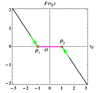
Case 3. .
We show the driving-point plot of Eq. (62) for in Figure 22. Observe that Eq. (62) has an invariant set . Any trajectories outside of tends to the boundary of this set. Furthermore, the solution for can not move across . Thus, Eq. (64) also holds, that is, the output binary state can not be changed even if we turn off the switch at .
We conclude that the modified CNN (47) can hold a binary output image even if all cells are disconnected from the summing amplifier and no signal is supplied to the cell. However, we should assume that . It is due to the reason that if , then the physical circuit, for example, the sign function circuit, may not work properly in the presence of noise when becomes sufficiently small. Furthermore, if , then the qualitative behavior of Eq. (62) is greatly changed by the small perturbation of .
Note that the modified CNN requires power to maintain the output image, since the isolated cell has a nonlinear active resistor. That is, the output image is lost immediately (volatile) when the power is interrupted. From our computer simulations666If the input image size is , we have to solve a system of 65536 first-order differential equations. Thus, we used the simple Euler method for solving Eq. (47). It is the most basic method for numerical integration., we obtain the following result:
Assume . Then the modified CNN (47) can hold a binary output image even if all cells are disconnected from the summing amplifier and no signal is supplied to the cell after a certain point of time. The modified CNN requires power to maintain the output image, that is, it is volatile.
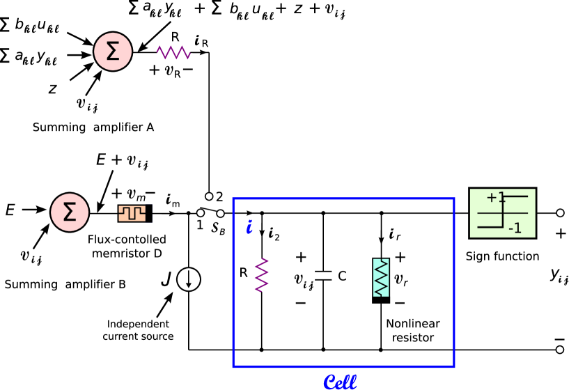
6 Memoristor CNN
The memristor can switch “off” and “on”, depending on the value of the flux. In this section, we realize the switch in Figure 18 by using memristors.
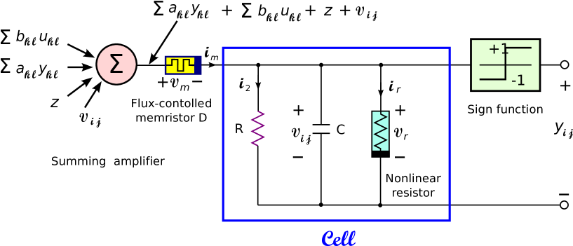
(1) Parameters: .
(2) The characteristic of the nonlinear resistor (light blue) is given by , where is a constant.
(3) The terminal currents and voltages of the flux-controlled memristor (yellow) satisfies , where for , and for and .
(4) The output voltage of the summing amplifier (pink) is given by .
(5) The above output voltage contains the voltage of the capacitor (the last term).
(6) The above sum does not contain the term ().
(7) The output and the state of each cell are related via the sign function (green): .
Consider the circuit shown in Figure 23. The dynamics of this circuit is given by
| (65) |
where , and the symbols , , and denote the voltage across the capacitor , the current through the nonlinear resistor, and the current through the memristor, respectively. Furthermore, this circuit satisfies the following relations:
-
(a)
The output and the state of each cell is related via the sign function
(66) -
(b)
The characteristic of the nonlinear resistor is given by
(67) where is a constant.
-
(c)
The terminal voltage and the terminal current of the memristor is given by
(68) where the flux of the memristor is defined by
(69) -
(d)
The voltage across the memristor is given by
(70) Note that the first term does not contain , where .
-
(e)
Each cell has only one memristor.
Substituting Eqs. (67), (68) into Eq. (65), and using the relations , , we obtain
Dynamics of the memristor CNN
(71)
As stated in Sec. 2.1, if we restrict the neighborhood radius of every cell to , and if we assume that the feedback and control template parameters do not vary with space, then the templates are fully specified by parameters, which are the elements of two matrices and , namely
|
|
(72) |
and a real number , where ( is the parameter of the nonlinear resistor defined by Eq. (67)).777 The term is not included in Eq. (70), as shown in Sec. 5. Therefore, we have to define the element of the template by setting .
6.1 Dilation
Let us consider the dilation template [1, 2]
| (73) |
The initial condition for is given by
| (74) |
and the input is equal to a given binary image. The boundary condition is given by
| (75) |
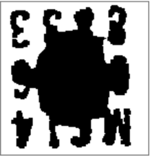
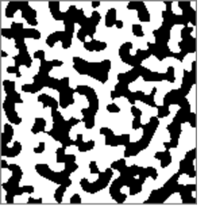
where denotes boundary cells. This template can be used to grow a layer of pixels around objects.
Assume that the memductance is given by
| (76) |
The constitutive relation and memductance of the memristor is shown in Figure 24. The terminal voltage satisfies
| (77) |
where . For example, assume that
| (78) |
Then, we obtain
| (79) |
From Eq. (69), we obtain
| (80) |
where we assumed . Thus,
| (81) |
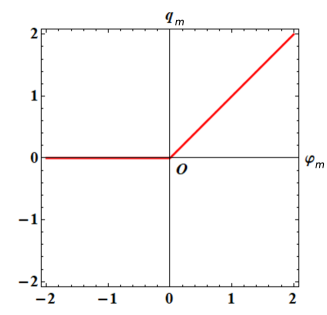
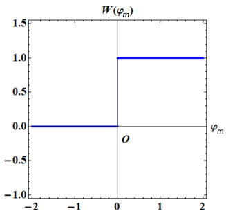
Hence, the memristor switches “off” for . Our computer simulations are given in Figure 25. Observe that the template (73) can be used to grow a layer of pixels around objects. It can hold a binary output image for , at which all memristors switched “off”. Note that all memristors do not switch “off” synchronously since their terminal flux are not always identical.
 |
 |
| (a) constitutive relation | (b) memductance |
(a) The constitutive relation of the memristor, which is given by .
(b) Memductance of the memristor, which is defined by . Thus, for , and for and .
 |
 |
 |
| (a) input image | (b) output image before all | (c) output image after all |
| memristors turned off () | memristors turned off () |
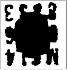
6.2 Sharpening with binary output
Let us consider the sharpening with binary output template
| (82) |
The initial condition for is given by
| (83) |
and the input is equal to a given gray-scale image. The boundary condition is given by
| (84) |
where denotes boundary cells. This template can be used to make an image appear sharper by enhancing edges and convert into a binary image.
Assume that the memductance is given by Eq. (76). The constitutive relation and memductance of the memristor is shown in Figure 24. The terminal voltage satisfies
| (85) |
where (gray-scale image). Thus, if becomes zero at , then and does not change until for . In this case, all memristor may not switch “off”.
We show our computer simulations in Figure 26. Observe that the template (82) can make the image sharper by enhancing edges and convert into a binary image. Thus, the memoristor CNN (65) can hold a binary output image, even if almost memristos switched “off” as shown in Figure 26(c). Thus, we conclude as follow:
Assume . Then the memristor CNN in Figure 23 can hold a binary output image, even if almost all memristors switch off.
 |
 |
 |
| (a) input image | (b) output image at | (c) disconnected cells at |
| (printed in blue) |
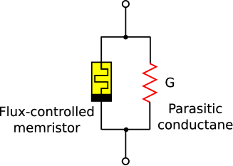
7 Effect of a Parasitic Conductance
Consider the case where the memristor in Figure 23 has a parallel parasitic conductance as shown in Figure 27. Then, the dynamics of the circuit in Figure 23 is modified into
| (86) |
where , and the symbols , , , and denote the voltage across the capacitor , the current through the memristor, and the current trough the nonlinear resistor, and the current through the parallel parasitic conductance , respectively.
Furthermore, this circuit satisfies the following relations:
-
(a)
The output and the state of each cell is related via the sign function
(87) -
(b)
The voltage across the memristor is given by
(88) where the first sum does not contain , where . The current through the memristor is given by
(89) where denotes the memductance of the memristor and the flux of the memristor is defined by
(90) -
(c)
The current through the conductance is given by
(91) where .
-
(d)
The characteristic of the nonlinear resistor is given by
(92) where is a constant.
Substituting Eqs. (89), (91), and (92) into Eq. (86), we obtain
| (93) |
Let us assume that the memductance is given by Eq. (76), that is,
| (94) |
Then the dynamics of Eq. (93) can be described as follow:
-
1.
Case 1. .
From Eq. (93), we obtain(95) where . Substituting Eq. (70) into Eq. (95), we obtain
(96) Assume that the qualitative behavior of the modified CNN (47) is not affected by the small perturbation of the template . Then the output of Eq. (96) is identical to that of the modified CNN, which is given by
(97)
-
2.
Case 2. .
From Eq. (93), we obtain(98) where . Let us choose the parameter so that the qualitative behavior of the isolated cell is not affected by the small perturbation . For example, choose . Then, the qualitative behavior of the driving-point plot of Eqs. (95) and (98) is not changed, since and have the same sign. Thus, the output is not changed by this small perturbation . In this case, Eq. (98) is approximated by
(99)
It follows that there is not much of a difference between the output images of Eqs. (65) and (86). Note that the CNN template is usually designed such that the qualitative behavior is not affected by the small perturbation. In fact, we could not find any difference between the output images of Eqs. (65) and (86) when the template is given by Eq. (73) or Eq. (82). Thus, we conclude as follow:
8 Neuron-like Behavior
The neurons cannot respond to inputs quickly and they cannot generate outputs rapidly, since charging or discharging the membrane potential energy can take time. Furthermore, after firing, the neurons have refractory period. In this subsection, we show that the memoristor CNN (65) can exhibit the similar behavior.
8.1 Smoothing with binary output
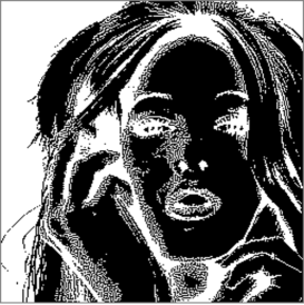
Let us consider the smoothing with binary output template [8]
| (100) |
The initial condition for the state is equal to a given gray-scale image. The boundary condition is given by
| (101) |
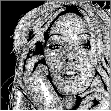
where denotes boundary cells. This template can be used to smooth (average) a gray-scale image and convert into a binary image. It also deletes the noise from the image as shown in Figure 28.
 |
 |
| (a) input image | (b) output image |
 |
 |
| (a) constitutive relation | (b) memductance |
(a) The constitutive relation of the memristor, which is defined by .
(b) Memductance of the memristor, which is defined by . The symbol denotes the unit step function, equal to for and 1 for .
Consider the memristor CNN circuit in Figure 23. Suppose that the flux-controlled memristor has the following constitutive relation and memductance:
| (102) |
and
| (103) |
respectively (see Figure 29). Its terminal voltage satisfies
| (104) |
where
| (105) |
Thus, the terminal voltage satisfies
| (106) |
If becomes zero at , then does not change until for . Compare Eq. (106) with Eq. (77).
Our computer simulations are shown in Figures 30 and 31. We explain their results briefly.
-
1.
The memoristor CNN can not remove the noise from the input image at the initial stage. It is due to the reason that charging flux to memristors can take time, and the memristor can not switch “on” rapidly.
-
2.
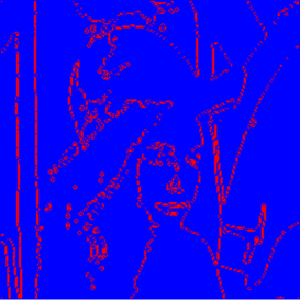
When time is increased, almost memristors change from the “switch-off” state to the “switch-on” state, and the memoristor CNN (65) can delete the noise from the given image by smoothing. It can also hold the output image even if almost memristors switched “off”.
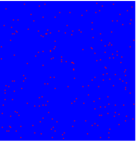
The detailed behavior of the memoristor CNN (65) can be described as follow:
-
1.
All memristors switched “off”. That is, all cells are printed in blue as shown in Figure 30(b). Thus, the memoristor CNN (65) can only convert the given gray-scale image to the binary image. It cannot delete the noise from the image. It is due to the reason that the memoristor CNN (65) cannot respond to the input quickly, since the memristors cannot switch “on” rapidly. -
2.
, , and
Many memristors change to the “switch-on”, and then they switch “off” again, as shown in Figures 30(c), (d), and (e). Note that all memristors do not change between the “switch-off” and ”switch-on” states, synchronously. Furthermore, only the cell with a “switched-on memristor” can smooth (average) the given image, and delete the noise. - 3.
 |
 |
 |
| (a) | (b) | (c) |
 |
 |
 |
| (d) | (e) | (f) |
(a) All memristors switch “off”. Thus, all cells are printed in blue.
(b) All memristors switch “off”, since the memristor can not switch “on” rapidly.
(c) Many memristors is turning from the “switch-off” state (printed in blue) to the “switch-on” state (printed in red).
(d) Most memristos turn to the “switch-on” (printed in red).
(e) Most memristos turn from the “switch-on” state (printed in red) to the “switch-off” state (blue), again.
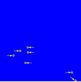
(f) Almost all memristos are switched “off” (printed in blue), except several cells (marked by yellow circles and arrows).
 |
 |
 |
| (a) input gray-scale image () | (b) output image () | (c) output image () |
 |
 |
 |
| (d) output image () | (e) output image () | (f) output image () |
(a) Gray-scale input image for the memoristor CNN (65). All memristors switch “off”.
(b) The memoristor CNN (65) does not delete the noise from the image, since all memristors still switch “off”, that is, the memristor can not switch “on” rapidly.
(c) The memoristor CNN (65) can not delete all noise from the image, though many memristors are turning from the “switch-off” state to the “switch-on” state.
(d) The memoristor CNN (65) deleted the noise from the image, since most memristos turn to the “‘switch-on”.
(e) The memoristor CNN (65) deleted the noise from the image. At this point in time, most memristos turn from the “switch-on” to the “switch-off”, again.
(f) The memoristor CNN (65) can hold a binary output image, even if almost all memristos switched “off”, except for several cells (which is marked by yellow circles and arrows in Figure 30(f)).
8.2 Erosion
Let us consider the erosion template [1, 2]
| (107) |
The initial condition for is given by
| (108) |
and the input is equal to a given binary image. The boundary condition is given by
| (109) |
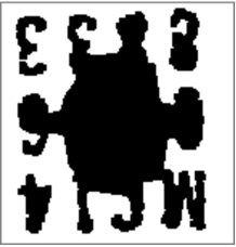
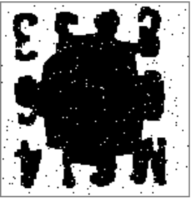
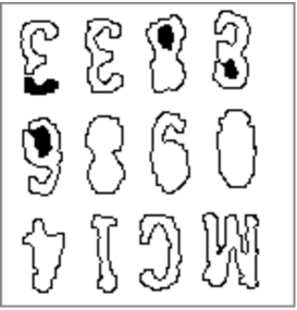
where denotes boundary cells. This template can be used to peel off all boundary pixels of binary image objects, as shown in Figure 32.
 |
 |
| (a) input image | (b) output image |
Consider the memristor CNN circuit in Figure 23. Suppose that the constitutive relation and memductance of the flux-controlled memristor are given by Eqs. (102) and (103), respectively (see Figure 29). Thus, its terminal voltage satisfies
| (110) |
where
| (111) |
For example, if we assume that the inputs satisfy
| (112) |
then we obtain
| (113) |
In this case, we obtain from Eq. (69)
| (114) |
where we assume .
Assume next that the constitutive relation and memductance of the flux-controlled memristor are given by Eqs. (102) and (103), respectively. Then, we obtain
| (115) |
where the input is given by Eq. (112) and . Note that other inputs may satisfy the equation more quickly than the above. That is, all memristors do not switch “on” synchronously, since their terminal flux are not always identical.
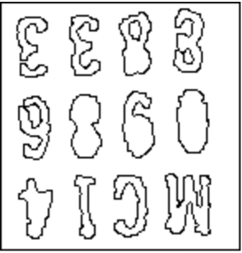
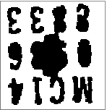
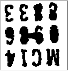
Our computer simulations are shown in Figures 33 and 34.
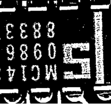
The boundary pixels of the given binary image are peeled off,
and the text becomes clearly visible.
We conclude as follow:
Suppose that the memoristor CNN (65) has the following property: a. The feedback, control, and threshold parameters are given by Eq. (100) or (107). b. The constitutive relation and the memductance of the flux-controlled memristors are given by Eq. (102) and (103), respectively. Then, the memoristor CNN (65) can exhibit the following behavior: 1. The memoristor CNN (65) cannot respond to the input quickly, since the memristors cannot switch “on” rapidly. 2. The memoristor CNN (65) can hold the output image even if almost all memristors switch “off” (refractory period).
 |
 |
 |
| (a) | (b) | (c) |
 |
 |
 |
| (d) | (e) | (f) |
 |
 |
|
| (g) | (h) |
(a) All memristors switch “off”. Thus, all cells are printed in blue.
(b) All memristors switch “off”, since the memristor can not switch “on” rapidly.
(c)-(d) Memristors are turning from the “switch-off” state (printed in blue) to the “switch-on” state (printed in red).
(e) “Switch-on” memristors (printed in red) are turning to the “switch-off” (printed in blue).
(f) “Switch-off” memristors (printed in blue), which do not have switched “on” yet, turn to the “switch-on” state (printed in red).
(g)-(h) All memristos switch “off”, again. Thus, all cells are printed in blue.
 |
 |
 |
| (a) input binary image () | (b) output image () | (c) output image () |
 |
 |
 |
| (d) output image () | (e) output image () | (f) output image () |
 |
 |
|
| (g) output image () | (h) output image () |
(a) Binary input image for the memoristor CNN (65). At this point, all memristors switch “off”. The state is shown in gray.
(b) The memoristor CNN (65) does not peel off the boundary pixels, since all memristors still switch “off”, that is, the memristor can not switch “on” rapidly.
(c)-(e) The boundary pixels are peeled off gradually, since the memristors are turning to the “switch-on” state from the “switch-off” state.
(f) The color of the cells is changed to “black and white” from “gray and white”.
(g)-(h) The memoristor CNN (65) hold the output image, even if all memristos switch “off”, again (see Figure 33(g) and (h))
9 Suspend and Resume Feature
The suspend and resume feature are useful when we want to save the current state, and continue work later from the same state. We show that the memristor CNN has the similar feature.
(1) Parameters: .
(2) The characteristic of the nonlinear resistor (light blue) is given by , where is a constant.
(3) The terminal currents and voltages of the flux-controlled memristor (orange) satisfies . The symbol denotes the unit step function, equal to for and 1 for .
(4) The output voltage of the summing amplifier (pink) is given by .
(5) The above output voltage contains the voltage of the capacitor (the last term).
(6) The above sum does not contain the term ().
(7) The output and the state of each cell are related via the sign function (green): .
Let us consider the memristor CNN in Figure 35. The parameters are given by
| (116) |
The characteristic of the nonlinear resistor is given by
| (117) |
where is a constant. The constitutive relation and memductance of the flux-controlled memristor are given by
| (118) |
and
| (119) |
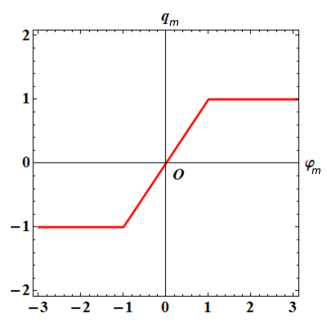
respectively (see Figure 36), where and denote the charge and the flux of the memristor, respectively, the symbol denotes the unit step function, equal to for and 1 for .
 |
 |
| (a) constitutive relation | (b) memductance |
(a) The constitutive relation of the memristor, which is given by .
(b) Memductance of the memristor, which is defined by . Here, the symbol denotes the unit step function, equal to for and 1 for .
(1) Parameters: .
(2) The characteristic of the nonlinear resistor (light blue) is given by , where is a constant.
(3) The terminal currents and voltages of the memristor satisfies .
(4) The output voltage of the summing amplifier is given by .
(5) The above output voltage contains the voltage of the capacitor (the last term).
(6) The above sum does not contain the term , ().
(7) The output voltage of the summing amplifier is equal to .
(8) The output and the state of each cell are related via the sign function (green): .
The memristor CNNs in Figures 35 and 37 work as follows:
- 1.
-
2.
Stored procedure
Turn “on” the switch in Figure 35 during the period from to , where . In this period, the output is connected to the memristor. The stored flux is give by(120) It is recast into the form
(121) which is the time average of the output .
Thus, is regarded as the time average of the output except for a scale factor of . -
3.
Suspend procedure
Power off the memristor CNN in Figure 35 at . Then the computing process is suspended. The ideal memristor can retrieve stored information even after power off, since it is a non-volatile element. If the memristor is not ideal, for example, it has a parasitic capacitance as shown in Figure 38, then after long time power off, the flux of the memristor may decay via a parasitic capacitance [7]. We discuss its effect in Sec. 10.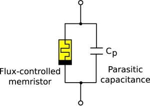
Figure 38: Parasitic capacitance of the flux-conrolled memristor. -
4.
Recovery procedure
In order to continue the process from the previous state, we use the circuit in Figure 37, where we use the memritor in Figure 35.Let us first set the switch to the position at . Then, the current through the cell is given by
(122) where , and is defined by
(123) where and .
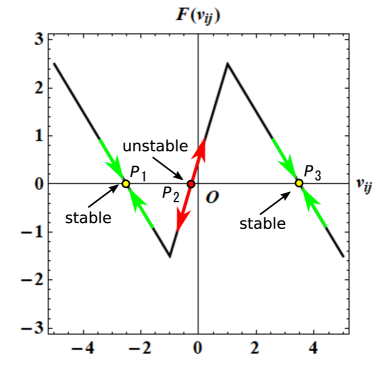
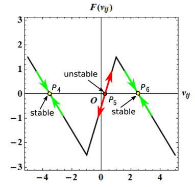
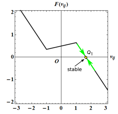
(a) i= 0.5 (b) i = -0.5 Figure 39: Driving-point plot of Eq. (126) with . Equation (126) has two stable equilibrium points (yellow), and one unstable equilibrium points (red). If , then . If , then . Consider next the dynamics of the cell, which is given by
(126) We show the driving-point plot of Eq. (126) in Figure 39. Let us consider the case where . Then, Eq. (126) has two stable equilibrium points, and one unstable equilibrium points as shown in Figure 39. Furthermore, if , then the equilibrium points are given by
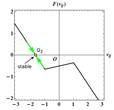
(127) where the points and are stable, and the point is unstable. If , then the equilibrium points are given by
(128) where the points and are stable, and the point is unstable.
The initial condition for Eq. (126) is given by , since the power of the system was turned off during the period of time from to . From the driving-point plot in Figure 39, we obtain
(129) Here, the initial condition is given by .888Note that the power was turned off during the period of time from to . Thus, . Since the solution of Eq. (126) for can not move across the unstable equilibrium point, we obtain
(130) where . Furthermore, from Eqs. (125) and (130), we obtain
(131) where denotes the stored flux during the period from to , and it is the time average of the output except for a scale factor of . We have just recovered the previous average output from .999We did not use , but , where the system is turned off at .
-
5.
Resume procedure
Set the switch to the position . Then, the image processing starts again from the previous average output state. That is, we can resume the computation.
We show next two examples of the suspend and resume feature.
9.1 Hole-filling
Let us consider the hole-filling template [1, 8]
| (132) |
The initial condition for the state is equal , and the input is equal to a given binary image. The boundary condition is given by
| (133) |
where denotes boundary cells. This template can fill the interior of all closed contours in a binary image as shown in Figure 40.
 |
 |
| (a) input image | (b) output image |
We show our detailed computer simulations in Figure 41. Observe that even if we turn off the power of the memristor CNN during the computation, it can resume from the previous average output state.
 |
 |
 |
| (a) | (b) | (c) |
| (input image) | (processing) | (power off) |
 |
 |
 |
| (d) | (e) | (f) |
| (recovered) | (resumed from ) | (processing) |
 |
 |
|
| (g) | (h) | |
| (processing) | (processing) |
(a) Input image (image size is ).
(b) Processing image at . The switch in Figure 35 is closed during the period .
(c) Power off during the period . In this period, the cell output (gray in pseudo-color).
(d) Recovered image at . The previous average output is recovered by setting the switch in Figure 37 to the position . The recovering period is .
(e)-(h) Processed images at time , which are resumed from . In this period, the switch in Figure 37 is set to the position . Observer that the memristor CNN can fill the interior of all closed contours in the binary input image, even if we power off the circuit in the middle of image processing.
9.2 Half-toning
Let us consider the half-toning template [1, 8]
| (134) |
The initial condition for the state is equal to a given gray-scale image, and the input is also equal to a given gray-scale image. The boundary condition is given by
| (135) |
where denotes boundary cells. This template can transform a gray-scale image into a “half-tone” binary image. The binary image preserves the main features of the gray-scale image as shown in Figure 42.
 |
 |
| (a) input image | (b) output image |
 |
 |
| (a) i= 0.5 | (b) i = -0.5 |
Since , Eq. (126) has only one stable equilibrium points as shown in Figure 43. If , then the equilibrium points are given by
| (136) |
If , then the equilibrium points are given by
| (137) |
Thus, we obtain
| (138) |
Here, the initial condition is given by .101010Note that the power was turned off during the period of time from to . Thus, . Since , we obtain
| (139) |
Furthermore, from Eqs. (125) and (130), we obtain
| (140) |
where denote the stored flux during the period from to , and is regarded as the time average of the output . Thus, we obtained the same result as that for (see Eq. (131)).
We show next our detailed computer simulations in Figure 44. Observe that even if we turn off the power of the memristor CNN during the computation, it can resume from the previous average output state. Thus, we obtain the following result:
Assume . Then the memristor CNN has the suspend and resume feature, if we use the circuits in Figures 35 and 37.
 |
 |
 |
| (a) | (b) | (c) |
| (input image) | (processing) | (processing) |
 |
 |
 |
| (d) | (e) | (f) |
| (power off) | (recovered) | (resumed from ) |
 |
 |
 |
| (g) | (h) | (i) |
| (processing) | (processing) | (processing) |
(a) Input image (image size is ).
(b) Processing image at .
(c) Processing image at . Note that the switch in Figure 35 is closed during the period .
(c) Power off during the period . In this period, the cell output (gray in pseudo-color).
(d) Recovered image at . The previous average output is recovered by setting the switch in Figure 37 to the position . The recovering period is .
(f)-(i) Processed images at time , which are resumed from time . In this period, the switch in Figure 37 is set to the position . Observer that the memristor CNN can transform the recovered image into the half-tone binary image, even if we power off the circuit in the middle of image processing.
9.3 Long-term and short-term memories
In our brain’s system, a long-term memory is a storage system for storing and retrieving information. A short-term memory is the short-time storage system that keeps something in mind before transferring it to a long-term memory.
Consider the circuit in Figure 35. Thus, if the switch in Figure 35 is “off”, then the output is hold only when the power is turned on. In this case, the circuit is regarded as a short-term memory circuit. If the switch is “on”, then the time average of the output is stored in the memristor, and we can retrieve it, even if the power is turned off. That is, the ideal memristor can retrieve stored information even after power off, since it is a non-volatile element. In this case, the circuit becomes a long-term memory circuit. Thus, we conclude as follow:
The memristor CNN has functions of the short-term and long-term memories, if we use the circuits in Figure 35.
10 Effect of Flux Decay of Memristors
A certain degree of decay of the flux or the charge is inevitable in physical devices. For example, the flux of the memristor may decay via a parasitic capacitance after long time power off [7].
Let us assume that the flux decays to small value without change of sign. Then, the memductance satisfies
| (141) |
where . The current through the cell in Figure 37 is given by
| (142) |
where . From Eq. (130), we obtain
| (143) |
Thus, the output of the cell does not change even if the flux decays to small value. Note that the output depends on only the sign of , but it does not depend on its value. Thus, we can choose that for the computer simulation.
We show our computer simulations in Figures 45 and 46, where we assume that the flux of the percent of memristors decays to small value without change of sign after power off. Observe that the memristor CNN defined by Figures 35 and 37 works well.
The interesting thing is that if the flux of only the “ percent” of memristors decay to small value with change of sign, then the hole-filling template does not work, as shown in Figure 47. Thus, the suspend and resume feature does not work if the change of sign occurs by memristor failures or parasitic elements. In this case, some error-correcting mechanisms should be used. However, the half-toning template works well even if the flux of “all” memristors decay to small value with change of sign, as shown in Figure 48. In this case, the output image for the half-toning template does not depend on the initial condition. Thus, we conclude as follow:
Assume . Then the memristor CNN defined by Figures 35 and 37 has the suspend and resume feature, even if the flux of the memristors decays to a small (but not too small) value, without change of sign, after power off.
 |
 |
| (a) input image | (b) flux-decayed cell (yellow) |
 |
 |
| (c) recovered image at | (d) output image at |
(a) Input binary image (image size is ).
(b) After power off (during the period ), we assume that the flux of the percent of memristors decays to small value without change of sign by parasitic capacitances. The flux-decayed cells are colored in yellow. Other cells are colored in blue. The cell size is , since the input image size is .
(c) Recovered image at .
(d) Output image at . Observe that the memristor CNN defined by Figures 35 and 37 works well even if the flux of the percent of memristors decays to sufficiently small value.
 |
 |
| (a) input image | (b) flux-decayed cell (yellow) |
 |
 |
| (c) recovered image at | (d) output image at |
(a) Input gray-scale image (image size is ).
(b) After power off at , we assume that the flux of the percent of memristors decays to small value without change of sign by parasitic capacitances. The flux-decayed cells are colored in yellow. Other cells are colored in blue. The cell size is , since the input image size is .
(c) Recovered image at .
(d) Output image at . Observe that the memristor CNN defined by Figures 35 and 37 works well even if the flux of the percent of memristors decays to sufficiently small value.
 |
 |
| (a) input image | (b) flux-decayed cell (red) |
 |
 |
| (c) recovered image at | (d) output image at |
(a) Input binary image (image size is ).
(b) After power off at , we assume that the flux of the percent of memristors decays to small value with change of sign. The flux-decayed cells are colored in red, and the other cells are colored in blue. The cell size is , since the input image size is .
(c) The recovered image at .
(d) Output image at . Observe that if the flux of the percent of memristors decays to small value with change of sign, then the hole-filling template (132) does not work well.
 |
 |
| (a) input image | (b) flux-decayed cell (red) |
 |
 |
| (c) recovered image at | (d) output image at |
(a) Input gray-scale image (image size is ).
(b) After power off at , we assume that the flux of “all” memristors decays to small value with change of sign. The flux-decayed cells are colored in red. In this case, all cells are colored in red. The cell size is , since the input image size is .
(c) Recovered image at .
(d) Output image at . Observe that the half-toning template (134) works well, even if the flux of all memristors decays to sufficiently small value with change of sign.
11 Reset of Memristors
Before a new programming, we should reset the memristor to its zero state. A capacitor can simply be discharged by shorting its terminals (a wire has a negligibly small resistance). However, in order reset the flux of the memristor, we have to supply the reversed input signal, which was used in the previous programming. If the flux-controlled memristor is ideal and passive, then we can reset the memristor to its zero state by connecting a small capacitor to the memristor in parallel [7].
12 Two-dimensional Waves
In this section, we show that the memristor CNN can exhibit interesting two-dimensional waves. Consider the memristor CNN circuit in Fig. 49. We connected the inductor in parallel with the capacitor . In this case, the dynamics of the memristor CNN is given by
Dynamics of the memristor CNN
(144)
where . The terminal currents and voltages of the flux-controlled memristor (yellow) satisfies . Here, the memductance is defined by
| (145) |
where , , , , and are parameters, and the symbol denotes the unit step function, equal to for and 1 for , and .
Let us consider the hole-filling template [1, 8] again
| (146) |
The initial condition for the state and the input are equal to a given binary image. The boundary condition is given by
| (147) |
where denotes boundary cells. If we adjust the parameters , , , and , then the memristor CNN (144) can exhibit many interesting two-dimensional waves, as shown in Fig. 50.
(1) Parameters: .
(2) The characteristic of the nonlinear resistor (light blue) is given by , where is a constant.
(3) The terminal currents and voltages of the flux-controlled memristor (yellow) satisfies , where is the memductance defined by Eq. (refleqn: wave-W).
(4) The output voltage of the summing amplifier (pink) is given by .
(5) The above output voltage contains the voltage of the capacitor (the last term).
(6) The above sum does not contain the term ().
(7) The output and the state of each cell are related via the sign function (green): .
 |
 |
 |
| (a) input image | (b) | (c) |
 |
 |
 |
| (d) | (e) | (f) |
 |
 |
 |
| (g) | (h) | (i) |
13 Conclusion
We have shown that the flux-controlled memristors cannot respond to the sinusoidal voltage source quickly. Furthermore, these memristors have the refractory period after switch “on”. We have shown that the memristor-coupled two-cell CNN can exhibit chaotic behavior. We have also proposed the memristor CNN, which can hold the output image, even if even if all cells are disconnected and no signal is supplied to the cell after a certain point of time, by memristor’s switching behavior. We have next shown that even if we turn off the power of the memristor CNN during the computation, it can resume from the previous average output state. That is, the memristor CNN has the suspend and resume feature. Furthermore, the memristor CNN has functions of the short-term and long-term memories. Finally, we have shown that the memristor CNN can exhibit the interesting two-dimensional waves, if an inductor is connected to each memristor CNN cell. In this paper, we used the Euler method for solving the differential equations. In order to get more accurate results, we may need high accuracy numerical methods, for example, the Runge-Kutta method.
References
- [1] Chua, L. O. (1998) CNN: A Paradigm for Complexity (World Scientific, Singapore).
- [2] Chua, L. O. and Roska, T. (2002) Cellular neural networks and visual computing (Cambridge University Press, Cambridge), 2002.
- [3] Itoh, M. and Chua, L.O. (2003) Designing CNN genes. Int. J. Bifurcation and Chaos, 13(10), 2739-2824.
- [4] Itoh, M. and Chua, L.O. (2009) Memristor cellular automata and memristor discrete-time cellular neural networks. Int. J. Bifurcation and Chaos, 19(11), 3605-3656.
- [5] Chua, L. O. (1971) Memristor–The missing circuit element. IEEE Transactions on Circuit Theory, CT-18 (5), 507-519.
- [6] Chua, L. O. and Kang, S. M. (1976) Memristive devices and systems. Proc. IEEE, 64(2), 209-223.
- [7] Itoh M. and Chua L. O. (2016) Parasitic effects on memristor dynamics. Int. J. Bifurcation and Chaos, 26(6), 1630014-1-55.
- [8] Roska,T., Kék, L., Nemes, L., and Zarándy, Á. (1997) CNN software library (templates and algorithms). version 7.0 (DNS-1-1997). Analogical and Neural Computing Laboratory, Computer Automation Institute, Hungarian Academy of Sciences, Budapest, Hungary.