Quantum-dot-like states in molybdenum disulfide nanostructures due to the interplay of local surface wrinkling, strain, and dielectric confinement
Abstract
The observation of quantum light emission from atomically thin transition metal dichalcogenides has opened a new field of applications for these material systems. The corresponding excited charge-carrier localization has been linked to defects and strain, while open questions remain regarding the microscopic origin. We demonstrate that the bending rigidity of these materials leads to wrinkling of the two-dimensional layer. The resulting strain field facilitates strong carrier localization due to its pronounced influence on the band gap. Additionally, we consider charge carrier confinement due to local changes of the dielectric environment and show that both effects contribute to modified electronic states and optical properties. The interplay of surface wrinkling, strain-induced confinement, and local changes of the dielectric environment is demonstrated for the example of nanobubbles that form when monolayers are deposited on substrates or other two-dimensional materials.
In the past, single-photon emission has been realized using trapped-ion systems ion , NV centers in diamond PhysRevLett.100.077401 , and epitaxially grown quantum dots QD with important applications in quantum information. Recently, single-photon emission from spatially localized centers in transition metal dichalcogenides (TMDs) has been demonstrated srivastava_optically_2015 ; koperski_single_2015 ; chakraborty_voltage-controlled_2015 ; he_single_2015 ; kern_nanoscale_2016 ; branny_discrete_2016 ; kumar_strain-induced_2015 ; branny_deterministic_2017 ; palacios-berraquero_large-scale_2017 ; khestanova_universal_2016 ; shepard_nanobubble_2017 . For this purpose, TMD monolayers have been placed over gold nanostructures kern_nanoscale_2016 ; branny_discrete_2016 , substrates with etched holes kumar_strain-induced_2015 , and arrays of dielectric micropillars branny_deterministic_2017 ; palacios-berraquero_large-scale_2017 . In the latter case, up to 96% active single-photon emitters have been obtained. Quantum light emission has been also achieved with nanobubbles, which are formed in vertically stacked TMD structures khestanova_universal_2016 ; shepard_nanobubble_2017 .
Single-photon emission from atomically thin TMDs can originate either from structural defects resulting in electronic trap states, which are known to be a source of photoluminescence centers Tongay:13 ; ChowP:15 , or due to strain-induced potentials with three-dimensional carrier confinements. In this paper, we show that the strain-induced occurrence of localized electronic states is intrinsically linked to a non-continuous deformation of the TMD surface. We find that bending of the atomically thin sheet leads to formation of local surface wrinkles and bond deformations are identified as their microscopic origin. Due to the strong dependence of the TMD band gap on local strain fields Steinhoff:14 this wrinkling induces a spatially localized carrier confinement. We show that this wrinkling takes place on length scales of nm, providing efficient three-dimensional localized states and thereby enabling single-photon emission. This supports recent experimental results branny_discrete_2016 , which first established the connection between surface wrinkling and localized emission, although the resolution of the used confocal microscopy is limited to much larger m length scales. The local wrinkling effect is different from surface corrugations on a nm scale, that is known for many 2D materials, as studied for graphene in Ref. Meyer:07 .
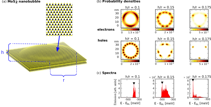
To investigate the interplay between TMD layer deformations and carrier confinement, we model a TMD layer with atomic resolution using a million-atom supercell. Based on valence force field simulations, new equilibrium positions of the individual atoms in the bended material are determined. The information about the displaced atoms is used in a tight-binding electronic-state calculation for the supercell structure. For the example of nanobubbles, we demonstrate that surface wrinkling acts as the main cause for quantum confinement with quantum-dot-like electronic states. The considered geometry is depicted in Fig. 1(a). Nanobubbles are formed when placing a monolayer of MoS2 on another MoS2 sheet used as a flat substrate, which is comparable to recent experimental investigations khestanova_universal_2016 . Starting from a paraboloid profile of the nanobubble, the relaxation of atoms in the upper TMD layer is performed while keeping the atoms in the lower layer fixed. For this part, we utilize a REAX potential ReaxFF with the parametrization from Ref. ostadhossein_reaxff_2017 within a valence force field calculation, which is capable of accurately describing bond deformations under strain as well as continuous bond formation and breaking dynamics. We find that both in-plane strain and bending contribute to the shape of the nanobubble (see Supporting Information for more details). Subsequent electronic-state calculations use this information about the positions of the individual atoms. For a supercell with an in-plane extension of 130 nm and up to 1.2 atoms, a 6-band tight-binding Hamiltonian is solved using the parametrization given in the Supporting Information. Strain-induced local band gap changes arising from the displaced atomic positions are included via a generalized Harrison rule froyen_elementary_1979 . Additionally, when locally detaching the upper layer from the substrate underneath and changing from a commensurate bilayer to monolayer-like structures across the nanobubble, a modified dielectric environment and electronic hybridization is expected cheiwchanchamnangij_quasiparticle_2012 ; rosner_two-dimensional_2016 ; raja_coulomb_2017 ; dielectric_nanoletter_florian . We include both effects into our model by changing individual tight-binding parameters based on GW calculations, as explained in the Supporting Information. Based on the calculated tight-binding states, optical emission spectra are obtained using Fermi’s golden rule.
In our analysis, we consider nanobubbles of different aspect ratios and sizes. The degree of localization is controlled by the aspect ratio, as shown in Fig. 1(b). In contrast, the nanobubble size does not change the qualitative behavior, as presented in the appendix. For the single-particle states are delocalized along the edge of the bubble, whereas for an increasing aspect ratio of distinct maxima are found. Due to the increased strain, these maxima carry the symmetry of the underlying crystal lattice. The trend of stronger localization with increasing aspect ratio continues for , which corresponds to the experimentally reported value of Ref khestanova_universal_2016 . In this case, the probability densities are localized at three distinct positions at the edge of the nanobubble.
Figure 1(c) provides the emission spectra corresponding to the three different aspect ratios in Fig. 1(b), obtained from all confined states of the TB model and Fermi’s golden rule. For , the oscillator strength is very weak due to a small dipole interaction matrix element, which is the result of a much larger radial broadening of the probability density for the electrons than for the holes. More optical transitions are present for larger aspect ratios . In the case of strong emission from the electron and hole states, shown in the right panel of Fig. 1(b), as well as a broad background emission from other states is obtained. A similar behavior has been observed in recent experiments with WSe2 nanobubbles shepard_nanobubble_2017 and can be explained by increasing strain, which leads to a deeper confinement, stronger localization of the single-particle states, as seen in Fig. 1(b), and a redshift of the optical spectra.
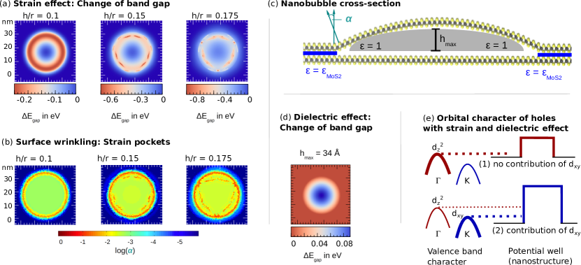
To analyze the mechanism behind the strong carrier localization, we quantify the contributions to the confinement potential due to strain as well as local changes of the screening and electronic hybridization for the upper TMD layer. As a result of the nanobubble geometry, shown in Fig. 2(c), the dielectric and electronic environment outside of the bubble corresponds to a bilayer, while, in the center of the bubble, the large distance between top and bottom layer resembles the situation of a monolayer. This effect increases with increasing height of the bubble, as illustrated in Fig. 2(c). The resulting changes of band gap are depicted in Fig. 2(d). Effectively, it leads to a repulsive potential in the center of the bubble. From our calculations we obtain band gap changes on the order of meV, consistent with recent measurements raja_coulomb_2017 .
The strain-induced changes of band gap for three different aspect ratios are displayed in Fig. 2(a). By comparing these strain effects with the probability densities in Fig. 1(b), we can conclude that the strain-induced changes of the band gap are responsible for the increasing localization, as the dielectric effect is rotationally symmetric (see Fig. 2(d)). For aspect ratios of and , strain pockets are found. To illuminate their origin, the average angle between normal vectors at neighboring unit cells (schematically depicted in Fig. 2(c)) is displayed in Fig. 2(b), as described by the normal-normal correlation function (see Supporting Information). These average angles reveal a local wrinkling of the surface for aspect ratios of and , with the angle of the normal vectors between neighboring unit cell varying up to . A comparison between Figs. 2(a) and (b) shows that the strain becomes non-uniform and peaks in the wrinkles. The physical origin of this behavior can be traced back to the high Young’s modulus of MoS2 (see e.g. Ref. ostadhossein_reaxff_2017 ; TMD-mechanics ). The higher the modulus, the better a material resists against compression/elongation. Especially for a high modulus, the material tends to minimize its total change of length. In particular, this is possible by the formation of wrinkles. The bond deformations responsible for the wrinkling are more prominent in TMDs than in graphene, as the former consist of a tri-atomic structure, in which the transition metal atoms are sandwiched between chalcogen atoms. Additionally, the spherical deformation of the material that is imposed by the nanobubble geometry favors wrinkle formation. We expect the wrinkles to be a general feature of spherical deformations, in contrast to depositing the material on a cylindrical surface or over a ridge. Mathematically, the difference between these situations lies in the Gaussian curvature Nakahara of the geometry that is imposed upon the TMD monolayer. The strong band gap variations, induced by strain and the dielectric environment, also influence the oscillator strength of the optical transitions in Fig. 1(c). The main reason for this change is illustrated in Fig. 2(e). The localized electron states, originating from the conduction band, inherit the orbital character of the -point. In the strained bubble geometry, the valley lies energetically higher than the -valley for holes. Depending on the depth of the confinement potential, the orbital character of the localized hole states is than either determined by states originating from the -point (), or from both the - and the -point (). In the former case, the emission is weak, as the electron and hole wave functions carry the same orbital character (). In the latter case, the strong dipole matrix element of the -point transition dominates, as known from the 2D monolayer Steinhoff:14 . These large differences in the dipole matrix elements explain why the measured recombination times of a few nanoseconds srivastava_optically_2015 ; shepard_nanobubble_2017 for localized states in TMD nanostructures are much longer than the sub-picosecond range, which is observed for the 2D monolayer poellmann_radiative_decay2015 .
In summary, our calculations provide insight into the mechanism of quantum-dot-like carrier localization in TMD nanostructures for the example of MoS2 nanobubbles. We find a strong localization on the nanometer scale inside strain pockets, which carry the symmetry of the underlying crystal lattice. It is demonstrated that the formation of such strain pockets is caused by a non-uniform strain, which peaks in surface wrinkles, an effect that is inaccessible to continuum theory. Our method is based on the requirements of covering strain as well as local changes of the screening and electronic hybridization on the nanometer scale. We quantify the contributions of these effects to the confinement potential in a combined atomistic valence force-field and million-atom supercell tight-binding approach. Regarding the emission properties, it is shown that the orbital character of the localized states changes compared to the 2D monolayer, explaining the measured recombination times of a few nanoseconds srivastava_optically_2015 ; shepard_nanobubble_2017 in TMD nanostructures. We expect these properties and mechanisms to be present in other TMD nanostructures, since the underlying physical properties are universal for TMD materials. Our results are expected to stimulate new and alternative realizations of strong carrier confinement in atomically thin TMD semiconductors.
Acknowledgements
The authors gratefully acknowledge computational resources from HLRN Berlin and funding from the DFG (”Deutsche Forschungsgemeinschaft”) via the graduate school ”Quantum-Mechanical Material Modeling”.
*
Appendix A Nanobubble geometry
Starting point of our relaxation procedure is a rectangular supercell of a MoS2 bilayer with periodic boundary conditions and an interlayer equilibrium distance of in accordance with Ref. ostadhossein_reaxff_2017 . The top layer, which subsequently forms the bubble, is shorter in both lateral directions so that its atoms are not influenced by the boundary conditions. To generate the bubble, the atoms of the top layer are displaced onto a paraboloid with a given height, corresponding to the desired aspect ratio.
In order to determine the relaxed atomic positions, we employ the LAMMPS code plimpton_fast_1995 using the REAX potential of Ref. ostadhossein_reaxff_2017 . To achieve a convergent geometry, we utilize a supercell of dimensions nmnmnm, containing about atoms. The relaxation is performed until a force tolerance of or a relative energy tolerance of is reached. In each iteration step, the charge equilibration energy is minimized until it reaches a value below eV.
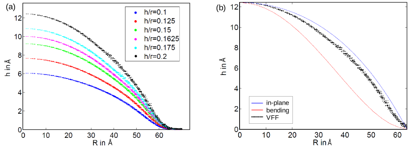
The obtained atomic positions provide access to height profiles of MoS2 bubbles for different aspect ratios , which are depicted in Fig. 3(a). In Fig. 3(b), these values are compared to continuum elasticity theory khestanova_universal_2016 , where two cases, dominated by in-plane strain and bending, can be distinguished. Since our microscopically calculated height profile of the bubble is in between these limits, we conclude that both aspects contribute.
A.1 Monolayer tight-binding model
To describe the TMD monolayer, we employ an effective TB Hamiltonian with nearest and next-nearest neighbor interactions between Mo atoms and a basis set. The respective Hamilton matrix in -space is given by
| (1) |
with matrix elements
| (2) |
For the atomic positions , we consider nearest neighbors and next nearest neighbors , using the in-plane coordinates
| (3) |
in units of the the Bravais-lattice vectors
| (4) |
with the lattice constant . The matrix elements
| (5) |
include the TB hopping parameter towards nearest and next-nearest neighbors of the Mo-atoms, respectively.
| -2.17187 eV | |
| -2.07972 eV | |
| -0.326583 eV | |
| 0.561734 eV | |
| -0.411327 eV | |
| -0.355268 eV | |
| -0.0537226 eV | |
| -0.00459159 eV | |
| 0.052774 eV | |
| -0.123627 eV |
While the threefold symmetry of the MoS2 lattice would be enhanced to a six-fold symmetry when considering the Mo sublattice only, we retain the original C3v symmetry by including different phase factors towards nearest and next-nearest neighbours
| (6) |
Following Ref. PhysRevB.88.085433 , we include spin-orbit coupling according to
| (9) |
with
| (13) |
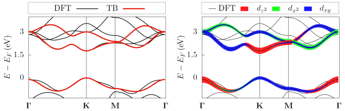
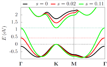
The Hamiltonian in Eq. (9) is block diagonal, which means that the -component of the spin is not mixed by the spin-orbit coupling and serves as a good quantum number due to the symmetry PhysRevB.88.085433 . By using our TB approach, the band structure of DFT calculations is well approximated, as shown in Fig. 4. The DFT calculations were performed using the VASP code Kresse1 ; Kresse2 together with the supplied projector augmented wave (PAW) potentials Kresse3 and a 16 x 16 x 1 -point sampling of the Brillouin zone. The used TB parameters for a MoS2 monolayer are given in Table. 1.
Hamiltonian at points of high symmetry
Both strain and changes of the dielectric environment influence the band gap of MoS2. To incorporate these effects into the TB model, we diagonalize the TB Hamiltonian analytically at points of high symmetry, which allows for an identification of the TB parameters to be adapted. For the -point we find
| (14) |
with the first diagonal element, denoting the eigenvalue of the valence band (VB) and the other two, describing the conduction bands (CBs). At the -point, we obtain
| (15) |
In the next section, we discuss how these results can be used to incorporate the effects of strain and of the dielectric environment into the TB Hamiltonian.
A.2 Tight-binding model for nanobubbles
Implementation of strain
In the case of a MoS2 monolayer, strain leads to an transition between a direct band gap at the -point and an indirect band gap between the -point of the VB and the -point of the CB, as demonstrated for instance in Ref. PhysRevB.87.235434 . From Eqs. (14) and (15), we obtain
| (16) |
Hence, we can modify the nearest neighbor hopping parameter to describe the direct to indirect transition in strained monolayers. We employ a generalized Harrison rule froyen_elementary_1979
| (17) |
with , where is the inter-atomic distance and the lattice constant. For an exponent of the experimental band gaps in Ref. conley_bandgap_2013 are reproduced. The band structure for different strain situations within this approach is depicted in Fig. 5.
Implementation of the dielectric environment
In addition to strain, the band gap can also be modified by changing the dielectric environment of the layer rosner_two-dimensional_2016 ; raja_coulomb_2017 . While the system resembles a monolayer in the middle of the bubble, it corresponds to a bilayer at the edges. In this transition, not only the value of the band gap changes, but also its character. ARPES measurements PhysRevLett.111.106801 demonstrate that the MoS2 monolayer band gap is direct, whereas the bilayer band gap is indirect. Additionally, the value of the band-gap at the -point is reduced, due to more efficient dielectric screening. To determine this band gap as a function of the interlayer distance , we use data from DFT+GW calculations Steinhoff:14 ; cheiwchanchamnangij_quasiparticle_2012 . Assuming a bowing-like behavior for the change of band gap with interlayer distance, a quadratic interpolation leads to
| (18) |
for the direct band gap at the -point.
To introduce the influence of the air gap between the surface and bottom layer within the nanobubble into the TB Hamiltonian, we follow the same route as in the previous section and determine the hopping parameter as a function of . Thereby, the parameter in our TB model depends on the interlayer distance according to.
| (19) |
A.3 Normal-normal correlation
To investigate the wrinkling of the material, we determine the normal-normal correlation function
| (20) |
that measures the angle between the normal vectors of neighboring unit cells. Due to the symmetry of the system, each cell has three neighboring cells , which gives rise to the normalization in equation (20). For better visibility in Fig. 2b we depict the average angle between adjacent normal vectors .
A.4 Influence of nanobubble size
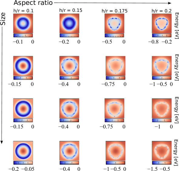
In Fig. 6 we show the influence of both size and aspect ratio variations on the effective confinement potential for the nano-bubble. We find that the trend towards stronger localization is controlled by the aspect ratio, while the size of the bubble controls the depth of the confinement potential and the distinctness of the observed localization.
References
- (1) D B Higginbottom, L Slodička, G Araneda, L Lachman, R Filip, M Hennrich, and R Blatt. Pure single photons from a trapped atom source. New Journal of Physics, 18(9):093038, 2016.
- (2) A. Batalov, C. Zierl, T. Gaebel, P. Neumann, I.-Y. Chan, G. Balasubramanian, P. R. Hemmer, F. Jelezko, and J. Wrachtrup. Temporal coherence of photons emitted by single nitrogen-vacancy defect centers in diamond using optical rabi-oscillations. Phys. Rev. Lett., 100:077401, Feb 2008.
- (3) Pascale Senellart, Glenn Solomon, and Andrew White. High-performance semiconductor quantum-dot single-photon sources. Nature Nanotechnology, 12, Nov 2017.
- (4) Ajit Srivastava, Meinrad Sidler, Adrien V. Allain, Dominik S. Lembke, Andras Kis, and A. Imamoğlu. Optically active quantum dots in monolayer WSe2. Nat Nano, 10(6):491–496, 2015.
- (5) M. Koperski, K. Nogajewski, A. Arora, V. Cherkez, P. Mallet, J.-Y. Veuillen, J. Marcus, P. Kossacki, and M. Potemski. Single photon emitters in exfoliated WSe2 structures. Nat Nano, 10(6):503–506, 2015.
- (6) Chitraleema Chakraborty, Laura Kinnischtzke, Kenneth M. Goodfellow, Ryan Beams, and A. Nick Vamivakas. Voltage-controlled quantum light from an atomically thin semiconductor. Nat Nano, 10(6):507–511.
- (7) Yu-Ming He, Genevieve Clark, John R. Schaibley, Yu He, Ming-Cheng Chen, Yu-Jia Wei, Xing Ding, Qiang Zhang, Wang Yao, Xiaodong Xu, Chao-Yang Lu, and Jian-Wei Pan. Single quantum emitters in monolayer semiconductors. Nat Nano, 10(6):497–502.
- (8) Johannes Kern, Iris Niehues, Philipp Tonndorf, Robert Schmidt, Daniel Wigger, Robert Schneider, Torsten Stiehm, Steffen Michaelis de Vasconcellos, Doris E. Reiter, Tilmann Kuhn, and Rudolf Bratschitsch. Nanoscale positioning of single-photon emitters in atomically thin WSe2. Adv. Mater., 28(33):7101–7105, 2016.
- (9) Artur Branny, Gang Wang, Santosh Kumar, Cedric Robert, Benjamin Lassagne, Xavier Marie, Brian D. Gerardot, and Bernhard Urbaszek. Discrete quantum dot like emitters in monolayer MoSe2: Spatial mapping, magneto-optics, and charge tuning. Appl. Phys. Lett., 108(14):142101, 2016.
- (10) S. Kumar, A. Kaczmarczyk, and B. D. Gerardot. Strain-induced spatial and spectral isolation of quantum emitters in mono- and bilayer WSe2. Nano Lett., 15(11):7567–7573, 2015.
- (11) Artur Branny, Santosh Kumar, Raphaël Proux, and Brian D. Gerardot. Deterministic strain-induced arrays of quantum emitters in a two-dimensional semiconductor. Nature Communications, 8:ncomms15053, 2017.
- (12) Carmen Palacios-Berraquero, Dhiren M. Kara, Alejandro R.-P. Montblanch, Matteo Barbone, Pawel Latawiec, Duhee Yoon, Anna K. Ott, Marko Loncar, Andrea C. Ferrari, and Mete Atatüre. Large-scale quantum-emitter arrays in atomically thin semiconductors. Nature Communications, 8:ncomms15093, 2017.
- (13) E. Khestanova, F. Guinea, L. Fumagalli, A. K. Geim, and I. V. Grigorieva. Universal shape and pressure inside bubbles appearing in van der waals heterostructures. Nature Communications, 7:ncomms12587, 2016.
- (14) Gabriella D. Shepard, Obafunso A. Ajayi, Xiangzhi Li, X.-Y. Zhu, James Hone, and Stefan Strauf. Nanobubble induced formation of quantum emitters in monolayer semiconductors. 2D Mater., 4(2):021019, 2017.
- (15) Sefaattin Tongay, Joonki Suh, Can Ataca, Wen Fan, Alexander Luce, Jeong Seuk Kang, Jonathan Liu, Changhyun Ko, Rajamani Raghunathanan, Jian Zhou, Frank Ogletree, Jingbo Li, Jeffrey C. Grossman, and Junqiao Wu. Defects activated photoluminescence in two-dimensional semiconductors: interplay between bound, charged, and free excitons. Scientific Reports, 3:2657, 2013.
- (16) Philippe K. Chow, Robin B. Jacobs-Gedrim, Jian Gao, Toh-Ming Lu, Bin Yu, Humberto Terrones, and Nikhil Koratkar. Defect-induced photoluminescence in monolayer semiconducting transition metal dichalcogenides. ACS Nano, 9(2):1520–1527, 2015. PMID: 25603228.
- (17) A. Steinhoff, M. Rösner, F. Jahnke, T. O. Wehling, and C. Gies. Influence of excited carriers on the optical and electronic properties of mos2. Nano Letters, 14(7):3743–3748, 2014. PMID: 24956358.
- (18) Jannik C. Meyer, A. K. Geim, K. S. Novoselov, and T. J. Booth. The structure of suspended graphene sheets. Nature, 446:60, 2007.
- (19) Adri C. T. van Duin, Siddharth Dasgupta, Francois Lorant, and William A. Goddard. Reaxff. a reactive force field for hydrocarbons. The Journal of Physical Chemistry A, 105(41):9396–9409, 2001.
- (20) Alireza Ostadhossein, Ali Rahnamoun, Yuanxi Wang, Peng Zhao, Sulin Zhang, Vincent H. Crespi, and Adri C. T. van Duin. ReaxFF reactive force-field study of molybdenum disulfide (MoS2). J. Phys. Chem. Lett., 8(3):631–640, 2017.
- (21) Sverre Froyen and Walter A. Harrison. Elementary prediction of linear combination of atomic orbitals matrix elements. Phys. Rev. B, 20(6):2420–2422, 1979.
- (22) Tawinan Cheiwchanchamnangij and Walter R. L. Lambrecht. Quasiparticle band structure calculation of monolayer, bilayer, and bulk mos2. Phys. Rev. B, 85(20):205302, 2012.
- (23) M. Rösner, C. Steinke, M. Lorke, C. Gies, F. Jahnke, and T. O. Wehling. Two-dimensional heterojunctions from nonlocal manipulations of the interactions. Nano Lett., 16(4):2322–2327, 2016.
- (24) Archana Raja, Andrey Chaves, Jaeeun Yu, Ghidewon Arefe, Heather M. Hill, Albert F. Rigosi, Timothy C. Berkelbach, Philipp Nagler, Christian Schüller, Tobias Korn, Colin Nuckolls, James Hone, Louis E. Brus, Tony F. Heinz, David R. Reichman, and Alexey Chernikov. Coulomb engineering of the bandgap and excitons in two-dimensional materials. Nature Communications, 8:15251, 2017.
- (25) Matthias Florian, Malte Hartmann, Alexander Steinhoff, Julian Klein, Alexander W. Holleitner, Jonathan J. Finley, Tim O. Wehling, Michael Kaniber, and Christopher Gies. The dielectric impact of layer distances on exciton and trion binding energies in van der waals heterostructures. Nano Letters, 18(4):2725–2732, 2018.
- (26) Deji Akinwande, Christopher J. Brennan, J. Scott Bunch, Philip Egberts, Jonathan R. Felts, Huajian Gao, Rui Huang, Joon-Seok Kim, Teng Li, Yao Li, Kenneth M. Liechti, Nanshu Lu, Harold S. Park, Evan J. Reed, Peng Wang, Boris I. Yakobson, Teng Zhang, Yong-Wei Zhang, Yao Zhou, and Yong Zhu. A review on mechanics and mechanical properties of 2d materials—graphene and beyond. Extreme Mechanics Letters, 13:42 – 77, 2017.
- (27) M. Nakahara. Geometry, Topology and Physics. CRC Press, 2017.
- (28) C. Poellmann, P. Steinleitner, U. Leierseder, P. Nagler, G. Plechinger, M. Porer, R. Bratschitsch, C. Schüller, T. Korn, and R. Huber. Resonant internal quantum transitions and femtosecond radiative decay of excitons in monolayer wse2. Nature Materials, 14, 2015.
- (29) Steve Plimpton. Fast parallel algorithms for short-range molecular dynamics. Journal of Computational Physics, 117(1):1–19, 1995.
- (30) Gui-Bin Liu, Wen-Yu Shan, Yugui Yao, Wang Yao, and Di Xiao. Three-band tight-binding model for monolayers of group-vib transition metal dichalcogenides. Phys. Rev. B, 88:085433, Aug 2013.
- (31) G. Kresse and J. Hafner. Ab initio. Phys. Rev. B, 47:558–561, Jan 1993.
- (32) G. Kresse and J. Furthmüller. Efficiency of ab-initio total energy calculations for metals and semiconductors using a plane-wave basis set. Computational Materials Science, 6(1):15 – 50, 1996.
- (33) G. Kresse and D. Joubert. From ultrasoft pseudopotentials to the projector augmented-wave method. Phys. Rev. B, 59:1758–1775, Jan 1999.
- (34) M. Ghorbani-Asl, S. Borini, A. Kuc, and T. Heine. Strain-dependent modulation of conductivity in single-layer transition-metal dichalcogenides. Phys. Rev. B, 87:235434, Jun 2013.
- (35) Hiram J. Conley, Bin Wang, Jed I. Ziegler, Richard F. Haglund, Sokrates T. Pantelides, and Kirill I. Bolotin. Bandgap engineering of strained monolayer and bilayer MoS2. Nano Lett., 13(8):3626–3630, 2013.
- (36) Wencan Jin, Po-Chun Yeh, Nader Zaki, Datong Zhang, Jerzy T. Sadowski, Abdullah Al-Mahboob, Arend M. van der Zande, Daniel A. Chenet, Jerry I. Dadap, Irving P. Herman, Peter Sutter, James Hone, and Richard M. Osgood. Direct measurement of the thickness-dependent electronic band structure of using angle-resolved photoemission spectroscopy. Phys. Rev. Lett., 111:106801, Sep 2013.