Electronic band structure of ultimately thin silicon oxide on Ru(0001)
Abstract
Silicon oxide can be formed in a crystalline form, when prepared on a metallic substrate. It is a candidate support catalyst and possibly the ultimately-thin version of a dielectric host material for two-dimensional materials (2D) and heterostructures. We determine the atomic structure and chemical bonding of the ultimately thin version of the oxide, epitaxially grown on Ru(0001). In particular, we establish the existence of two sub-lattices defined by metal-oxygen-silicon bridges involving inequivalent substrate sites. We further discover four electronic bands below Fermi level, at high binding energies, two of them forming a Dirac cone at K point, and two others forming semi-flat bands. While the latter two correspond to hybridized states between the oxide and the metal, the former relate to the topmost silicon-oxygen plane, which is not directly coupled to the substrate. Our analysis is based on high resolution X-ray photoelectron spectroscopy, angle-resolved photoemission spectroscopy, scanning tunneling microscopy, and density functional theory calculations.
keywords:
ultrathin silicon oxide film, monolayer, photoemission spectroscopy, density functional theory calculations, metal-oxide interfaceIJL] Institut Jean Lamour, UMR 7198, CNRS-Université de Lorraine, Campus ARTEM, 2 allée André Guinier, BP 50840, 54011 Nancy, France CEA] Laboratoire de simulation atomistique, Univ. Grenoble Alpes & CEA 38054 Grenoble France NEEL] Univ. Grenoble Alpes, CNRS, Grenoble INP, Institut Néel, 38000 Grenoble, France IJL] Institut Jean Lamour, UMR 7198, CNRS-Université de Lorraine, Campus ARTEM, 2 allée André Guinier, BP 50840, 54011 Nancy, France MADRID]Departamento de Física Teórica de la Materia Condensada and Condensed Matter Physics Center (IFIMAC), Facultad de Ciencias, Universidad Autónoma de Madrid, E-28049 Madrid, Spain IJL] Institut Jean Lamour, UMR 7198, CNRS-Université de Lorraine, Campus ARTEM, 2 allée André Guinier, BP 50840, 54011 Nancy, France IJL] Institut Jean Lamour, UMR 7198, CNRS-Université de Lorraine, Campus ARTEM, 2 allée André Guinier, BP 50840, 54011 Nancy, France IJL] Institut Jean Lamour, UMR 7198, CNRS-Université de Lorraine, Campus ARTEM, 2 allée André Guinier, BP 50840, 54011 Nancy, France SOLEIL] Synchrotron SOLEIL, Saint-Aubin, BP 48, F-91192 Gif-sur-Yvette Cedex, France SOLEIL] Synchrotron SOLEIL, Saint-Aubin, BP 48, F-91192 Gif-sur-Yvette Cedex, France SOLEIL] Synchrotron SOLEIL, Saint-Aubin, BP 48, F-91192 Gif-sur-Yvette Cedex, France CEA SPEC] SPEC, CEA, CNRS, Université Paris-Saclay, CEA Saclay, 91191 Gif-sur-Yvette Cedex, France NEEL] Univ. Grenoble Alpes, CNRS, Grenoble INP, Institut Néel, 38000 Grenoble, France CEA] Laboratoire de simulation atomistique, Univ. Grenoble Alpes & CEA 38054 Grenoble France IJL] Institut Jean Lamour, UMR 7198, CNRS-Université de Lorraine, Campus ARTEM, 2 allée André Guinier, BP 50840, 54011 Nancy, France
Introduction
Ultrathin oxide films are of paramount technological importance in diverse fields such as catalysis or energy conversion 1, 2, 3, 4. Moreover, the continued trend towards miniaturization of modern micro- and nano-electronics has been driven significant effort in the elaboration of very-high-quality crystalline oxide films down to the ultimate thickness of a single atom or polyhedron. At this (2D) limit, chemical and physical properties such as energy band gap 5, reactivity or flexibility can be profoundly altered. As interestingly as the oxide itself, the interface with the support can exhibit unprecedented electronic properties.
Recently, metal-supported crystalline silicon oxide films have been grown as thin as mono- and bilayers 6, 7, 8, 9, 10, 11, 12, 13, 14, 15, 16, 17, 18, 19, 20, 21, 22, 23, 24, 25, 26, 27, 28, 29, 30, 31. The silicon oxide structure can be described as a network of corner–sharing SiO4 tetrahedra forming a honeycomb lattice. This ultimately thin silicate, also called 2D silicon oxide, has remarkable properties. To date, both in its monolayer (ML) and bilayer (BL) form, it exhibits the largest band gap accessible (about 6.5 eV) among 2D materials making it the ideal 2D insulator 16. Mechanical transfer from the growth substrate to a new support has been recently achieved 32. Therefore, this material can be envisaged to be used as a stacking brick in Van der Waals heterostructures. Like graphene, its properties can be modified by doping33, 34, 31, intercalation35, 36, 37, 38, and creation of defects39, 40.
Finally, it is also an ideal plateform to investigate the amorphous-crystalline phase transformations in 2D 15, 39, 41, a rising research field fuelled by the prospect for applications based on switchable properties.
The structure of ML and BL 2D silicon oxide grown by epitaxy on the surface of metals has been experimentally and theoretically characterized in the case of Mo(112) 7, 8, 9, 10, 11, 12 and Ru(0001) substrates 14, 15, 16, 22, 24, 25, 26, 27, 28, 31. Ru(0001) has been demonstrated to be a substrate of choice due to its intermediate oxygen affinity and small lattice mismatch with the oxide film 21. Recently, it was also used to grow both ML 42 and BL 43 germania, the parent compound where Si atoms are replaced by Ge atoms. Surprisingly, to date, the electronic band structure of such films has not been directly addressed theoretically or experimentally although its knowledge is essential to understand the dielectric and transport properties. In this article, we focus on the band structure of ultimately thin silicon oxide film on Ru(0001) measured by angle-resolved photoemission spectroscopy (ARPES) and discuss the origin of the bands in the light of polarization dependent measurements and density functional theory (DFT) calculations.
Prior to this analysis, we first address the chemical nature of the interface between the oxide and the substrate, which will further allow us to rationalise the band structure measurements. For that purpose we use high resolution X-ray photoelectron spectroscopy (HR–XPS), here with a higher resolution than in previous experiments,14, 17 and are hence able to resolve different kinds of bonds involving chemically inequivalent atoms in the structure.
Next, we present our characterization of the structure of in situ-grown 2D ML silicon oxide, using scanning tunneling microscopy (STM) and low energy electron diffraction (LEED). Finally, the band structure has been determined using ARPES and interpreted in the light of DFT. We notably resolve electronic bands forming a Dirac cone at K point, associated with states delocalized in the topmost Si–O plane, and semi-flat bands associated with the hybridization with the states of the substrate.
Results and discussion
Binding configuration of a monolayer 2D silicon oxide on Ru(0001). The structural properties of the ML and BL of ultrathin silicon oxide on Ru(0001) were determined in previous works 18. 2D silicon oxide is composed of SiO4 tetrahedra forming an honeycomb-like structure whose zig-zag edges align with the [] direction of the surface of Ru(0001) (Figure 1a). The lattice constant is , that is twice the one of Ru leading to a () commensurate unit cell. The bonding of the ML to the support can be described by covalent Si–O–Ru bonds perpendicular to the Ru surface (Figure 1b). In contrast, for the BL–silicon oxide no such covalent bonds exist with the substrate, and the interaction is dominated by weak Van der Waals forces. One of the evidences of the deconnexion at the BL coverage is the loss of Si–O–Ru perpendicular vibrations modes as demonstrated by Infrared Reflection Absorption Spectroscopy (IRAS) measurements and confirmed by corresponding DFT calculations.14, 15, 24, 26, 27, 43
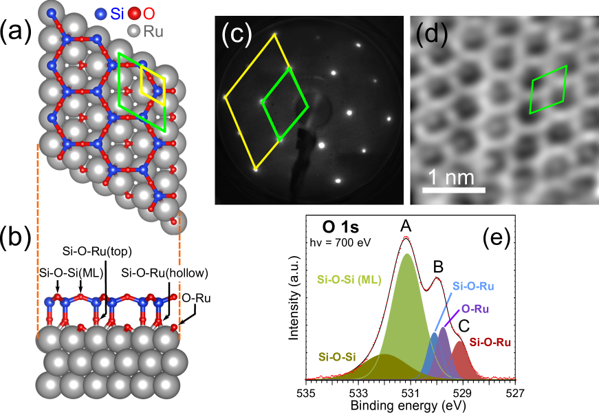
In a first experimental setup, a ML-film was elaborated following the preparation method described in the Materials and Methods section. It shows a sharp () LEED pattern (Figure 1c) and a honeycomb structure in STM (Figure 1d) with the presence of interfacial O atoms visible as protrusions at the center of the hexagons typical of an "O-rich" phase, confirming recent results from litterature25, 28. This phase has been predicted as the stable phase for the ML by earlier DFT calculations 21.
According to the ML structural model depicted in Figure 1a, O atoms occupy three sites on Ru: interfacial atoms are adsorbed on Ru hollow sites (O–Ru). When bonded to Si and forming Si–O–Ru linkages, O is adsorbed on Ru hollow– (Si-O–Ru(hollow)) or top (Si–O–Ru(top)) sites. O atoms bonded to two Si atoms are found in the topmost layer of the ML (Si–O–Si(ML)).
To try to detect the presence of these chemically different kinds of O atoms, we measured XPS with unprecedented high-resolution at a photon energy of = 700 eV. The measured spectra exhibit three peaks (see Figure 1e). Peak A at 531.1 eV binding energy (BE) is attributed to O bonded to two Si atoms (Si–O–Si(ML), light green) in the ML as already observed on the same system on Ru(0001)18 as well as on Mo(112) 12. The A peak has an extended high BE-tail, which suggests that it actually comprises two components. The higher-BE component (Si–O–Si, dark green), which obviously has less spectral weight than the one around 531.1 eV, may relate most probably to bonds between Si and O atoms for instance in a small fraction of the surface being covered with a BL 17 or to locally different chemical environments corresponding to structural defects or inhomogeneities in the "free" oxygen phase on Ru(0001) coexisting with the silicon oxide.
In an initial fit attempt, based on XPS spectra recorded on O–p(22), O–(21), and 3O–(22) superstructures on Ru(0001) (see Figure S2a), we could reasonably assign peak B located at 529.9 eV BE to O atoms chemisorbed on Ru (refered as O–Ru). Peak C is assumed to be due to Si–O–Ru bonds. Note that, up to now, peak C has not been resolved for this system18. Starting from this fitting assumption, a ratio between O–Ru and Si–O–Ru contributions of 2:1 was obtained (see Figure S3a,b for details concerning the fitting procedure) which is not consistent with the one for a Si4O10–2O formula such as expected here (with an unique Si–O–Ru site) i.e. 1:2. Actually, to better fit the experimental data, peak B and C need to be decomposed with three contributions (see Figure S3c,d). In this case, peak B is deconvoluted into the O–Ru contribution at 529.8 eV (purple) and a second Si–O–Ru contribution at 530.1 eV (light blue) which originates from O bonded to Si and Ru. Finally, peak C is assigned to a second Si–O–Ru contribution (red). This analysis takes into account the two inequivalent sites for O in the Si–O–Ru bonds according to the structural model given in Figure 1a. Nevertheless, we can not assign unambiguously a priori the two Si–O–Ru linkages, i.e. whether O sits on a top or a hollow site of the substrate. We can note that analysis from simulated XPS–spectrum reported in the Figure 10b of B. Yang et al. 18 predicts that Si–O–Ru(hollow) and Si–O–Ru(top) are respectively at high and low binding energies positions. In that case the corresponding ratio extracted from XPS-spectrum for Si–O–Ru/O–Ru/Si–O–Ru contributions is equal to 1:1.1:1 which is in good agreement with the expected one (1:1:1) for the structural model presented in Figure 1a,b.
The expected ratio between the different components corresponding to chemically inequivalent O bonds in the system (Si–O–Si(ML), Si–O–Ru, O–Ru, Si–O–Ru) is 3:1:1:1. Our best fit to the experimental data yields a roughly twice stronger contribution for the Si–O–Si bonds (Figure S3d). The deviation from the expected ratio is due to stronger surface character of Si–O–Si bonds compared to the other ones as already observed for ML on Mo(112)12 and BL on Ru(0001)17 by varying the angle of emission with respect to the normal of the sample. One way to modify the weight of contributions with surface character is to adjust the photon energy. Here, we have increased this energy to 820 eV. In Figure 2a-c, we observe as expected that the Si–O–Si contribution is now significantly lower (by about 25%), while the O–Ru contribution constituting the B peak increases (about 45% with respect to Si–O–Ru components).
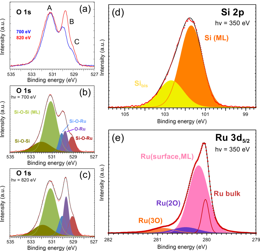
On the one hand, the decreased weight observed for Si–O–Si bonds can be explained by an increase of the inelastic mean free path (IMFP) of the electrons at high photon energy. On the other hand, the increased weight for O–Ru contribution has already been observed using higher photon energy, with regular X-ray lab source 18. The IMFP being marginally different for the three components (O–Ru, Si–O–Ru(top), Si–O–Ru(hollow)), it cannot explain such variations. A reasonable explanation could be a photodiffraction effect that may only be accounted for within a complex quantitative analysis of the XPS spectrum.
We also performed XPS measurements on the Si2p and Ru3d5/2 core levels (Figure 2d,e). The Si2p core level spectrum does not exhibit a single component. The spin-orbit coupling splitting of the core level, of about 600 meV, is too small to account for the lineshape. We hence assume that besides the main contribution centered at 101.7 eV (Si (ML)), at least one more contribution exists at 102.7 eV (Sibis), corresponding to a chemically inequivalent kind of Si atoms. Similar to the case of O atoms addressed earlier, such Si atoms may be found in a small fraction of the surface being covered with a BL silicon oxide or at defect sites.
We finally examine the Ru3d5/2 core level spectra after the growth of the silicon oxide ML (Figure 2e and Figure S2b), and compare it to the spectra obtained after forming an oxygen surface reconstruction consisting of 3O–(22) and (21) domains (identified by STM, not shown here). The oxidised surface spectrum is composed of four contributions which are due to inequivalent Ru atoms at the surface and in the bulk 44. Upon silicon oxide growth, bulk contribution remains and one extra surface component (Ru(surface,ML)) is observed at eV (pink) BE (see Figure 2e) that can be attributed to surface Ru atoms involved in Si–O–Ru bonds. In the case of the pure ML–phase, one would expect only two components: the bulk one and the surface one assigned to Si–O–Ru. However, Ru(2O) and Ru(3O) components are observed as well, possibly originating from inequivalent Ru atoms under residual BL regions, as already discussed in the cases of Si2p and O1s core levels.
Overall, our detailled high resolution XPS analysis provides fine insights into the binding of silicon oxide on Ru(0001). Our data detects chemically inequivalent contributions of bonds involving oxygen, silicon, and ruthenium atoms, which could not be directly deciphered, so far, due to a limited energy resolution of the measured XPS data. In particular, we are able to confirm the binding scheme that has been proposed up to now, in which the ML silicon oxide forms two distinct bonds with Ru(0001), via Si–O–Ru bridges involving two kinds of Ru atoms, three ones in hollow sites on one hand, and a single one on top sites on the other hand.
Dispersive electronic states in the monolayer of ultrathin silicon oxide. Now that we have established the chemical binding configuration at the interface between silicon oxide and Ru(0001), we turn to the exploration of the band structure of the system. Figure 3a-c displays ARPES spectra along the high symmetry line (see Figure S4 for details concerning the directions in the Brillouin zone (BZ)) of the bare substrate, the pre-oxidized 3O–(22)/Ru(0001) and after 2D silicon oxide formation, respectively. Full density of states (FDOS) (i.e. integrated over all the points accessible with the measurement) are given in Figure 3d. The band-structure calculated with DFT for the optimized geometry corresponding to bare Ru(0001), the 3O–(22)/Ru(0001) case, and the Si4O10–2O structural model presented in Figure 1a,b, are displayed in Figure 3d.
The ARPES spectrum of bare Ru(0001) (Figure 3a) is characterized by (i) a group of dispersive bands "A" in the range [0,-4] eV below Fermi level (EF), (ii) an upward dispersing band "B" at -6 eV around and (iii) a band labelled "C" at about -8 eV in good agreement with literature 45. These states are of sp– and d– like character. The flat band "D" lying at -10.5 eV originates from residual carbon contamination; its intensity varies with surface preparation conditions.
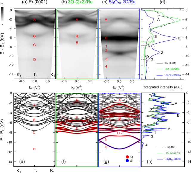
Upon O chemisorption, the ARPES spectrum is mostly modified below -6 eV where an extra band "E" is observed with a minimum at point at about -7 eV. Band "B" is marginally affected by the presence of O. In addition, we observe spectral weight near at -2 eV (band "A") and a decrease of the Ru-related intensity (compare to Figure 3a) that exhibits a (22) superperiodicity with respect to the substrate and resulting from Ru–O covalent bonds (see Figure S5). We note that the "D" band has vanished as could be expected since oxygen exposure to obtain the superstructures is a common way to get rid of carbon contamination on Ru surfaces. Experimental data are well reproduced by the DFT calculations of both the bare and oxygen-reconstructed surfaces (Figure 3e,f), specially the fact that ARPES spectrum is featureless below -8 eV. In order to simplify the interpretation, we have colorized in red the bands with an oxygen character. In comparaison with the case of the bare surface, the calculations for the 3O–(22) reconstruction exhibit new bands with oxygen character near -2 eV, -6 eV and -8 eV. These calculations match well with the ARPES measurements.
After the growth of the silicon oxide, four bands, labelled "1" to "4" in Figure 3c, are observed in the [-8,-14] eV range below EF. Band "1" is almost flat and located at about -8 eV. Bands "2" and "3" cross at -9.5 eV and disperse downwards and upwards around point, respectively. Band "4" disperses downwards with a minimum at at -13 eV. Note that band "4" is exclusively observed in the second BZ due to matrix elements effects as shown in Figure S6. In the [-5,-7] eV range, additional spectral weight is now observed. The FDOS in this range, displayed in Figure 3d, is broadened. In addition to the dispersive "B" band from 3O–(22)/Ru at -5 eV, a new flat band is found in this energy range. Moreover, a strong reduction of the photoemission intensity just below EF is visible (bands "A"), presumably due to the presence of the oxide limiting the escape of photoelectrons created underneath it, as it is expected given the surface sensitivity of the technique.
These features are globally reproduced by our DFT calculations displayed in Figure 3g. In particular, calculations show the emergence of non dispersive states around -5 eV (bands "B") and dispersive states in the [-7,-12] eV range that are not present in the case of the bare and oxidized surfaces. These new states have an oxygen and a silicon nature (or mixed oxygen–silicon) which put in evidence by red and blue colors respectively. The interpretation of the different bands will be discussed below on the basis of light-polarization-dependent ARPES data and projected density of states (PDOS) calculations. We can already mention that the shape of the different bands is well reproduced by DFT . The relative energies of the bands are also nicely reproduced, but not their absolute positions, which are rigidly shifted by about -2 eV. A closer inspection reveals a few differences between the experimental data and the DFT calculations. First the relative positions of the bands "1" and "2" are not well reproduced by the calculations. Second the crossing between the bands "2" and "3" at the point is not found in the calculations.
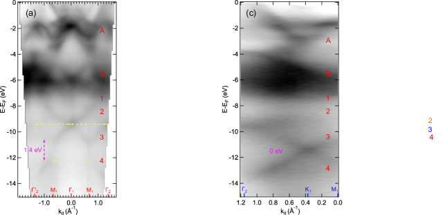
We also measured the band structure of silicon oxide along the and directions (Figure 4a,c). In these directions, the "A" bands show a twice smaller periodicity (here in reciprocal space) than that corresponding to the Ru(0001) lattice. These bands have the same properties in the case of Ru(0001) covered with the silicon oxide and with the 3O–(22) (Figure S5) and are thus ascribed to the formation of O–Ru bonds. This signature in the band structure corresponds to the reminiscence of O atoms only connected to the Ru substrate in the ML structure (see Figure 1a,b), as discussed above when analysing the HR-XPS data.
Furthermore, we can again identify bands numbered "1" to "4" and the group of bands labelled "B". These bands disperse in both high symmetry directions. We mapped an extended region of reciprocal space, giving us access to high symmetry points in the second BZ of the system. We now address the superperiodicity of the silicon oxide states relative to the Ru(0001) unit cell. For both the "2-3" and "4" bands, we measure a reciprocal space periodicity of (1.34 0.05) Å-1 (yellow dotted arrows in Figure 4a), which matches the Ru(0001) lattice vector in reciprocal space (=0.775 Å-1). Concerning the Ru states, their periodicity is two times bigger and equal to (2.71 0.05) Å-1. This point is fully coherent with the fact that silicon oxide has a () supercell in the direct space.
There is overall agreement between the DFT calculations and the ARPES data acquired in the direction (Figure 4b,d). The "3-4" bands are well reproduced. The calculated band structure of 2D silicon oxide reveals few bands with a (22) superperiodicity that are absent in the case of pristine and oxidized Ru surfaces (see also Figure S7). Above -7 eV below EF, a band–to–band comparison is less straightforward due to the large number of bands.
Interestingly, bands "3" and "4" touch at a single kind of high symmetry point in the BZ, the points (Figure 4c,d). At the vicinity of this point, the dispersion is linear (see Figure 4c,d and the second derivative shown in Figure S8d), characteristic of a Dirac point. Away from these points, a non-zero bandgap exists. In fact, as can be observed in scans of the band structure along the and directions (Figure 4), a saddle point is found for the "3" and "4" bands at the M points. To assess the bandgap between these two saddle points we extracted energy distribution curves (EDC) at and points (Figure S8b,c). From these curves we estimate the bandgap to (1.4 0.1) eV.
Origin of electronic bands. In the following, we address the orbital character of the electronic bands. For that purpose, we investigate the symmetry of the bands by adjusting the polarization of light (linear vertical (LV) and linear horizontal (LH)), and confront the experimental ARPES data to PDOS calculations considering the different kinds of atoms (Ru surface atoms, 4 O atoms and 2 Si atoms) composing silicon oxide as depicted in Figure 6b).
The ARPES spectra of ML silicon oxide, measured with both LV and LH polarizations, are shown in Figure 5a-d. Second derivative is used in order to increase the visiblity of bands with a low photoemission intensity. The corresponding FDOS for both polarizations is given in Figure 5e. The contributions at -2 eV ("A") and at -5 eV (shoulder of block "B" at low BE) below EF are assigned to hybridised states between Ru and O 17. Indeed these states were already present in the case of the 3O–(22)/Ru(0001) reconstruction (see Figure 3b and Figure S5). Furthermore, they mostly correspond to the density of states observed for the pz orbital of O1 atom and d orbitals of Ru atoms according to our calculations in Figure 6.
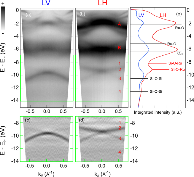
An increase of the spectral weight associated to the group of bands labeled "B" is observed in [-4,-6] eV range, compared to the case of 3O–(22)/Ru(0001). This increase has already been observed in amorphous SiO2 and GeO2 46, 47, in crystalline ML silicon oxide on Mo(112) 7, 9, 12, and in BL silicon oxide on Ru(0001) 17, and can be attributed to O2p non bonding states involving O atoms in Si–O–Si bonds of the topmost atomic layer. This is consistent with the PDOS of O4 atoms which contribute to those bonds in Figure 6d. Nevertheless, oxygen atoms O2 and O3 involved in Si–O–Ru(hollow) and Si–O–Ru(top) bonds also display non negligible PDOS in this energy range and might also participate in the total spectral weight, in particular with non bonding flat states with px and py symmetry.
The most probable origin of bands "1" and "2" is an hybridisation of pz orbitals from O and Si atoms in Si–O–Ru bonds connecting the silicon oxide sheet to the ruthenium substrate. On the one hand, these bands are drastically dependent on polarization: they are only observed with LH polarized light (see second derivative data in Figure 5c-d). This point can be understood by considering the expression of the photoemission intensity, in particular by considering parity arguments48, 49 given rise to particular selection rules for a given light polarization and a given probed initial state. In this way, it is possible to demonstrate that LV polarization is in–plane sensitive but not out–of–plane sensitive and yields no signal in the latter case. On the contrary, LH is both in–plane and out–of–plane sensitive. Using these arguments, bands "1" and "2", which are drastically affected by the modification of the polarization, can be experimentally attributed to out–of–plane covalent Si–O–Ru bonds. On the other hand, our calculations exhibit a large contribution of pz orbitals from Si1/O2 and Si2/O3 atoms in the [-7,-8] eV energy range. This is confirmed by the PDOS contribution of Ru surface atoms (d orbitals) in the corresponding energy range (see Figure 6a). Even if bands "1" and "2" are not well reproduced by our DFT calculations and hardly distinguishable in comparison to the ARPES data, we can still conclude on their Si–O–Ru origin. These bands are indeed absent for an O reconstruction on Ru(0001) (Figure 3b) and for a BL silicon oxide (data not shown).
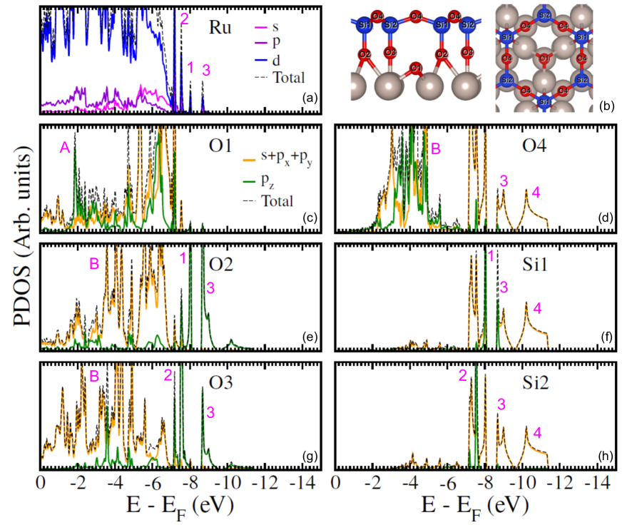
Concerning band "3", we observe photoemission intensity with both LH and LV polarizations (maximum in the case of LV). Following the same line of thoughts as before, we conclude that this band has an in–plane character. This is partially confirmed by our PDOS calculations, which indicate that this state emerges from hybridisation in the Si–O–Si bonds at -9 eV from O4 and Si1,2 atoms. Nevertheless, Ru surface, O2 and O3 atoms also exhibit non negligible spectral weight in this energy range which contradicts our interpretation in terms of polarization arguments.
We note that this state has already been observed in other silicon oxide compounds whose structure involves only Si–O–Si bonds: amorphous SiO2 46 and silicon oxide BL 17 though its dispersion was not resolved so far. This last point is coherent with an interpretation of band "3" as a Si–O–Si contribution, rather than a Si–O–Ru contribution that cannot exist in the silicon oxide BL.
The last band numbered "4", visible in the second BZ (Figure S8) and not in the first one (Figure 5b,d), can also be assigned to Si–O–Si bonds. Indeed this band appears in both LH and LV cases. In addition, calculations predict DOS from orbitals of O4 atoms and from orbitals of Si1,2 atoms in the energy range of [-10,-11.5] eV below EF. This interpretation is also corroborated by the absence of a PDOS contribution of Ru surface atoms as described in Figure 6a. This band is unambiguously due to an hybridisation of O4 and Si1,2 orbitals at the top of the silicon oxide layer.
Overall, the ML silicon oxide on Ru(0001) is characterized by at least four inequivalent dispersive bands. Two of them are presumably due to out–of–plane Si–O–Ru covalent bonds connecting the silicon oxide sheet to its substrate, and two others are due to in–plane Si–O–Si bonds in the topmost plane of silicon oxide sheet. While Si–O–Si bands are well reproduced by DFT calculations using the generally accepted relaxed model shown in Figure 1a,b, it is not the case of Si–O–Ru ones. Indeed, in addition to a global energy shift, contributions "1–2" are found at too low BE, and the degeneracy of bands "2" and "3" is lifted at the point, unlike in the ARPES measurements.
In the DFT calculation we have considered the atomic model initially proposed in Ref. 18 for the monolayer silicon oxide. The precise epitaxial relationship of this model (hollow-top) was further supported by combining DFT calculations and atomically-resolved STM images 25 and is confirmed by the present XPS measurements (cf Figure 2e). Indeed, we report two well defined contributions for the Ru–O–Si bonds which energies are separated by 1 eV. This highlights a complex bond character in the two Ru–O–Si bridges linking the monolayer silicon oxide to the ruthenium surface.
One striking feature in the calculated band structure is the presence of five bands (Figure 3g) while only four bands are observed in the ARPES. Moreover, band "3" is flattened in leading to an apparent gap opening due to an anti-crossing with the next bands. We can assume that for the same reason, some degeneracy are raised between two bands in the calculation leading to five bands instead of four. In other words, it is likely that band "1" or band "2" are degenerated in the experimental band structure.
In order to evaluate the chemistry of the Ru–O–Si bridges, we have tested different possible origins for the discrepancy between theoretical and experimental band structures: i/ epitaxial relationship ii/ number of ruthenium layers that could change the electrostatics at the Ru surface. However, all the high symmetry shifts relaxed to the present model. Likewise increasing the number of Ru layers does not allow to recover the experimental behavior at the point (See Figure S10b).
An other possible source of discrepancy might come from the used level of approximation in the DFT calculations. Indeed the present system is an hybrid one that contains different type of bondings ranging from covalent to metallic and might be highly sensitive to the used approximations. This hypothesis was tested by considering a bunch of different exchange and correlation (XC) functional including local (LDA) semi-local (PBE, SCAN) and hybrid (HSE06) descriptions. In Figure S10c we report the band structure for the SCAN functional that displays a small but rigid downward shift of the five characteristic bands. All the other considered XC functionals show the same behavior as depicted in Figure S11 by the evolution of the five characteristic eigenvalues at the point. We note that the HSE06 functional seems to better reproduce the position of the eigenvalues "4" and "3" in connection with the expected band gap underestimation for local XC functionals.
Conclusions
In conclusion, we were able to resolve the binding configuration of ML of silicon oxide on Ru(0001). Two kinds of Si–O–Ru bridges involving two chemically inequivalent Ru atoms are formed. They result in the existence of two sublattices in the honeycomb lattice of ML silicon oxide. We discovered four electronic bands below Fermi level. Two of them form a Dirac cone, and two others are semi-flat bands. The existence of the two sub-lattices translates in the formation of a large band gap. All together the band structure is reminiscent of that typical of Kagome lattices. In addition, we demonstrate that the acknowledged atomic model for ML silicon oxide is incomplete as it presents few inconsistencies with our experimental data. Further characterizations are required to probe a better model.
Our work opens the way to the exploration of topologically non trivial electronic band structures in ultimately thin oxides which may eventually be controlled efficiently via local electric fields owing to the two-dimensional character of the system, for instance with the help of adsorbed species or dielectric gates.
Materials and methods
Experiment. Experiments were carried out in three ultra–high vacuum (UHV) setups ( mbar). The first one is equipped with a low temperature STM (LT–STM) operating at T K, LEED, ARPES and XPS. The second one is equipped with a monochromated X-rays source (Al Kα, resolution better than 300 meV) and a high energy, momentum and spin photoemission analyser (DA30-L from VG–SCIENTA). Finally, the third one is the end station of the CASSIOPEE beamline at synchrotron SOLEIL, equipped with LEED, Auger electron spectroscopy (AES), high energy and momentum resolution ARPES (10 meV and 0.01 , respectively) and XPS (70 meV) using a VG–SCIENTA R analyzer. Photoemission measurements were recorded at K. ARPES was performed with light polarization either linear vertical or linear horizontal. Details about the experimental geometry are given in Figure S1 in supporting information (SI). A clean Ru(0001) surface was obtained by repeated cycles of Ar+ sputtering and annealing up to K followed by molecular oxygen exposure and flash annealing resulting in a sharp () LEED pattern (not shown here). The absence of contamination was checked by XPS and ARPES. After cleaning, Ru3d5/2 core levels exhibit a surface-related contribution at a binding energy of eV (not shown here). A ML silicon oxide was grown on an oxygen-covered Ru(0001) surface forming a so-called 3O–(22)50 reconstruction observed with LEED, XPS, APRES and LT-STM. The latter reconstruction was obtained by exposing Ru(0001) at mbar O2 at K for min. Then silicon was evaporated using electron bombardment of a high purity Si rod (> 99.9999 ) under an oxygen pressure of mbar at room temperature (RT). The Si deposition rate was calibrated using AES for a well-documented system, Si on Cu(100) 51. The final crystallization step was performed under mbar O2 at K for min followed by a slow temperature ramp at a rate of C min-1 down to RT. Temperatures were measured using a pyrometer.
Computational details. The theoretical study was carried out by using first principles calculations based on density functional theory (DFT). The exchange correlation potential was treated within the Local Spin-Density L(S)DA approximation Ceperley1980-LDA. The Projected Augmented Wave (PAW) method 52 was used to solve the Kohn-Sham equations as implemented in the Vienna ab-initio Simulation Package (VASP) 53 with a kinetic energy cut-off for the plane-wave expansion of 490 eV. The Ruthenium (0001) surface cleaved from a hcp lattice where the crystal lattice parameter was firstly optimized. We have considered three atomic layers that is expected to be enough to reproduce bulk properties of the growth support 18. The equilibrium geometry of Oxygen adsorbed and silicon oxide supported on the Ru(0001) surface was obtained by relaxing the Oxygen/silicon oxide and external Ruthenium ion positions while the deepest Ruthenium layer was kept fixed. The optimization of atomic positions was performed using conjugate gradient algorithm until the Hellmann-Feynman forces reach the threshold of 0.1 eV/Å. A vacuum of at least 12 Å was employed along the z-direction to avoid undesired interactions between periodic layers. The Brillouin zone was sampled with a k-point mesh in the self-consistent energy calculations and increased to a denser mesh in the density of states calculation.
Supporting Information includes details concerning the experimental geometry used for photoemission measurements, discussion of line shapes used in XPS data fitting procedure, surface Brillouin zone details, ARPES data for the 3O–(22)/Ru(0001) superstructure, additional ARPES data in the second Brillouin zone for ultrathin silicon oxide and complementary band structure DFT calculations.
1 Author Information
*E-mail: geoffroy.kremer@univ-lorraine.fr
2 Associated Content
The authors declare no competing financial interest.
This work was supported by the 2DTransformers project under the OH-RISQUE program of the French National Research Agency (ANR-14-OHRI-0004). We would like to thank the team Dam for the helpful assistance during the connection and the installation of the new SR–ARPES setup on the Tube. The DFT calculations were done using French supercomputers (GENCI, # 6194) and the Predictive Simulation Center facility that gathers in Grenoble SPINTEC, LSim and Leti. We thanks Professor N. Mousseau for useful discussions. C. G. acknowledges financial support from the Spanish Ministry of Science, Innovation and Universities through the project MAT2017-88258-R and the "Mariá de Maeztu" program for units of excellence in R & D (grant no. MDM-2014-0377).
References
- Pacchioni et al. 1992 Pacchioni, G., Bagus, P. S., Parmigiani, F., Eds. Cluster Models for Surface and Bulk Phenomena; Springer US, 1992
- Granqvist 2007 Granqvist, C. G. Transparent conductors as solar energy materials: A panoramic review. Sol. Energ. Mat. Sol. C. 2007, 91, 1529 – 1598
- Freund 2012 Freund, H.-J. In Oxide Ultrathin Films; Pacchioni, G., Valeri, S., Eds.; Wiley-VCH: Weinheim, 2012; Chapter 7, pp 145–179
- Kumar et al. 2012 Kumar, B.; Llorente, M.; Froehlich, J.; Dang, T.; Sathrum, A.; Kubiak, C. P. Photochemical and Photoelectrochemical Reduction of CO2. Annu. Rev. Phys. Chem. 2012, 63, 541–569
- Schintke et al. 2001 Schintke, S.; Messerli, S.; Pivetta, M.; Patthey, F.; Libioulle, L.; Stengel, M.; De Vita, A.; Schneider, W.-D. Insulator at the Ultrathin Limit: MgO on Ag(001). Phys. Rev. Lett. 2001, 87, 276801
- Kundu and Murata 2002 Kundu, M.; Murata, Y. Growth of single-crystal SiO2 film on Ni(111) surface. Appl. Phys. Lett. 2002, 80, 1921–1923
- Schroeder et al. 2002 Schroeder, T.; Giorgi, J. B.; Bäumer, M.; Freund, H.-J. Morphological and electronic properties of ultrathin crystalline silica epilayers on a Mo(112) substrate. Phys. Rev. B 2002, 66, 165422
- Weissenrieder et al. 2005 Weissenrieder, J.; Kaya, S.; Lu, J.-L.; Gao, H.-J.; Shaikhutdinov, S.; Freund, H.-J.; Sierka, M.; Todorova, T. K.; Sauer, J. Atomic Structure of a Thin Silica Film on a Mo(112) Substrate: A Two-Dimensional Network of SiO4 Tetrahedra. Phys. Rev. Lett. 2005, 95, 076103
- Wendt et al. 2005 Wendt, S.; Ozensoy, E.; Wei, T.; Frerichs, M.; Cai, Y.; Chen, M. S.; Goodman, D. W. Electronic and vibrational properties of ultrathin SiO2 films grown on Mo(112). Phys. Rev. B 2005, 72, 115409
- Sierka et al. 2006 Sierka, M.; Todorova, T. K.; Kaya, S.; Stacchiola, D.; Weissenrieder, J.; Lu, J.; Gao, H.; Shaikhutdinov, S.; Freund, H.-J.; Sauer, J. Interplay between theory and experiment in the quest for silica with reduced dimensionality grown on a Mo(112) surface. Chem. Phys. Lett. 2006, 424, 115–119
- Todorova et al. 2006 Todorova, T. K.; Sierka, M.; Sauer, J.; Kaya, S.; Weissenrieder, J.; Lu, J.-L.; Gao, H.-J.; Shaikhutdinov, S.; Freund, H.-J. Atomic structure of a thin silica film on a Mo(112) substrate: A combined experimental and theoretical study. Phys. Rev. B 2006, 73, 165414
- Kaya et al. 2007 Kaya, S.; Baron, M.; Stacchiola, D.; Weissenrieder, J.; Shaikhutdinov, S.; Todorova, T.; Sierka, M.; Sauer, J.; Freund, H.-J. On the geometrical and electronic structure of an ultra-thin crystalline silica film grown on Mo(112). Surf. Sci. 2007, 601, 4849–4861
- Zhang et al. 2008 Zhang, Z.; Jiang, Z.; Yao, Y.; Tan, D.; Fu, Q.; Bao, X. Preparation and characterization of atomically flat and ordered silica films on a Pd(100) surface. Thin Solid Films 2008, 516, 3741–3746
- Löffler et al. 2010 Löffler, D.; Uhlrich, J. J.; Baron, M.; Yang, B.; Yu, X.; Lichtenstein, L.; Heinke, L.; Büchner, C.; Heyde, M.; Shaikhutdinov, S.; Freund, H.-J.; Włodarczyk, R.; Sierka, M.; Sauer, J. Growth and Structure of Crystalline Silica Sheet on Ru(0001). Phys. Rev. Lett. 2010, 105, 146104
- Lichtenstein et al. 2012 Lichtenstein, L.; Büchner, C.; Yang, B.; Shaikhutdinov, S.; Heyde, M.; Sierka, M.; Włodarczyk, R.; Sauer, J.; Freund, H.-J. The Atomic Structure of a Metal-Supported Vitreous Thin Silica Film. Angew. Chem. Int. Ed. 2012, 51, 404–407
- Lichtenstein et al. 2012 Lichtenstein, L.; Heyde, M.; Ulrich, S.; Nilius, N.; Freund, H.-J. Probing the properties of metal oxide interfaces: silica films on Mo and Ru supports. J. Phys.: Condens. Matter 2012, 24, 354010
- Włodarczyk et al. 2012 Włodarczyk, R.; Sierka, M.; Sauer, J.; Löffler, D.; Uhlrich, J. J.; Yu, X.; Yang, B.; Groot, I. M. N.; Shaikhutdinov, S.; Freund, H.-J. Tuning the electronic structure of ultrathin crystalline silica films on Ru(0001). Phys. Rev. B 2012, 85, 085403
- Yang et al. 2012 Yang, B.; Kaden, W. E.; Yu, X.; Boscoboinik, J. A.; Martynova, Y.; Lichtenstein, L.; Heyde, M.; Sterrer, M.; Włodarczyk, R.; Sierka, M.; Sauer, J.; Shaikhutdinov, S.; Freund, H.-J. Thin silica films on Ru(0001): monolayer, bilayer and three-dimensional networks of [SiO4] tetrahedra. Phys. Chem. Chem. Phys. 2012, 14, 11344
- Yu et al. 2012 Yu, X.; Yang, B.; Anibal Boscoboinik, J.; Shaikhutdinov, S.; Freund, H.-J. Support effects on the atomic structure of ultrathin silica films on metals. Appl. Phys. Lett. 2012, 100, 151608
- Altman et al. 2013 Altman, E. I.; Götzen, J.; Samudrala, N.; Schwarz, U. D. Growth and Characterization of Crystalline Silica Films on Pd(100). J. Phys. Chem. C 2013, 117, 26144–26155
- Shaikhutdinov and Freund 2013 Shaikhutdinov, S.; Freund, H.-J. Ultrathin Silica Films on Metals: The Long and Winding Road to Understanding the Atomic Structure. Adv. Mater. 2013, 25, 49–67
- Yang et al. 2013 Yang, B.; Boscoboinik, J. A.; Yu, X.; Shaikhutdinov, S.; Freund, H.-J. Patterned Defect Structures Predicted for Graphene Are Observed on Single-Layer Silica Films. Nano Lett. 2013, 13, 4422–4427
- Crampton et al. 2015 Crampton, A. S.; Ridge, C. J.; Rötzer, M. D.; Zwaschka, G.; Braun, T.; DÉlia, V.; Basset, J.-M.; Schweinberger, F. F.; Günther, S.; Heiz, U. Atomic Structure Control of Silica Thin Films on Pt(111). J. Phys. Chem. C 2015, 119, 13665–13669
- Fischer et al. 2015 Fischer, F. D.; Sauer, J.; Yu, X.; Boscoboinik, J. A.; Shaikhutdinov, S.; Freund, H.-J. Ultrathin Ti-Silicate Film on a Ru(0001) Surface. J. Phys. Chem. C 2015, 119, 15443–15448
- Mathur et al. 2015 Mathur, S.; Vlaic, S.; Machado-Charry, E.; Vu, A.-D.; Guisset, V.; David, P.; Hadji, E.; Pochet, P.; Coraux, J. Degenerate epitaxy-driven defects in monolayer silicon oxide on ruthenium. Phys. Rev. B 2015, 92, 161410(R)
- Yang et al. 2015 Yang, B.; Shaikhutdinov, S.; Freund, H.-J. Ultrathin silicatene/silicon-carbide hybrid film on a metal substrate. Surf. Sci. 2015, 632, 9–13
- Klemm et al. 2016 Klemm, H.; Peschel, G.; Madej, E.; Fuhrich, A.; Timm, M.; Menzel, D.; Schmidt, T.; Freund, H.-J. Preparation of silica films on Ru(0001): A LEEM/PEEM study. Surf. Sci. 2016, 643, 45–51
- Mathur 2016 Mathur, S. Growth and atomic structure of a novel crystalline two-dimensional material based on silicon and oxygen. Ph.D. thesis, Université Grenoble Alpes, 2016
- Büchner and Heyde 2017 Büchner, C.; Heyde, M. Two-dimensional silica opens new perspectives. Prog. Surf. Sci. 2017, 341–374
- Jhang et al. 2017 Jhang, J.-H.; Zhou, C.; Dagdeviren, O. E.; Hutchings, G. S.; Schwarz, U. D.; Altman, E. I. Growth of two dimensional silica and aluminosilicate bilayers on Pd(111): from incommensurate to commensurate crystalline. Phys. Chem. Chem. Phys. 2017, 19, 14001–14011
- Li et al. 2017 Li, L.; Tissot, H.; Shaikhutdinov, S.; Freund, H.-J. Transition Metal Induced Crystallization of Ultrathin Silica Films. Chem. Mater. 2017, 29, 931–934
- Büchner et al. 2016 Büchner, C.; Wang, Z.-J.; Burson, K. M.; Willinger, M.-G.; Heyde, M.; Schlögl, R.; Freund, H.-J. A Large-Area Transferable Wide Band Gap 2D Silicon Dioxide Layer. ACS Nano 2016, 10, 7982–7989
- Włodarczyk et al. 2013 Włodarczyk, R.; Sauer, J.; Yu, X.; Boscoboinik, J. A.; Yang, B.; Shaikhutdinov, S.; Freund, H.-J. Atomic Structure of an Ultrathin Fe-Silicate Film Grown on a Metal: A Monolayer of Clay? J. Am. Chem. Soc. 2013, 135, 19222–19228
- Yang et al. 2015 Yang, B.; Shaikhutdinov, S.; Freund, H.-J. Ultrathin silicatene/silicon-carbide hybrid film on a metal substrate. Surf. Sci. 2015, 632, 9–13
- Jerratsch et al. 2009 Jerratsch, J. F.; Nilius, N.; Freund, H.-J.; Martinez, U.; Giordano, L.; Pacchioni, G. Lithium incorporation into a silica thin film: Scanning tunneling microscopy and density functional theory. Phys. Rev. B 2009, 80, 245423
- Martinez et al. 2009 Martinez, U.; Jerratsch, J.-F.; Nilius, N.; Giordano, L.; Pacchioni, G.; Freund, H.-J. Tailoring the Interaction Strength between Gold Particles and Silica Thin Films via Work Function Control. Phys. Rev. Lett. 2009, 103, 056801
- Ulrich et al. 2009 Ulrich, S.; Nilius, N.; Freund, H.-J.; Martinez, U.; Giordano, L.; Pacchioni, G. Realization of an atomic sieve: Silica on Mo(112). Surf. Sci. 2009, 603, 1145–1149
- Zhong et al. 2017 Zhong, J.-Q.; Wang, M.; Akter, N.; Kestell, J. D.; Boscoboinik, A. M.; Kim, T.; Stacchiola, D. J.; Lu, D.; Boscoboinik, J. A. Immobilization of single argon atoms in nano-cages of two-dimensional zeolite model systems. Nat. Commun. 2017, 8, 16118
- Ben Romdhane et al. 2013 Ben Romdhane, F.; Björkman, T.; Rodríguez-Manzo, J. A.; Cretu, O.; Krasheninnikov, A. V.; Banhart, F. In Situ Growth of Cellular Two-Dimensional Silicon Oxide on Metal Substrates. ACS Nano 2013, 7, 5175–5180
- Björkman et al. 2013 Björkman, T.; Kurasch, S.; Lehtinen, O.; Kotakoski, J.; Yazyev, O. V.; Srivastava, A.; Skakalova, V.; Smet, J. H.; Kaiser, U.; Krasheninnikov, A. V. Defects in bilayer silica and graphene: common trends in diverse hexagonal two-dimensional systems. Sci. Rep. 2013, 3, 03482
- Roy and Heuer 2019 Roy, P. K.; Heuer, A. Ring Statistics in 2D Silica: Effective Temperatures in Equilibrium. Phys. Rev. Lett. 2019, 122, 016104
- Lewandowski et al. 2018 Lewandowski, A. L.; Schlexer, P.; Büchner, C.; Davis, E. M.; Burrall, H.; Burson, K. M.; Schneider, W.-D.; Heyde, M.; Pacchioni, G.; Freund, H.-J. Atomic structure of a metal-supported two-dimensional germania film. Phys. Rev. B 2018, 97, 115406
- Lewandowski et al. 2018 Lewandowski, A. L.; Schlexer, P.; Tosoni, S.; Gura, L.; Marschalik, P.; Büchner, C.; Burrall, H.; Burson, K. M.; Schneider, W.-D.; Pacchioni, G.; Heyde, M. Determination of Silica and Germania Film Network Structures on Ru(0001) at the Atomic Scale. J. Phys. Chem. C 2018,
- Lizzit et al. 2001 Lizzit, S.; Baraldi, A.; Groso, A.; Reuter, K.; Ganduglia-Pirovano, M. V.; Stampfl, C.; Scheffler, M.; Stichler, M.; Keller, C.; Wurth, W.; Menzel, D. Surface core-level shifts of clean and oxygen-covered Ru(0001). Phys. Rev. B 2001, 63, 205419
- Nguyen et al. 2013 Nguyen, N.; Mulazzi, M.; Reinert, F. Electronic structure and Fermi surface of Ru(0001) and Ru(100) measured with high-resolution angle-resolved photoemission. J. Electron Spectrosc. Relat. Phenom. 2013, 191, 27–34
- DiStefano and Eastman 1971 DiStefano, T. H.; Eastman, D. E. Photoemission Measurements of the Valence Levels of Amorphous SiO2. Phys. Rev. B 1971, 27, 1560–1562
- Fischer et al. 1977 Fischer, B.; Pollak, R. A.; DiStefano, T. H.; Grobman, W. D. Electronic structure of SiO2, SixGe1-xO2, and GeO2 from photoemission spectroscopy. Phys. Rev. B 1977, 15, 3193–3199
- Tejeda and Malterre 2015 Tejeda, A.; Malterre, D. Photoémission dans les solides: concepts et applications; EDP Sciences: Les Ulis, 2015
- Yukawa et al. 2013 Yukawa, R.; Yamamoto, S.; Ozawa, K.; D´Angelo, M.; Ogawa, M.; Silly, M. G.; Sirotti, F.; Matsuda, I. Electronic structure of the hydrogen-adsorbed SrTiO3(001) surface studied by polarization-dependent photoemission spectroscopy. Phys. Rev. B 2013, 87, 115314
- Kim et al. 1998 Kim, Y.; Wendt, S.; Schwegmann, S.; Over, H.; Ertl, G. Structural analyses of the pure and cesiated Ru(0001)-(22)-3O phase. Surf. Sci. 1998, 418, 267–272
- Lalmi et al. 2010 Lalmi, B.; Oughaddou, H.; Enriquez, H.; Kara, A.; Vizzini, S.; Ealet, B.; Aufray, B. Epitaxial growth of a silicene sheet. Appl. Phys. Lett. 2010, 97, 223109
- Blöchl 1994 Blöchl, P. E. Projector augmented-wave method. Phys. Rev. B 1994, 50, 17953–17979
- Kresse and Furthmüller 1996 Kresse, G.; Furthmüller, J. Efficient iterative schemes for ab initio total-energy calculations using a plane-wave basis set. Phys. Rev. B 1996, 54, 11169–11186
See pages 1-13 of SI.pdf