National Institute for Standards and Technology] Center for Nanoscale Science and Technology, National Institute for Standards and Technology, Gaithersburg, MD 20899, USA \alsoaffiliation[University of Maryland] Maryland NanoCenter, University of Maryland, College Park, MD 20742, USA National Institute for Standards and Technology] Center for Nanoscale Science and Technology, National Institute for Standards and Technology, Gaithersburg, MD 20899, USA Keywords— photovoltaics, grain boundary, thin film, polycrystalline semiconductor, carrier defect recombination
Quantitative theory of the grain boundary impact on the open-circuit voltage of polycrystalline solar cells
Abstract
Thin film polycrystalline photovoltaics are a mature, commercially-relevant technology. However, basic questions persist about the role of grain boundaries in the performance of these materials, and the extent to which these defects may limit further progress. In this work, we first extend previous analysis of columnar grain boundaries to develop a model of the recombination current of “tilted” grain boundaries. We then consider systems with multiple, intersecting grain boundaries and numerically determine the parameter space for which our analytical model accurately describes the recombination current. We find that for material parameters relevant for thin film photovoltaics, our model can be applied to compute the open-circuit voltage of materials with networks of inhomogeneous grain boundaries. This model bridges the gap between the distribution of grain boundary properties observed with nanoscale characterization and their influence on the macroscale device open-circuit voltage.
Polycrystalline materials possess an abundance of extended crystallographic defects in the form of grain boundaries, which are typically harmful to device performance. However, recent development in thin-film photovoltaics have led to surprisingly high efficiencies given the large densities of grain boundaries. 1 The efficiency records were obtained mostly by improvements in light absorption and collection of photogenerated carriers. 2 Increasing the open-circuit voltage (currently at in polycrystalline CdTe 2, 3) has proven to be more difficult. Two groups recently reported 4, 5 single crystal CdTe solar cells with open-circuit voltages above , suggesting that grain boundaries may be an important source of recombination and reduce the open-circuit voltage of polycrystalline solar cells 6. While grain boundaries are a predominant source of defects in thin film photovoltaics, a precise understanding of grain boundary recombination and its impact on performance remains uncertain and controversial. 7 A primary difficulty in experimentally determining the effect of grain boundaries is that modifying grain structure typically changes other important material properties 7 (as in the studies of Ref. 4, 5). Theoretical models are suited to provide guidance in this case, as models afford the freedom to independently vary material and system parameters. The simplest models of grain boundaries 8, 9, 10, 11 used for analyzing polycrystalline Si are inconsistent with the high efficiency of thin film photovoltaics, indicating the need for more sophisticated approaches.
On the experimental side, there has been recent substantial progress in characterizing grain boundaries. Nanoscale imaging and spectroscopy can, in some circumstances, reveal the full three-dimensional, chemically resolved atomic structure of grain boundaries. 12, 13 Knowledge of atomic structure enables first principles calculations of the electronic structure of certain ideal grain boundaries, identifying defect energy levels and charge states. 14 Direct measurements of electrical properties of individual grain boundaries using high resolution techniques yield qualitative insights (such as the sign of grain boundary defect charge 15, 16), although quantitative interpretation of these measurements remains a challenge. Nevertheless, even perfect knowledge of grain boundary electrical properties would not suffice to determine their impact on important figures of merit, such as the open-circuit voltage. This is due to a gap on the theory side: so far no analytical relation connects grain boundary properties of a realistic sample to its . Here we provide this previously missing component of the theory and demonstrate its validity for material parameters typical of thin film solar cells. While the short circuit current and the fill factor are also key elements of a solar cell efficiency, we focus on the open-circuit voltage as it is the metric for which the largest margin of improvement is available. 2
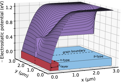
In a series of recent works, 1, 2 we studied the charge transport associated with isolated, columnar grain boundaries in thin film solar cells consisting of junctions (-type absorber). We obtained an approximate analytic solution for the grain boundary recombination current under the conditions that the grain boundary is positively charged with large defect density (so that the Fermi level is pinned to the defect neutrality level), and that the majority carrier transport is sufficiently facile so that the quasi-hole Fermi level varies by less than the thermal voltage ( at room temperature). Under these circumstances, electrostatic screening leads to downward band bending in the vicinity of the grain boundary (shown in Figure 1), which confines electrons near the grain boundary core. We showed that in this case, the two-dimensional problem for the recombination can be mapped to an effective one-dimensional problem for the motion of electrons along the grain boundary. The dark recombination current of an isolated columnar grain boundary versus voltage is shown to take the following general form 2
| (1) |
where is an effective surface recombination velocity, is the characteristic length over which recombination occurs, is the grain size, is an effective density of states, is an activation energy, is the ideality factor ( is the Boltzmann constant and is the temperature).
The specific form of the parameters depends on the type (i.e., majority carrier) of the grain boundary core. There are 3 possible cases: 1. -type, which occurs when the band bending at the grain boundary is large enough to cause type inversion at the grain boundary core (i.e. the Fermi level is closer to the conduction band at the grain boundary core), 2. -type, where we note that the assumption of downward band bending implies that the grain boundary core will always be less -type than the bulk of the absorber. For both -type and -type grain boundary cases, the majority carriers have a constant concentration along the entire length of the grain boundary. The last case is: 3. Neither -type or -type, a case to which we refer as “high recombination”. For this case, there are regions along the grain boundary core at which the electron and hole densities are similar in magnitude, and both carrier densities vary along the length of the grain boundary. The specific expressions of the parameters entering Eq. (1) are given in the Supporting Information and in Ref. 1.
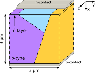
In this work, we focus on microstructures with complex grain boundary topology, as depicted in Figure 2. We first extend our previous model to consider grain boundaries tilted at an angle with respect to the junction normal. Based on the physical picture of carrier recombination developed in previous works, we make a simple ansatz for the dependence of grain boundary recombination on . To demonstrate the validity of this ansatz, we make comparisons to 2-d numerical simulations performed with the semiconductor modeling software Sesame 3. We next analyze the carrier transport in networks of non-columnar grain boundaries. We find that under similar assumptions leading to Eq. (1), the recombination of a particular grain boundary embedded within a network is approximately equal to the recombination of the same grain boundary in isolation. The total dark recombination current of a grain boundary network is therefore given by the sum of its individual contributions, which can be weighted by a statistical distribution of grain boundary parameter values. The description of the orientation-dependence and the network behavior of grain boundary recombination completes our model. These advances expand the applicability of the model from idealized, artificial geometries to real materials. Our model therefore provides a missing link between nanoscale characterization of the distribution of grain boundary properties and their impact on a real device open-circuit voltage .
We begin with a description of the charge transport of a single grain boundary with one end near the metallurgical junction, and oriented an angle , as shown in Figure 3b. We consider grain boundaries which do not make direct connections with the contacts. The physical picture we describe here is based on Ref. 1, which provides more details. Informed by numerical simulations, we first posit that the grain boundary orientation primarily affects the length over which recombination occurs along the grain boundary core. That is, of Eq. (1) is assumed to be the only -dependent factor. We start with some definitions. is defined as the junction depletion width in the grain interior, i.e. in a region where the electrostatic potential is unperturbed by the grain boundary (see Figure 3d). is defined as the position in the grain interior where (in equilibrium), such that for (see Figure 3c). The primary quantity of interest is the grain boundary recombination, which occurs at defects located at the grain boundary core. For -type or -type grain boundaries, the grain boundary defect recombination is set by the minority carrier concentration, while for high-recombination grain boundaries, both electron and hole density control the recombination. We summarize the behavior of the system for the three cases below.
For an -type grain boundary, recombination is determined by holes. Ref. 1 shows that holes flow from the bulk of the -type grain interior into the grain boundary core and recombine. The majority of the grain boundary length is embedded in -type bulk, so holes are available for transport into the grain boundary from the grain bulk over approximately the entire grain boundary length, independent of the orientation . The high defect density fixes the quasi-Fermi levels and the electrostatic potential over the entire length of the grain boundary, as shown in Figure 1. Electron and hole densities are therefore uniform along the grain boundary, leading to uniform recombination along the entire grain boundary length . Hence we have .
The recombination in a -type grain boundary is determined by electrons, which flow from the -type grain interior into the grain boundary core. For a perfectly columnar () grain boundary, the electrons flow into the grain boundary for , as shown in Figure 3a. The recombination is therefore concentrated within the -region of the junction depletion region, and is uniform for . As the grain boundary is tilted (), a larger section of the grain boundary is exposed to electrons coming from the nearby -contact, as shown in Figure 3b. This increased exposure expands the region of uniform recombination, which leads to a longer recombination region . We find the appropriate form for the increase in recombination length due to grain boundary tilting is , where represents the horizontal cross section of the segment of the grain boundary exposed to the electron flow in the depletion region.
Additional recombination occurs as electrons diffuse along the grain boundary, increasing . Note that electron transport is not confined to the grain boundary dislocation core (which is of atomic scale), but is spread out over the depletion width surrounding the grain boundary core. We denote the length scale for electron confinement near a grain boundary by ; for default material parameters (given in Table S2 of the Supporting Information) and moderate grain boundary potentials (e.g 250 eV), is on the order of . The effective lifetime of confined electrons is then given by , where is the effective grain boundary recombination velocity, and their diffusion length is , where is the diffusivity of the confined electrons (which may be reduced from the bulk value due to disorder at the grain boundary core). For large surface recombination velocities, diffusion lengths of confined electrons are small, and additional recombination away from the junction depletion width is negligible. For low surface recombination velocities, diffusion lengths of confined electrons are large and recombination is uniform along the entire grain boundary. The length of the recombination region in these two limits therefore reads
| (2) | |||||
| (3) |
Equation (2) is valid as long as is such that ; otherwise. Eq. (10) of the Supporting Information gives the general expression for -type grain boundary recombination for a general value of .
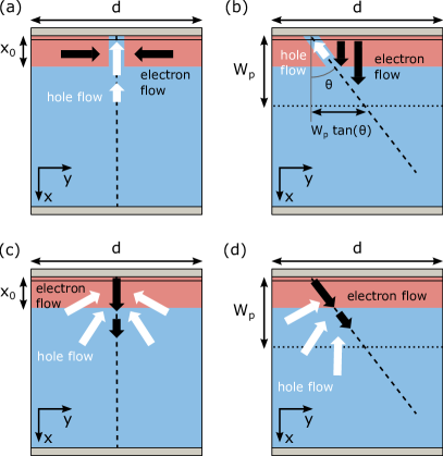
The high-recombination regime of the perfectly columnar grain boundary occurs at sufficiently high applied voltage so that both electron and hole densities are of comparable magnitude. In this case, grain boundary recombination is the result of both electron and hole currents flowing into the grain boundary core. Both carrier types are available only in the vicinity of the depletion region, so that currents flow as depicted in Figure 3c. Holes flow towards the junction depletion region to recombine with electrons flowing along the grain boundary core. The recombination is therefore peaked at a “hotspot” in the depletion region. 1 As the grain boundary is tilted, a longer section is exposed to hole flow in the depletion region, as shown in Figure 3d. This larger exposure increases the recombination region length in a manner similar to the previous -type grain boundary case: . Beyond this “hotspot” region, electrons diffuse in a one-dimensional motion along the grain boundary core, as in the -type grain boundary case described above. We find that the recombination region in the high-recombination regime reads
| (4) | |||||
| (5) |
where is the diffusion length of grain boundary-confined electrons in this regime. Equation (4) is valid as long as , beyond that point. Equation (14) of the Supporting Information gives the formula for high-recombination grain boundary current for a general value of .
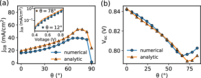
To verify the accuracy of the above expressions, we compare our analytical prediction with the results of numerical simulation. Details of the simulation software (along with its source code and a standalone executable) can be found in Ref. 3. The simulation parameters are given in Table S2 of the Supporting Information and in the caption of Fig. 4. Figure 4(a) shows a comparison of the numerically computed grain boundary recombination current (blue dots) and the analytical predictions (orange triangles) as a function of grain boundary orientation for a fixed applied voltage (). We find good agreement until the grain boundary becomes nearly completely horizontal, at which point the numerically computed current drops nearly to zero. We find that our model does not describe this full blocking configuration, however it remains accurate at .
We next consider the open-circuit voltage . Our model describes the dark forward bias current, so its applicability to relies on the superposition principle. At high forward bias, the carrier densities are large enough so that quasi-Fermi levels and the electrostatic potential have negligible differences with those in the dark. 20 Because of the high recombination rate of grain boundaries, we find that the current-voltage relation of the junction under illumination is given by the sum of the short circuit current and the dark current only near (this superposition principle does not apply in our system at lower voltages). We use the analytical model to predict by shifting the analytical dark curve by the numerically computed . Figure 4(b) shows a comparison between the resulting for analytic and numerical models as a function of grain boundary orientation. In both cases we find good agreement, demonstrating the accuracy of the analytical form for the open-circuit voltage. However we find a large discrepancy for a horizontal grain boundary , where the analytic is less than the numerical value by 0.09 V for the same reasons as the dark current discrepancy given above. We omit this data point in Fig. 4b. The general form of the open-circuit voltage can be found by setting the general form for the high-recombination grain boundary current (given in its full explicit form in Eq. (14) of the Supporting Information) equal to and solving for .
With a description of the isolated grain boundary recombination current as a function of electrical and geometrical properties, we move on to consider systems with multiple grain boundaries. It is not clear a priori that the picture of isolated grain boundary recombination is relevant to an arbitrary configuration of grain boundaries. To address this question, we first reiterate the model conditions and assumptions: 1. Grain boundaries are positively charged. 2. Grain boundaries have “high” defect density (see Supporting Information Eq. (5) for a precise criterion). 3. The hole quasi-Fermi level varies by less than . The validity of assumption 3 is the most difficult to assess. This assumption may fail as a result of poor hole transport, due to low hole mobility and/or low hole carrier concentration. For networks of grain boundaries, the wide variety of possible system geometries and parameters make it difficult to derive a precise and general set of criteria for the validity of assumption 3 and the applicability of the analytical model. In lieu of such a criterion, we numerically explore parameter space to explicitly find the domain of parameter values for which the analytical model applies.
We consider a system with 3 grain boundaries as depicted in the insets of Fig. 5. The defect energy levels of grain boundary 1, 2, and 3 lead to downward band bending values of , respectively (see inset of Fig. 5(c) for grain boundary labels). Fig. (5) provides a comparison of the analytical model with the numerical simulations as a function of hole mobility and hole doping for three different grain sizes (fixed by system size ). We choose these three parameters because they most strongly determine the applicability of the analytical model. We plot the ratio of the analytically predicted to numerically computed dark current at a fixed forward bias voltage . The red lines delimit the region in parameter space for which the ratio is greater/less than . We find that dark current ratio values of less than 2.7 correspond to systems for which the analytically predicted deviates from the numerically simulation value by less than the thermal voltage (see Fig. S1 of the Supporting Information). As expected, the factors which limit hole transport: low hole mobility and/or low hole carrier concentration due to low hole doping or depleted grains (i.e. grains smaller than the grain boundary depletion width) cause the analytical model to fail. However we find that the analytical model accurately describes the numerical simulation for a wide range of system parameters.
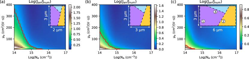
The precise limits of parameter space for which our analytical model applies depends on the details of the grain boundary geometry and defect parameters. For example, if we reduce the electrostatic band bending of grain boundary 1 from 0.71 eV to 0.21 eV, then we find the region of analytic model applicability increases slightly (see Fig. S2 of the Supporting Information). This can be expected: a decreased grain boundary built-in potential decreases the depletion width surrounding the grain boundary, so that hole carriers are less depleted and our assumption of facile hole transport is more easily satisfied. However, we find that the boundaries presented in Fig. 5 give a fairly representative indication of the analytical model’s domain of validity. We note that for a grain size of , the analytical model can be applied for parameters typical of CdTe absorbers: and .
We consider the behavior of a specific system in more detail in Fig. 6. For this simulation we use default parameter values (, ). We first show the field lines of the hole currents in Fig. 6a. When the hole currents transverse to both sides of the grain boundary core are equal and opposite (see ), the transverse hole current vanishes at the grain boundary core. For , only one side of the grain boundaries has direct access to the -contact. In this case, hole currents can partially go through grain boundaries, as seen around the left grain boundary. A fraction of the incoming holes recombine at the grain boundary core, so that hole currents on both sides are not equal. Not surprisingly, holes that did not recombine are then attracted preferentially to the grain boundary with the highest surface recombination velocity (“high S” on Figure 6a).
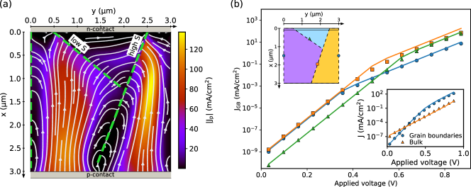
In Figure 6, we plot the numerically computed recombination current of the three grain boundaries separately (symbols), together with the analytical predictions (solid lines). In this case, the analytical theory overestimates the numerically computed current by approximately a factor of 2 at high applied voltage. At low applied voltages, all grain boundaries are either -type or -type, with ideality factor of 1. The transition to the high-recombination regime is revealed by the change of slope, corresponding to an ideality factor of 2. The lower inset of Figure 6b compares the total grain boundary and bulk recombination currents (the latter was computed in Ref. 1). In addition to its larger amplitude, the grain boundary’s recombination current exhibits change of slope. For most of the applied voltages, the bulk recombination is proportional to as given by the junction depletion region recombination. 1 Because of the variety of grain boundary properties in our geometry, the grain boundary most dominating the dark current changes with applied voltage leading to multiple changes of slope between and . This feature distinguishes grain boundary recombination from junction depletion region recombination.
Having established the conditions for which the analytical model describes the behavior of multi-grain boundary systems, we proceed with an analysis of the impact of grain boundary inhomogeneities on the open-circuit voltage using the analytical model alone. We consider an ensemble of “samples”, each with its own distributions of grain size, grain boundary orientation, gap state configuration and surface recombination velocity. For a probability distribution of the random parameter with mean and standard deviation , the average grain boundary dark current reads
| (6) |
and the open-circuit voltage is found by solving .
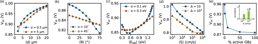
Assuming equal short-circuit currents among all “samples”, Figure 7 shows the open-circuit voltage as a function of the mean of the distribution of a grain/grain boundary property. Note that a discussion on the device efficiency, which is beyond the scope of this work, should also include the impact of grain boundary properties on . The integral Equation (6) was computed numerically with the general form for given by Equation (1). We used Gaussian distributions for Figure 7a,b,c, with small (lines with dots) and large (lines with triangles) deviations from the distribution mean. Because surface recombination velocities vary by orders of magnitude, we chose a uniform distribution over the interval for Figure 7d,e, where is the geometric deviation of the distribution. Wide (narrow) distributions represent strong (low) inhomogeneities in the grain/grain boundary property.
varies logarithmically with grain size as shown by the dots in Figure 7a, so only large variations produce significant change in the open-circuit voltage. The weak influence of grain size on open-circuit voltage was observed with photoluminescence measurement on CdTe solar cells. 21 Figure 7b shows that grain boundaries forming low angles with the normal to the junction are always more favorable, almost regardless of the inhomogeneities. The reduction of open-circuit voltage at large angles results from the increase of the length of the recombination region as shown by Equation (4). The gain of approximately in (around 5 % increase in typical values of in CdTe) encourages the engineering of a material growth process that increases the proportion of quasi-perfectly columnar grains. Efforts in this direction have been reported. 22, 23
Figure 7c shows that gap state neutral points close to a band edge generally give better than midgap values. Note that the grain boundary built-in potential attracts photogenerated electrons to the grain boundary core, resulting in enhanced recombination when holes are majority carriers there. The short circuit current is therefore more reduced by -type than -type grain boundaries (see Supporting Information), which Figure 7c does not show. Thus, only high values of built-in potential (i.e., ) are favorable for the open-circuit voltage. Experimentally, the neutral point of the gap state distribution determines the amplitude of the grain boundary built-in potential . At thermal equilibrium and in the limit of high defect density of states, this relation reads ( is the bulk Fermi energy). Increasing the spread of results in more gap state neutral levels around midgap. The probability to access midgap states being similar for both electrons and holes, such states provide higher recombination currents than states near the band edge, hence further reducing . These results are consistent with the observation that the standard CdCl2 treatment of CdTe increases the built-in potential around grain boundaries, 24 possibly leading to majority carrier type inversion under suitable conditions. 25, 26
The reduction of the open-circuit voltage by the recombination strength is quantified in Figure 7d,e, where is the effective surface recombination velocity. We observe the expected logarithmic dependence of on recombination velocity in Figure 7d. The highest surface recombination velocities of the two distributions considered in the figure differ by a factor 10. This is consistent with the difference in of about () between the two distributions. This shows that the largest value of surface recombination velocity in the sample determines . Note that because we only allow recombination velocities below the thermal velocity, saturates for in the case of . The control of the open-circuit voltage by the most deleterious grain boundaries is further illustrated in Figure 7e. A cathodoluminescence study of CdTe grain boundaries revealed that approximately of the boundaries were active recombination centers. 27 Here we show that even a small proportion of active recombination centers is sufficient to degrade . We assumed a bimodal distribution of active and inactive grain boundaries with low () and high () average recombination velocities, as shown in inset. In this instance, we find that a proportion of only of active grain boundaries gives an open-circuit voltage equivalent to that of a system fully saturated with active grain boundaries. This observation is best understood by assuming that only surface recombination velocities and are present in the sample (i.e., a probability distribution with two Dirac delta functions). In this case the average surface recombination velocity across the sample is
| (7) |
where is the proportion of active grain boundaries. As and are separated by orders of magnitude, Equation (7) shows that only a small proportion of active grain boundaries (e.g., ) is sufficient to dramatically shift the average recombination velocity towards high values.
Our last observation is the resilience of to moderate inhomogeneities, a common feature among the wide parameter distributions. In the high recombination regime (most relevant around ), the dark recombination current varies only algebraically (not exponentially) with all the grain boundary parameters. In turn, the open-circuit voltage varies logarithmically with these parameters, leading to some tolerance towards variations.
In this work, new analytical results were provided for the dark recombination current of grain boundaries forming non-perfectly columnar grains. The model accounts for the main features of grain boundaries: grain size, orientation, gap state configuration and recombination strength. Generalizing the isolated grain boundary picture to networks of grain boundaries is accomplished by finding the parameter space for which contributions of grain boundary recombination can be added independently. We find that for parameters relevant for many thin film photovoltaics, this generalization is valid. Applying these results to random distributions of grain boundary properties led to practical observations regarding the open-circuit voltage. In particular, tolerates moderately heterogeneous grain boundary properties.
To our knowledge, this work is the first fully analytical, quantitative description of grain boundary networks. It contributes to bridge the gap between experimental determination of grain boundary properties and their impact on the device open-circuit voltage. The combination of this theory with nanoscale measurements and first principle calculations can lead to a comprehensive approach to improve the performance of thin-film solar cell technologies.
Supporting information
Explicit form for the analytical current-voltage relations; numerical simulations demonstrating that the analytic dark current-voltage relation accurately predicts the open-circuit voltage; additional numerical simulations demonstrating that the values of grain boundary built-in potential does not appreciably change the regime of validity for the analytical model; table of default simulation parameters
Acknowledgments
B. G. acknowledges support under the Cooperative Research Agreement between the University of Maryland and the National Institute of Standards and Technology Center for Nanoscale Science and Technology, Award 70NANB14H209, through the University of Maryland.
References
- Kumar and Rao 2014 Kumar, S. G.; Rao, K. K. Physics and Chemistry of CdTe/CdS Thin Film Heterojunction Photovoltaic Devices: Fundamental and Critical Aspects. Energy Environ. Sci. 2014, 7, 45–102
- Geisthardt et al. 2015 Geisthardt, R. M.; Topič, M.; Sites, J. R. Status and Potential of CdTe Solar-Cell Efficiency. IEEE J. Photovolt. 2015, 5, 1217–1221
- Gloeckler et al. 2013 Gloeckler, M.; Sankin, I.; Zhao, Z. CdTe Solar Cells at the Threshold to 20% Efficiency. IEEE Journal of Photovoltaics 2013, 3, 1389–1393
- Zhao et al. 2016 Zhao, Y.; Boccard, M.; Liu, S.; Becker, J.; Zhao, X.-H.; Campbell, C. M.; Suarez, E.; Lassise, M. B.; Holman, Z.; Zhang, Y.-H. Monocrystalline CdTe Solar Cells With Open-Circuit Voltage Over V and Efficiency of . Nat. Energy 2016, 1, 16067
- 5 Burst, J. M.; Duenow, J. N.; Albin, D. S.; Colegrove, E.; Reese, M. O.; Aguiar, J. A.; Jiang, C.-S.; Patel, M.; Al-Jassim, M. M.; Kuciauskas, D.; Swain, S.; Ablekim, T.; Lynn, K. G.; Metzger, W. K. CdTe Solar Cells With Open-Circuit Voltage Breaking the V Barrier. Nat. Energy 2016, 1, 16015
- Sites et al. 1998 Sites, J. R.; Granata, J.; Hiltner, J. Losses Due to Polycrystallinity in Thin-Film Solar Cells. Solar Energy Materials and Solar Cells 1998, 55, 43–50
- Major 2016 Major, J. D. Grain Boundaries in CdTe Thin Film Solar Cells: a Review. Semiconductor Science and Technology 2016, 31, 093001
- Card and Yang 1977 Card, H. C.; Yang, E. S. Electronic Processes at Grain Boundaries in Polycrystalline Semiconductors Under Optical Illumination. IEEE Trans. Electron Devices 1977, 24, 397–402
- Fossum and Lindholm 1980 Fossum, J. G.; Lindholm, F. A. Theory of Grain-Boundary and Intragrain Recombination Currents in Polysilicon pn-Junction Solar Cells. IEEE Trans. Electron Devices 1980, 27, 692–700
- Green 1996 Green, M. A. Bounds Upon Grain Boundary Effects in Minority Carrier Semiconductor Devices: A Rigorous “Perturbation” Approach With Application to Silicon Solar Cells. J. Appl. Phys. 1996, 80, 1515–1521
- Edmiston et al. 1996 Edmiston, S.; Heiser, G.; Sproul, A.; Green, M. Improved Modeling of Grain Boundary Recombination in Bulk and p-n Junction Regions of Polycrystalline Silicon Solar Cells. J. Appl. Phys. 1996, 80, 6783–6795
- Wang et al. 2011 Wang, Z.; Saito, M.; McKenna, K. P.; Gu, L.; Tsukimoto, S.; Shluger, A. L.; Ikuhara, Y. Atom-Resolved Imaging of Ordered Defect Superstructures at Individual Grain Boundaries. Nature 2011, 479, 380–383
- Sun et al. 2016 Sun, C.; Paulauskas, T.; Sen, F. G.; Lian, G.; Wang, J.; Buurma, C.; Chan, M. K. Y.; Klie, R. F.; Kim, M. J. Atomic and Electronic Structure of Lomer Dislocations at CdTe Bicrystal Interface. Sci. Rep. 2016, 6, 27009
- Yan et al. 2015 Yan, Y.; Yin, W.-J.; Wu, Y.; Shi, T.; Paudel, N. R.; Li, C.; Poplawsky, J.; Wang, Z.; Moseley, J.; Guthrey, H.; Moutinho, H.; Pennycook, S. J.; Al-Jassim, M. M. Physics of Grain Boundaries in Polycrystalline Photovoltaic Semiconductors. J. Appl. Phys. 2015, 117, 112807
- Yoon et al. 2013 Yoon, H. P.; Haney, P. M.; Ruzmetov, D.; Xu, H.; Leite, M. S.; Hamadani, B. H.; Talin, A. A.; Zhitenev, N. B. Local Electrical Characterization of Cadmium Telluride Solar Cells Using Low-Energy Electron Beam. Sol. Energ. Mat. Sol. Cells 2013, 117, 499–504
- Jiang et al. 2004 Jiang, C.-S.; Noufi, R.; AbuShama, J. A.; Ramanathan, K.; Moutinho, H. R.; Pankow, J.; Al-Jassim, M. M. Local Built-In Potential on Grain Boundary of Cu(In,Ga)Se2 Thin Films. Appl. Phys. Lett. 2004, 84, 3477–3479
- Gaury and Haney 2016 Gaury, B.; Haney, P. M. Charged Grain Boundaries Reduce the Open-Circuit Voltage of Polycrystalline Solar Cells–An Analytical Description. J. Appl. Phys. 2016, 120, 234503
- Gaury and Haney 2017 Gaury, B.; Haney, P. M. Charged Grain Boundaries and Carrier Recombination in Polycrystalline Thin-Film Solar Cells. Physical Review Applied 2017, 8, 054026
- Gaury et al. 2018 Gaury, B.; Sun, Y.; Bermel, P.; Haney, P. M. Sesame: a 2-Dimensional Solar Cell Modeling Rool. arXiv preprint arXiv:1806.06919 2018,
- Tarr and Pulfrey 1980 Tarr, N. G.; Pulfrey, D. L. The Superposition Principle for Homojunction Solar Cells. IEEE Trans. on Electron Devices 1980, 27, 771–776
- Metzger et al. 2003 Metzger, W. K.; Albin, D.; Levi, D.; Sheldon, P.; Li, X.; Keyes, B. M.; Ahrenkiel, R. K. Time-Resolved Photoluminescence Studies of CdTe Solar Cells. J. Appl. Phys. 2003, 94, 3549–3555
- Luschitz et al. 2009 Luschitz, J.; Siepchen, B.; Schaffner, J.; Lakus-Wollny, K.; Haindl, G.; Klein, A.; Jaegermann, W. CdTe Thin Film Solar Cells: Interrelation of Nucleation, Structure, and Performance. Thin Solid Films 2009, 517, 2125 – 2131
- Spalatu et al. 2015 Spalatu, N.; Hiie, J.; Mikli, V.; Krunks, M.; Valdna, V.; Maticiuc, N.; Raadik, T.; Caraman, M. Effect of CdCl2 Annealing Treatment on Structural and Optoelectronic Properties of Close Spaced Sublimation CdTe/CdS Thin Film Solar Cells vs Deposition Conditions. Thin Solid Films 2015, 582, 128 – 133
- Tuteja et al. 2016 Tuteja, M.; Koirala, P.; Palekis, V.; MacLaren, S.; Ferekides, C. S.; Collins, R. W.; Rockett, A. A. Direct Observation of CdCl2 Treatment Induced Grain Boundary Carrier Depletion in CdTe Solar Cells Using Scanning Probe Microwave Reflectivity Based Capacitance Measurements. J. Phys. Chem. C 2016, 120, 7020–7024
- Li et al. 2014 Li, C.; Wu, Y.; Poplawsky, J.; Pennycook, T. J.; Paudel, N.; Yin, W.; Haigh, S. J.; Oxley, M. P.; Lupini, A. R.; Al-Jassim, M.; Pennycook, S. J.; Yan, Y. Grain-Boundary-Enhanced Carrier Collection in CdTe Solar Cells. Phys. Rev. Lett. 2014, 112, 156103
- Kranz et al. 2014 Kranz, L.; Gretener, C.; Perrenoud, J.; Jaeger, D.; Gerstl, S. S. A.; Schmitt, R.; Buecheler, S.; Tiwari, A. N. Tailoring Impurity Distribution in Polycrystalline CdTe Solar Cells for Enhanced Minority Carrier Lifetime. Advanced Energy Materials 2014, 4, 1301400–n/a, 1301400
- Moseley et al. 2015 Moseley, J.; Metzger, W. K.; Moutinho, H. R.; Paudel, N.; Guthrey, H. L.; Yan, Y.; Ahrenkiel, R. K.; Al-Jassim, M. M. Recombination by Grain-Boundary Type in CdTe. J. Appl. Phys. 2015, 118, 025702
Supporting information
| Param. | -type | -type | high-recombination | ||||
|---|---|---|---|---|---|---|---|
| n | |||||||
| N | |||||||
| S | |||||||
|
|
|
We use the model for charged grain boundaries of Ref. 1, which is summarized here. A single grain boundary is modeled as a two-dimensional plane with a donor and acceptor gap states at equal energy . This is a convenient model that exhibits Fermi level pinning at a charge neutrality level 4. The corresponding grain boundary charge density reads
| (8) |
where is a two-dimensional defect density. The defect state occupancy is 5:
| (9) |
where () is the grain boundary electron (hole) carrier density, () is the electron (hole) surface recombination velocity, and are given by:
| (10) | ||||
| (11) |
where is a defect energy level calculated from the valence band edge, () is the conduction (valence) band effective density of states, is the material bandgap, is the Boltzmann constant and is the temperature. The parameters and are related to the electron and hole capture cross sections by , where is the thermal velocity. In the present work we varied with fixed ; this corresponds to varying accordingly.
We consider large defect densities of states such that the Fermi level is pinned near the defect energy level (which is the charge neutrality level for this model). This regime was found to be reached for densities above the critical value
| (12) |
where is the equilibrium Fermi energy and is the doping density. For default material parameters and grain boundary band bending of , is typically on the order of .
The diffusion length for electrons confined near the grain boundary depends on grain boundary type. We denote this with and for -type and high-recombination grain boundary, respectively. The relevant expressions are given below:
| (13) | |||||
| (14) |
where
| (15) | |||||
| (16) |
where . is the length scale associated with the transverse electric field of the grain boundary in the high recombination regime: . In Eq. 15, is the equilibrium potential difference between grain boundary and grain interior.
We next provide the general expressions for the recombination current of -type and high recombination grain boundaries (the expressions in the main text only show limiting values of and . For -type, the recombination is given by:
| (17) |
As described in the main text, is the position where in equilibrium. Its expression is:
| (18) |
where is the bulk depletion width, and is the potential difference of the bulk - junction:
| (19) | |||||
| (20) |
For high-recombination, the recombination is given by:
| (21) |
We have also checked that grain boundary networks with more complex defect electronic structure, such as a continuum of donors and acceptors (as described in Ref. 2), are accurately described by the approach we present here.
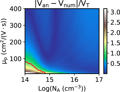
Figure 8 shows that the reliability of the analytical model’s prediction for tracks its reliability for dark . The red line indicating the region for which the analytical model predicts the numerically computed is similar to the region for which the analytical model predicts the numerically computed dark current to within a factor of (see Fig. 5b).
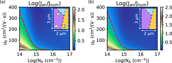
Figure 9 shows the dependence of the analytical model performance on the grain boundary built-in potential. We find that this parameter does not strongly influence the model reliability. In general, the smaller the grain boundary built-in potential, the larger the regime of applicability, although the difference is quite small.
We tested our analytical predictions on numerical solutions of the two-dimensional drift-diffusion-Poisson equations, solved using Sesame3. We used selective contacts, so the hole (electron) current vanishes at (). Periodic boundary conditions were applied in the -direction. Table 2 gives a list of the material parameters used in these calculations.
| Param. | Value | Param. | Value |
|---|---|---|---|
References
- Gaury and Haney 2016 Gaury, B.; Haney, P. M. Charged Grain Boundaries Reduce the Open-Circuit Voltage of Polycrystalline Solar Cells–An Analytical Description. J. Appl. Phys. 2016, 120, 234503
- Gaury and Haney 2017 Gaury, B.; Haney, P. M. Charged Grain Boundaries and Carrier Recombination in Polycrystalline Thin-Film Solar Cells. Physical Review Applied 2017, 8, 054026
- Gaury et al. 2018 Gaury, B.; Sun, Y.; Bermel, P.; Haney, P. M. Sesame: a 2-Dimensional Solar Cell Modeling Rool. arXiv preprint arXiv:1806.06919 2018,
- Taretto and Rau 2008 Taretto, K.; Rau, U. Numerical Simulation of Carrier Collection and Recombination at Grain Boundaries in Cu(In,Ga)Se2 Solar Cells. J. Appl. Phys. 2008, 103, 094523
- Shockley and Read 1952 Shockley, W.; Read, W. T. Statistics of the Recombinations of Holes and Electrons. Phys. Rev. 1952, 87, 835–842