Magnetism and structure of in-situ grown FeN films studied using N K-edge XAS and nuclear resonance scattering
Abstract
We studied the structural and magnetic properties of in-situ grown iron mononitride (FeN) thin films. Initial stages of film growth were trapped utilizing synchrotron based soft x-ray absorption near edge spectroscopy (XANES) at the N -edge and nuclear resonant scattering (NRS). Films were grown using dc-magnetron sputtering, separately at the experimental stations of SXAS beamline (BL01, Indus 2) and NRS beamline (P01, Petra III). It was found that the initial stages of film growth differs from the bulk of it. Ultrathin FeN films, exhibited larger energy separation between the t2g and eg features and an intense eg feature in the N -edge pattern. This indicates that a structural transition is taking place from the rock-slat (RS)-type FeN to zinc-blende(ZB)-type FeN when the thickness of films increases beyond 5 nm. The behavior of such N -edge features correlates very well with the emergence of a magnetic component appearing in the NRS pattern at 100 K in ultrathin FeN films. Combining the in-situ XANES and NRS measurements, it appears that initial FeN layers grow in RS-type structure having a magnetic ground state. Subsequently, the structure changes to ZB-type which is known to be non-magnetic. Observed results help in resolving the long standing debate about the structure and the magnetic ground state of FeN.
I Introduction
Iron and nitrogen are among the most abundant elements on the earth and therefore iron-nitrogen compounds - FeNx, are not only economical but also also environment friendly. They are being investigated for applications in a variety of fields. For x 0.5 in FeNx, compounds formed are magnetic and have been explored for applications as rare earth free permanent magnets, spintronic materials and also other emerging magnetic devices Bhattacharyya_FeN_Review . At x = 0.12 (in FeNx), the phase formed is , which has been long debated to possess a giant magnetic moment, M3/Fe atom 2000_JMMM_Fe16N2_gmm_or_not and is still being a subject of intense research 2016_Sci_Rep_Fe16N2 . At x = 0.25 the phase formed is which is predicted to have almost 100 spin polarization ratio and a half-metallic character 2006_PRB_Fe4N_SPR , its larger (than Fe) M 2.5/Fe atom JMMM10_Matar ; APL11_Ito_Fe4N ; 2009_PSS_B_Fe4N_th_exp_Blanca makes it a suitable candidate in spintronic devices and a potential alternative to Heusler alloys 2018_APL_Fe4N_underlayer . Between x = 0.33 to 0.5 in FeNx, phases formed are (0 y 1), they are thermally stable and possess soft-magnetic properties 2016_JAC_Fe3N_soft_mag and recently exhibited for usage in Li-ion batteries 2017_nano_energy_Fe3N_li-on_battery . At x = 0.5, the phase forms Cai_2000 which has been used as a precursor to produce iron mononitride (FeN) and iron pernitride (FeN2) by application of high-pressure and high-temperature (HPHT) 2018_inorgchem_FeN2 .
N rich phases of iron-nitrogen compounds (x in FeNx) were theoretically predicted for a while, e.g. the spinel nitride Fe3N4 Fe3N4:JAP02 ; 2002_APL_Fe3N4 and the pernitride FeN2 2011_Chemistry_FeN2_prediction , only very recently the FeN2 phase has been synthesized experimentally under HPHT (T2000 K, P50 GPa) 2018_inorgchem_FeN2 ; 2018_Nat_Com_poly_FeNx and by raising the pressure above 100 GPa, the FeN4 phase was also evidenced by Bykov et al. 2018_Nat_Com_poly_FeNx . Very recently even higher N phases like FeN6 and FeN8 have been predicted 2018_Chemistry_Materials_polyN_FeN_theory . Polymeric nitrogen chains present in N rich FeNx compounds makes them very attractive as high energy density materials (HEDMs), however their synthesis under ambient temperature and pressure remains a challenge.
While magnetic FeNx compounds already started to get attention in early 1950s Jack1951 , experimental works on the mononitride phase can only be traced back in last three decades or so Oueldennaoua.SM.1985 ; Nakagawa.HypInt.1991 ; Suzuki.JAC1993 ; 1997_PhysicaB_Hinomura . FeN compounds were extensively studied by Schaff et al. SchaafHypInt95 ; Niederdrenk_JAC96 ; Rissanen_JAC98 ; Schaaf.PMS.2002 in late 1990s. Subsequently, FeN thin films were synthesized using ion beam sputtering 2001_Vacuum_MG_FeN_IBS , dc/rf magnetron sputtering 2003_ASS_FeN_dcMS ; 2004_JAC_FeN_plasma_gas_cond ; Gupta:PRB05 ; 2006_TSF_FeN_TEM_Demange ; Jouanny2010TSF ; gupta:JAP2011 ; MG:JAC:2011 ; 2015:PRB:MG:FeN ; 2015_JAC_FeAlN_MG ; 2017_Mat_today_FeN_dcMS ; 2019_JMMM_Fe4N_by_FeN , pulsed laser deposition (PLD) Gupta_JAC01 ; 2005_MSE_B_Laser_Nitriding ; 2012_HI_FeN_PLD ; 2013_HI_FeN_PLD , high power impulse magnetron sputtering SCT15_Akhil , nitrogen plasma assisted molecular beam epitaxy (MBE) Navio.PRB08 ; 2003_HI_Borsa ; 2006_NIMB_stoichiometic_FeN ; JPak_2010 ; JCG15_FeN_MBE_Naito and very recently under HPHT 2018_inorgchem_FeN2 ; 2018_Nat_Com_poly_FeNx ; 2017_Iorg_Chem_FeN_FeN2 ; 2018_JAC_FeN_megabar ; 2017_Angew_Chem_NiAs_FeN . From applications points of view, the mononitride FeN is also very interesting as its oxidation resistance makes it a effective catalyst in chemical reactions 2006_Cat_Comm_FeN_Catalysis ; 2011_EES_FeN_Catalyst , it can be used as precursor to yield magnetic phases in a controlled way 2019_JMMM_Fe4N_by_FeN ; Navio.PRB08 ; Navio:APL:2009 ; Navio.NJP2010 and also in biomedical applications 2018_Chemistry_Materials_polyN_FeN_theory . However, the fundamental understanding of mononitride FeN compound is still not well understood and variances can be seen between theory and experiments in terms of the lattice parameter (LP), structure and the magnetic ground state.
Considering recent theoretical works 2018_Chemistry_Materials_polyN_FeN_theory ; 2019_JAC_FeN_1st_pricipal ; 2017_JPCS_FeN_CoN_DFT ; 2015_RSC_ADV_mag_order ; 2014_JAC_3d_mononitride_1st_princ ; 2012_JAC_Soni ; FeN:PRB:Houari and comparing with experimental works, various possibilities emerge about the structure and the magnetic ground state of FeN (i) -FeN with zinc-blende (ZB)-type structure (LP4.3 Å) and a nonmagnetic (NM) ground state (ii) -FeN with rock-salt (RS)-type structure (LP4.5 Å) and a ferromagnetic (FM) or antiferromagnetic (AFM) ground state (iii) NiAs-type structure with a FM ground state (iv) CsCl-type structure with NM ground state (iv) wurtzite-type structure with a NM ground state (v) MnP-type structure at very high pressure. Among these, FeN in CsCl, wurtzite and MnP structures has not yet been synthesized experimentally, NiAs-type structure was experientially evidenced recently under HPHT 2018_inorgchem_FeN2 ; 2018_Nat_Com_poly_FeNx ; 2017_Iorg_Chem_FeN_FeN2 ; 2018_JAC_FeN_megabar ; 2017_Angew_Chem_NiAs_FeN . Under ambient temperature and pressure conditions only the ZB and RS-type FeN have been evidenced hitherto, however the existence of RS-type FeN is still debated experimentally. Recent first-principles calculations carried out by Li et al. 2019_JAC_FeN_1st_pricipal predict that the total energy for ZB-FeN (non spin polarized) at -16.893 eV is only slightly lower than for RS-FeN (spin polarized) at -16.892 eV. This energy is significantly higher for all other FeN phases mentioned above. Therefore, at T = 0 K and P = 0 GPa, the preferred phase is ZB-type FeN followed by RS-type FeN.
From a review of recent experimental works probing the magnetic ground state of FeN, it can be seen that irrespective of its LP (4.3 or 4.5 Å), FeN remains non-magnetic down to 2 K. An exception to this, are studies peformed by Usui and Yamada 2012_HI_FeN_PLD ; 2013_HI_FeN_PLD and earlier works of Nakagawa Nakagawa.HypInt.1991 , Suzuki Suzuki.JAC1993 and Hinomura 1997_PhysicaB_Hinomura et al. In all these works a magnetic phase was found at low temperature but along with an oxide phase. Usui and Yamada 2012_HI_FeN_PLD ; 2013_HI_FeN_PLD deposited FeN films using PLD and by varying the nitrogen partial pressure they synthesized ZB-type -FeN and RS-type -FeN. In these works low temperature (down to 5 K) 57Fe Mössbauer spectroscopy measurements were carried out and it was concluded that -FeN remain NM and -FeN become AFM at low temperature. The Néel temperature () estimated for -FeN films was 220 K. In addition to the AFM component with a hyperfine field of about 30 T an additional component with hyperfine field of 49 T was also observed. Generally, such component stems from an oxide phase Nakagawa.HypInt.1991 ; 1997_PhysicaB_Hinomura therefore, the purity of these samples was questionable.
Jouanny et al. Jouanny2010TSF prepared FeN thin films having LP 4.5 Å using sputtering at 373 K and from their zero-field-cooled and field-cooled (1 T) magnetization measurements they could not find the presence of any magnetic order. J. Pak et al. JPak_2010 studied the growth behavior of epitaxial FeN thin films deposited using N plasma assisted MBE and from their in-situ reflection high energy electron diffraction (RHEED) measurements they found that the LP of ultrathin FeN films was about 4.52 Å. Up to about 53 monolayers (ML), the LP of FeN films remained at this value but for a 140 ML thick (60 nm) FeN film, the LP reduced to 4.32 Å. This reduction in LP was explained in terms of an intrinsic in-plane tensile stress that generates during the growth of the film. They also did magnetization and susceptibility measurements on the 60 nm thick sample down to 5 K and could not find the presence of any magnetic order. Gupta et al. MG:JAC:2011 prepared FeN films with LP4.5 Å using sputtering at 300 K and did 57Fe Mössbauer spectroscopy measurements down to 5 K and could not find any magnetic ordering even after applying a magnetic field of 5 T. It may be noted that the LP of FeN films seems to vary with the growth temperature (), when 400 K, LP 4.5 Å and between 400-500 K its was LP4.3 K.
Above experimental results indicate that ultrathin FeN films may behave differently than their thicker counterparts. When the growth of FeN films starts their LP is large and an intrinsic in-plane tensile stress forces it to reduce. In such a situation it can be assumed that initial FeN layer grow with a RS-type motif which changes to ZB-type when film thickness increases beyond a critical value. This critical thickness can be changed by varying the deposition conditions. However, to prove this point, low temperature magnetic measurements needs to be done on ultrathin films, preferably during in-situ growth to avoid surface contamination. Hitherto, low temperature magnetization measurements were performed only on thick FeN films ( 50 nm).
Magnetization and structural measurements at low temperatures on ultrathin films combined with in-situ thin film growth is a challenging task. In the present work we achieved this by preparing in-situ systems capable of doing x-ray absorption near edge spectroscopy (XANES) measurements at N -edge and nuclear resonant scattering (NRS) measurements. It is known that N -edge XANES can provide reliable information about the coordination between metal and N atoms 1997_SSR_JG_Chen_Review and NRS is a technique which is analogues to Mössbauer spectroscopy thereby providing the information about the local magnetic structure 1996_HI_Ruffer_NRS . In both cases FeN films were grown using a similar magnetron sputtering source (1 inch) and under similar deposition conditions. From N -edge XANES measurements, we observed a structural transition taking place between 5-10 nm and low temperature (100 K) NRS measurements also exhibited the presence of a magnetic component at similar thicknesses. These first ever in-situ N -edge and NRS measurements clearly reveal that ultrathin FeN films grow in the RS-type structure and are magnetic at 100 K. When the thickness of FeN film increases beyond few nm, the structure changes to ZB-type FeN which has a non-magnetic ground state.
II Experimental
In order to study the early stages of film growth, a magnetron sputtering system was mounted separately at the soft x-ray absorption spectroscopy (SXAS) beamline BL01 XAS_beamline of Indus 2 synchrotron radiation (SR) source at RRCAT, Indore, India and at the NRS beamline P01 p01c of Petra III SR radiation source at DESY, Hamburg, Germany. In both cases a 1 inch magnetron source (AJA Int. Inc.) with Fe or 57Fe target was used and keeping experimental conditions similar, FeN films of thickness ranging from sub nm to few tens of nm were deposited. Nitrogen alone was used to sputter the iron target. By using nitrogen alone as the sputtering medium (instead of a mixture of Ar+N2), single phase FeN films can be synthesized in reactive dc magnetron sputtering(dcMS) Nakagawa.HypInt.1991 ; MG:JAC:2011 ; 2015:PRB:MG:FeN ; 2019_JMMM_Fe4N_by_FeN . After growing a film of a particular thickness, XANES or NRS measurements were performed. Prior to in-situ experiments, few test samples were deposited to determine the deposition rates (using x-ray reflectivity), the crystalline structure using x-ray diffraction (XRD, Bruker D8 Advance using Cu- x-rays) and the magnetic structure using room temperature conversion electron Mössbauer spectroscopy (CEMS). The details of the experimental stations exclusively prepared in this work are described below.
II.1 In-situ system at SXAS beamline
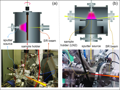
In the ultra-high vacuum (UHV) experimental station of SXAS beamline, a magnetron sputtering source was installed. This source was mounted as shown in the schematic diagram in fig. 1 (a). A photograph of the experimental chamber with the sputter source is also shown in fig. 1 (a). Using this source FeN films were deposited on a Si substrate facing the source and then the substrate was rotated along its axis so as to allow the SR x-rays to fall directly on to the deposited sample. A mass flow controller was also mounted to control the gas flow precisely. Using N2 (purity 99.9995%) alone as the sputtering medium, an iron target (purity 99.995%) - 1 inch and thickness 0.5 mm was sputtered. The base pressure in the vacuum chamber was about 210-8 mbar and with N2 gas flowing at about 20 sccm, the pressure during deposition was about 510-3 mbar.
The sputter source was equipped with a shutter so that the actual film deposition can be started after stabilizing the source conditions. Prior to in-situ experiments, Fe target was pre-sputtered to remove surface contaminations. The sputtering power used was about 15 W (450 V dc) and the target - substrate distance was about 5 cm. All samples were deposited at ambient temperature without any intentional heating on a clean Si substrate. After each deposition the chamber was evacuated back to UHV conditions and XANES measurements at the N -edges were carried out in the total electron yield mode. Typically, a N -edge scan takes about a couple of minutes and a number of scans were averaged to improve the data reliability and statistics. The energy resolution at the N -edge is better than 0.2 eV. The effectiveness of such in-situ growth using SXAS has been amply demonstrated during the growth of Cr 2010_JAC_Cr_XAS_insitu , TiO2 2014_BJN_TiO2_insitu_XAS , TiN 2017_AIP_TiN_RG and very recently for Fe films on MgO 2019_JPCM_Fe_insitu .
II.2 In-situ system at NRS beamline
Similarly for in-situ NRS measurements also a 1 inch MS source was installed in a vacuum chamber as shown in the schematic diagram and photograph in fig.1 (b). Here instead of natural Fe, a 57Fe target with about 95% abundance and 99.95% purity was used. The thickness of this target was 0.4 mm. The sample holder was either held at ambient temperature (300 K) or cooled with liquid nitrogen (LN2) flowing continuously in the copper reservoir holder. The temperature achieved at the substrate surface was about 100 K. The base pressure achieved in the chamber was about 310-8 mbar (after a bake out). All other deposition conditions were kept similar as described in section II.1. Samples were deposited on a sapphire substrate.
Here also after depositing a film, the chamber was evacuated again to UHV conditions and then NRS and x-ray (electronic) reflectivity (XRR) was measured. Since both NRS and XRR measurements can be done, almost simultaneously (one after the other within few minutes), the information about the magnetic structure and sample thickness, density, roughness etc. can be obtained in a unique way. The SR beam was tuned to 57Fe nuclear resonance energy of 14.4 keV. Utilizing the pulse structure of SR beam, the prompt scattering taking place within few ns was used to record the XRR pattern, in the -2 mode and NRS was recorded using a multi channel analyzer between 5 to 150 ns in the forward scattering geometry. The angle of incidence during NRS measurements was just above the critical angle. The details of the beamline can be in found in p01c ; wille2010NFS and about the NRS of SR in 1996_HI_Ruffer_NRS ; 2013_Kai_NRS ; 1996_HI_Smirnov_NRS_SR ; 2008_CRP_NRS_Ruffer ; Ralf_NRS .
III Results and Discussion
III.1 Structural and magnetic characterization of FeN thin film
Prior to in-situ experiments, preliminary characterization of a 50 nm thick FeN samples was carried out to understand its structural and magnetic properties. Shown in fig.2 (a) is the XRD pattern of this sample exhibiting a broad peak around 2 = 34.9∘ with a grain size of about 12.5(0.5) nm. This peak can be assigned to FeN(111) and the LP comes out to be 4.45 Å. Generally, the LP of FeN films has been found anywhere between 4.3 to 4.55 Å and when FeN films are deposited at low ( 400 K), LP 4.5 Å Jouanny2010TSF ; MG:JAC:2011 ; Naito:FeN:14 and at high , LP reduces to about 4.3 Å JPak_2010 ; Naito:FeN:14 . Therefore, from our XRD measurements, we can confirm the formation of mononitride FeN phase.
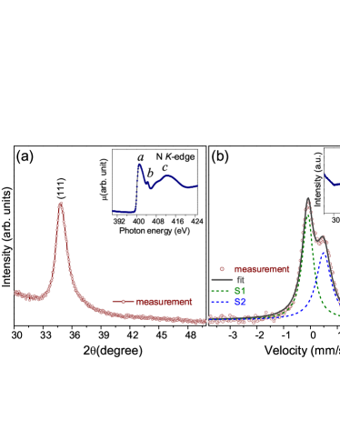
The N -edge XANES pattern of this test sample is shown in the inset fig.2 (a). Here, prominent features are labelled as , and . Here and correspond to transition from N 1 to hybridized states of Fe 3 and N 2. Features and can be assigned as t2g and eg in the octahedral and e and t2 in the tetrahedral symmetry as explained later in section III.3. Higher energy feature is due to electronic transition from N1 to a hybridized N2 and Fe4 states 1997_SSR_JG_Chen_Review . Although N -edge XANES has been used as a finger print to identify the electronic structure of early transition metal nitrides, such measurements in FeN system are almost nonexistent. In our recent work, we found that the intensity of feature becomes almost negligible (compared to feature ) 2015:PRB:MG:FeN in 150-200 nm thick FeN films deposited at 300 K. Generally, in octahedral symmetry both and features are clearly resolved e.g. in case of TiN 1993_JESRP_SORIANO_TiN_XAS and CrN 2004_SSC_N_K_edge_CrN_C2N ; 2019_TSF_CrN_MG . In fact N -edge features have been compared in fcc CrN and hcp Cr2N and it was anticipated that due to octahedral crystal field, N -edge features show splitting in CrN but in Cr2N, no such splinting can be seen in absence of octahedral crystal field 2004_SSC_N_K_edge_CrN_C2N . Therefore, N -edge XANES can be used to distinguish between ZB and RS-type FeN, as demonstrated from our in-situ measurements presented in section III.3.
The magnetic state of another test sample (50 nm 57FeN film) was measured using CEMS as shown in fig. 2 (b). It shows an asymmetric peak typically found in FeN films. This peak was deconvoluted into two singlets - S1 and S2. We find that the isomer shift of S1 is around 0, while that of S2 0.5 mm/s. Here, S1 can be assigned to Fe coordinated with four N atoms as expected in ZB-type FeN; S2 can be understood to originate due to various factors such as defects or vacancies in ZB-FeN in agreement with previous works MG:JAC:2011 ; Jouanny2010TSF ; 2006_NIMB_stoichiometic_FeN ; 2003_HI_Borsa . The NFS pattern of this sample is shown in the inset of fig. 2 (b). The featureless pattern confirms that this sample is non-magnetic. Details of NFS results are discussed in section III.4. Therefore, our 50 nm sample can be assigned as non-magnetic FeN (at 300 K) having a ZB-type structure with a LP of 4.45 Å.
III.2 In-situ NRS measurements at 300 K
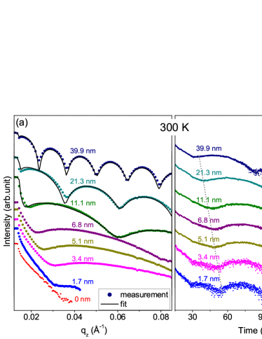
Figure 3(a,b) shows the XRR and NRS patterns taken during in-situ deposition of 57FeN thin film for various film thicknesses. As films become thick, the frequency of oscillation increases in the XRR pattern signifying that the thickness of films is increasing. The fitting of XRR pattern reveal that film roughness is within 1-2 nm and estimated film density matches well with FeN films. The NRS pattern of all FeN films show broad oscillations - marked by a dashed line as shown in fig. 3(b). These broad oscillations arise due to thickness of the film and are known as dynamical beats, explained in section III.4. The absence of beating patterns arising due to hyperfine interactions (electric quadrupole or magnetic dipole) signifies that all FeN films are non-magnetic, irrespective of film thickness. Only the thinnest sample (1.7 nm) shows an additional beat which could have magnetic origin but due to low thickness and poor statistics, it is difficult to assign any magnetic component. FeN films at 300 K are expected to be non-magnetic. They might show a magnetic signature when cooled below 220 K 2013_HI_FeN_PLD . Therefore, our 300 K in-situ measurements demonstrate the capability of the technique to probe ultrathin films. In order to probe the magnetic ground state we did in-situ XRR and NRS measurements at 100 K which are presented in section III.4.
III.3 In-situ N -edge XANES measurements
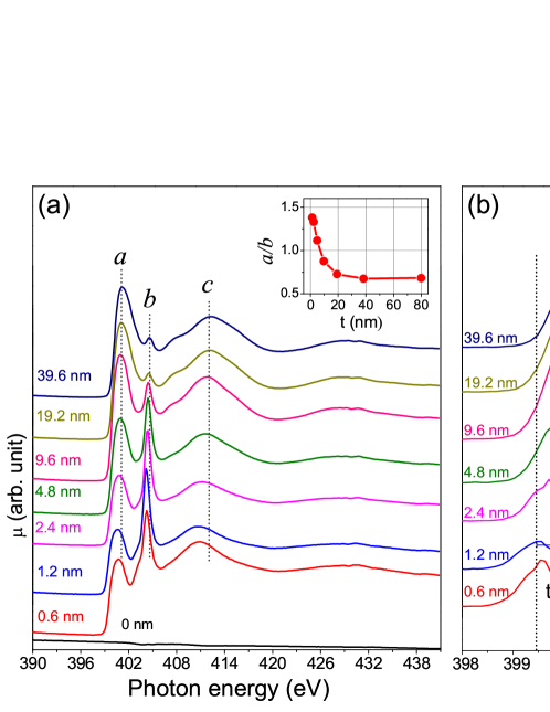
Figure 4 shows the N -edge XANES patterns taken during the in-situ growth of FeN films at 300 K. Before starting the deposition, the chamber was flushed with N2 gas 2-3 times and after evacuating the chamber to UHV conditions, N -edge measurements were performed on the bare substrate. As expected no signatures of N -edge features can be seen on the bare substrate. Subsequently FeN film was deposited for a short time and it was astonishing to see that prominent N -edge features can be seen even when film thickness was less than a monolayer (not shown) and for a 0.6 nm film, well-resolved N -edge features can be seen in fig. 4(a). The assignment of these features as , and was already explained in sec. III.1. Shown in fig. 4(b) is a magnified view of the derivative of absorption coefficient (d/dE) depicting the precise positions of features and . For ultrathin films ( 5 nm), we can see that the feature is the strongest, also it shows a shoulder on the lower energy side (marked by an arrow in fig. 4(b)), which could be due to some splitting in the e orbitals.
When the film thickness increases to 9.6 nm, this shoulder disappears and the feature suddenly becomes the weakest. For films of even higher thickness the feature becomes even smaller (than both and ). The ratio of features and is plotted in the inset of fig. 4(a). Another prominent change that can be clearly seen is the shift in the position of features and . We can see that both and shift to higher energy as thickness increases and the energy difference of these two features () reduces from 4.4 eV to 4.1 eV when the thickness increases from 1.2 to 39.6 nm. This difference becomes even smaller (3.7 eV) when the film thickness become even larger at about 80 nm (not shown). A variation in the energy separation as a function of film thickness is shown in the inset of 4(b).
The intensity ratio and the energy separation of the first two features of ligand -edge (e.g. O or N) in a transition metal oxide or nitride can be used to probe the hybridization between metal 3 and N or O 2 orbitals 1997_SSR_JG_Chen_Review . The energy separation is a direct measure of ligand-field splitting and as atomic number increases -orbitals become more extended resulting in larger overlap with 2 orbitals and therefore increases. It may be noted that in N -edge XANES of TiN is well-studied and typically, is about 2.5 eV 2017_AIP_TiN_RG ; 1993_JESRP_SORIANO_TiN_XAS and in thick FeN films it comes around 3.7 eV, this larger value of in FeN (as compared to TiN) can be understood in terms extended orbitals in FeN as compared to TiN. Even larger value of 4.4 eV was observed in ultrathin FeN films. It can be understood if we assume that the symmetry of N atoms changes from tetrahedral (ZB-type) to octahedral (RS-type). Due to crystal field splitting five degenerate 3d orbitals split into t2g and eg orbitals. In an octahedral symmetry, the three t2g orbitals points towards the corner and the two eg orbitals towards the center of the cube. Therefore, the interaction of eg orbitals with a ligand (N) is stronger than those of t2g orbitals. On the other hand, in a tetrahedral symmetry, the crystal field splitting is reversed, and orbitals are lower in energy than those of t2 orbitals. Since in case of tetrahedral coordination the symmetry is non-centrosymmetric, the gerade () label is removed. Therefore, the reduction in with an increase in film thickness can be understood if the structure changes from RS-type FeN in ultrathin films to than in ZB-type FeN in thicker films.
On the other hand, variations in the intensity ratios of first two features and are even more prominent across the films thickness, in particularly between film thickness of 1 to 10 nm. The structural transition from RS-type to ZB-type could be one factor that influences the relative intensity of features and , but the sharpness of the feature (FWHM 0.8 eV) and , is somewhat puzzling. Such an intense feature in N -edge has been observed during the adsorption of nitrogen on Mo(110) surface and has been explained in terms of NN single and NN triple bonds that are formed on the surface of Mo 1997_SSR_JG_Chen_Review . Polarization-dependent measurements of N -edge at the normal and grazing incidence by Chen et al. 1997_SSR_JG_Chen_Review evidenced a similar sharp feature resulting due to formation of NN single bond perpendicular to the surface. The presence of such sharp N -edge feature can also be seen during oxidation of TiN 1993_JESRP_SORIANO_TiN_XAS and also after the implantation of N+ ions on Zr and Hf 1993_JESRP_SORIANO_TiN_XAS ; 1997_SSR_JG_Chen_Review . In fact such NN or NN bonds are also expected to be present as polymeric N chains in N rich FeNx(x 1), evidenced recently under HPHT by Bykov et al. 2018_Nat_Com_poly_FeNx . Recently Wu et al. 2018_Chemistry_Materials_polyN_FeN_theory predicted the existence of FeN4 phase even under ambient pressure and temperature. The occurrence of such a sharp N -edge feature may also stem from the presence of polymeric N chains in ultrathin FeN films but this needs to be further confirmed. The observed changes in the N -edge XANES clearly demonstrate that ultrathin FeN films ( 5 nm) show a completely different behavior than rather thick FeN films and indicate that a structural transition from RS-type FeN to ZB-type FeN is taking place in the thickness range of 5 - 10 nm.
III.4 In-situ NRS measurements at 100 K
From our room temperature (300 K) in-situ NRS, XRR and N -edge XANES measurements, the information obtained can be summarized as (i) irrespective of film thickness, FeN films were non-magnetic at 300 K (ii) the N -edge XANES pattern of ultrathin films ( 5 nm) show a different characteristics indicating that films undergo a structural transition from RS to ZB-type as thickness increases beyond 5-10 nm. As evidenced by Yamada et al. 2013_HI_FeN_PLD , RS-type FeN has a AFM ground state with 220 K, therefore by doing in-situ NRS measurements at low temperatures (below 220 K) it should be possible to verify if films become magnetic as expected for FeN in the RS-type structure.
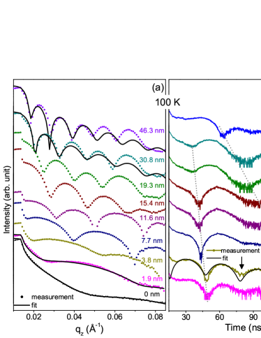
Similar to the procedures followed for in-situ NRS measurements at 300 K, the growth of FeN films was also studied by cooling the substrate holder by a continuous flow of LN2. Prior to cooling the sample holder, the whole system was baked to achieve UHV conditions which is an essential requirement to avoid condensation of moisture on the substrate surface at LN2 temperatures. The estimated temperature at the sample surface was about 100 K and films of different thicknesses were deposited at this temperature. Figure 5(a) and (b) shows XRR and NRS patterns for FeN films of different thicknesses. Here again total thickness oscillations can be seen in the XRR pattern (fig. 5(a)) yielding the thickness of films. The deposition rate estimated from the known deposition time was about 7.7 nm/min which was more than twice than that of samples deposited at 300 K (3.4 nm/min). Such enhancement in deposition rates is not unexpected at LN2 temperatures as evidenced recently during the growth of nickel oxide thin films 2018_JVST_NiO_LT . From the fitting of XRR patterns, we found that the density of films deposited at 100 K was similar to those at 300 K. More interesting behavior can be seen in the NRS patterns shown in fig. 5(b). Here broad oscillation correspond to dynamical beats(DBs) PRB_DB_1 ; PRB_DB_2 originating due to the total thickness of sample (marked by dashed lines) can be seen. With an increase in thickness DBs shift to lower time in agreement with the behavior that can also be seen in samples deposited at 300 K (fig. 3(b)).
On the other hand, an additional beating pattern can be seen in ultrathin films ( 7.7 nm) and more prominently for the 3.8 nm film. It is known that in the presence of hyperfine interactions due to electric quadrupole or magnetic dipole, nuclear levels show quadrupole or Zeeman splitting. During the nuclei de-excitation process interference amplitudes give rise to oscillations in the scattered intensity with time. These oscillations are known as quantum beats (QBs) PRL_QB_1 . The periods and amplitudes of QBs reveal the information about the magnetic structure present in the sample. The absence of QBs in our NRS pattern is a characteristic of a non-magnetic sample. These QBs are quite clearly visible in the 3.8 nm sample, and their presence, though weak, can also be seen in the 1.9 and 7.7 nm films. The positions of QBs is marked by an arrow in fig 5(b). The presence of QBs indicates that the sample possess a magnetic structure. In order to find the nature of magnetism, the NRS spectra was fitted using REFTIM software REFTIM2008 . Assuming a hyperfine field of about 15 T, the the period of QBs matches well with our experimental data. This value is smaller than the hyperfine filed of 30 T expected for the AFM RS-type FeN 2013_HI_FeN_PLD ; 2015_RSC_ADV_mag_order . Nevertheless, the presence of magnetic state in our ultrathin FeN films confirm that RS-type FeN indeed possess a magnetic ground state. Since samples in our study have been deposited at about 100 K, it can be anticipated that crystalline ordering may not get established due to lack of adatom mobility and therefore in this situation structural disorders may lead to a smaller hyperfine filed evidenced in the 3.8 nm film. Ideally, by depositing the film at a higher substrate temperature around 450 K and then cooling it down to low temperature, precise determination of the magnetic structure can be made.
A close correlation can be drawn between the N -edge XANES and the 100 K NRS pattern of ultrathin ( 5 nm) FeN thin films. At such a low thickness their value is large (4.4 eV), the ratio of features is also large and they are antiferromagnetic. The octahedral coordination between Fe and N atoms confirm the RS-type structure and the presence of AFM ground state further confirms it. From the observed growth behavior, it appears that initially FeN films grow in the RS-type structure, subsequently due to an in plane tensile stress, films are forced to adopt the ZB-type structure. Such transformation in the structure was also evidenced by J. Pak et al. JPak_2010 during the in-situ growth and study of epitaxial FeN films. It was found that the LP was 4.52 Å in the beginning and when the thickness increases to about 60 nm it reduces to 4.32 Å. It seems that the critical thickness at which such transition takes place will depend upon the growth temperature, in our case films are grown at 300 K and the RS to ZB-type structural transition is taking place around 5 nm but when films were grown at high temperature (e.g. 483 K by J. Pak. et al.), such transition was taking place at a much larger thickness. It is anticipated that by growing FeN films at high substrate temperature and then by studying the magnetic properties of ultrathin films at low temperature more precise estimation of magnetic ground state of FeN can be made.
IV Conclusions
In this work structure and magnetic properties of ultrathin FeN films were studied during in-situ growth using N -edge XANES at 300 K and NRS measurements at 300 and 100 K. N -edge XANES measurements clearly reveal that coordination between Fe and N atoms changes from octahedral (RS-type FeN) to tetrahedral (ZB-type FeN) when thickness increases beyond 5 nm. Low temperature NRS measurements also depict such behavior as RS-type FeN films show an antiferromagnetic character. When the thickness of films increases beyond 5 nm films become non-magnetic as expected in for ZB-type FeN. The remarkable sensitivity of both XANES and NRS for ultrathin layers can further be utilized by growing FeN films at high temperatures and then studying the structural and magnetic properties at low temperatures.
Acknowledgements.
We would like to thank to the Department of Science and Technology, India for the financial support and Jawaharlal Nehru Centre for Advanced Scientific Research (JNCASR) for managing the project. We acknowledge technical help received from L. Behera, A. Gome and R. Sah. We are thankful to V. Ganesan and A. K. Sinha for support and encouragements.References
- (1) S. Bhattacharyya, The Journal of Physical Chemistry C 119, 1601 (2015).
- (2) M. Takahashi, H. Shoji, J. Magnetism and Magnetic Materials 208, 145 (2000).
- (3) Y. Jiang, M.A. Mehedi, E. Fu, Y. Wang, L.F. Allard, J.P. Wang, Scientific Reports 6, 25436 (2016).
- (4) S. Kokado, N. Fujima, K. Harigaya, H. Shimizu, A. Sakuma, Phys. Rev. B 73, 172410 (2006).
- (5) A. Houari, S.F. Matar, M.A. Belkhir, Journal of Magnetism and Magnetic Materials 322, 658 (2010).
- (6) K. Ito, G.H. Lee, K. Harada, M. Suzuno, T. Suemasu, Y. Takeda, Y. Saitoh, M. Ye, A. Kimura, H. Akinaga, Applied Physics Letters 98, 102507 (2011).
- (7) E.L.P.y. Blancá, J. Desimoni, N.E. Christensen, H. Emmerich, S. Cottenier, physica status solidi (b) 246, 909 (2009).
- (8) H. Li, X. Li, D. Kim, G. Zhao, D. Zhang, Z. Diao, T. Chen, J.P. Wang, Applied Physics Letters 112, 162407 (2018).
- (9) W. Yin, D. Zhang, P. Zhang, X. Wang, W. Wang, X. Lei, Z. Shi, H. Yang, Journal of Alloys and Compounds 688, 828 (2016).
- (10) H. Huang, S. Gao, A.M. Wu, K. Cheng, X.N. Li, X.X. Gao, J.J. Zhao, X.L. Dong, G.Z. Cao, Nano Energy 31, 74 (2017).
- (11) Nuclear Instruments and Methods in Physics Research Section B: Beam Interactions with Materials and Atoms 168, 422 (2000).
- (12) D. Laniel, A. Dewaele, G. Garbarino, Inorganic Chemistry 57, 6245 (2018).
- (13) Y.N. Xu, P. Rulis, W.Y. Ching, J. Appl. Phys. 91, 7352 (2002).
- (14) W.Y. Ching, Y.N. Xu, P. Rulis, Applied Physics Letters 80, 2904 (2002).
- (15) M. Wessel, R. Dronskowski, Chemistry A European Journal 17, 2598.
- (16) M. Bykov, E. Bykova, G. Aprilis, K. Glazyrin, E. Koemets, I. Chuvashova, I. Kupenko, C. McCammon, M. Mezouar, V. Prakapenka, H.P. Liermann, F. Tasnádi, A.V. Ponomareva, I.A. Abrikosov, N. Dubrovinskaia, L. Dubrovinsky, Nature Communications 9, 2756 (2018).
- (17) L. Wu, R. Tian, B. Wan, H. Liu, N. Gong, P. Chen, T. Shen, Y. Yao, H. Gou, F. Gao, Chemistry of Materials 30, 8476 (2018).
- (18) K.H. Jack, Proceedings of the Royal Society of London. Series A. Mathematical and Physical Sciences 208, 200 (1951).
- (19) A. Oueldennaoua, E. Bauer-Grosse, M. Foos, C. Frantz, Scripta Metall. 19, 1503 (1985).
- (20) H. Nakagawa, S. Nasu, H. Fujii, M. Takahashi, F. Kanamaru, Hyperfine Interact. 69, 455 (1991).
- (21) K. Suzuki, H. Morita, T. Kaneko, H. Yoshida, H. Fujimori, J. Alloys Compds. 201, 11 (1993).
- (22) T. Hinomura, S. Nasu, Physica B: Condensed Matter 237-238, 557 (1997).
- (23) P. Schaaf, C. Illgner, M. Niederdrenk, K.P. Lieb, Hyp. Int. 95, 199 (1995).
- (24) M. Niederdrenk, P. Schaaf, K.P. Lieb, O. Schulte, J. Alloys and Compd. 237, 81 (1996).
- (25) L. Rissanen, M. Neubauer, K.P. Lieb, P. Schaaf, J. Alloys and Compds. 274, 74 (1998).
- (26) P. Schaaf, Prog. Mater. Sci. 47, 1 (2002).
- (27) M. Gupta, A. Gupta, S. Chaudhari, D. M. Phase, V. Ganesan, M.R. Rao, T. Shripathi, B. Dasannacharya, Vacuum 60, 395 (2001).
- (28) X. Wang, W. Zheng, H. Tian, S. Yu, W. Xu, S. Meng, X. He, J. Han, C. Sun, B. Tay, Appl. Sur. Sci. 220, 30 (2003).
- (29) D. Peng, T. Hihara, K. Sumiyama, Journal of Alloys and Compounds 377, 207 (2004).
- (30) R. Gupta, M. Gupta, Phys. Rev. B 72, 024202 (2005).
- (31) V. Demange, T.H. Loi, P. Weisbecker, E. Bauer-Grosse, Thin Solid Films 494, 184 (2006).
- (32) I. Jouanny, P. Weisbecker, V. Demange, M. Grafouté, O. Peña, E. Bauer-Grosse, Thin Solid Films 518(8), 1883 (2010).
- (33) M. Gupta, A. Tayal, A. Gupta, R. Gupta, J. Stahn, M. Horisberger, A. Wildes, J. Appl. Phys. 110, 123518 (2011).
- (34) M. Gupta, A. Tayal, A. Gupta, V. Reddy, M. Horisberger, J. Stahn, J. Alloys and Compounds 509, 8283 (2011).
- (35) A. Tayal, M. Gupta, A. Gupta, P. Rajput, J. Stahn, Phys. Rev. B 92, 054109 (2015).
- (36) A. Tayal, M. Gupta, N. Pandey, A. Gupta, M. Horisberger, J. Stahn, Journal of Alloys and Compounds 650, 647 (2015).
- (37) Materials Today: Proceedings 4, 6173 (2017).
- (38) Q. Lu, M. Xie, G. Han, B. Zheng, Y. Song, J. Qiang, X. Wang, Z. Wu, P. Yan, W. Liu, Journal of Magnetism and Magnetic Materials 474, 76 (2019).
- (39) M. Gupta, A. Gupta, P. Bhattacharya, P. Misra, L. Kukreja, J. Alloys and Compounds 326, 265 (2001).
- (40) F. Sun, J. Liu, Y. Yang, H. Yu, Materials Science and Engineering: B 122, 29 (2005).
- (41) R. Usui, Y. Yamada, Y. Kobayashi, Hyperfine Interactions 205, 13 (2012).
- (42) Y. Yamada, R. Usui, Y. Kobayashi, Hyperfine Interactions 219, 13 (2013).
- (43) A. Tayal, M. Gupta, A. Gupta, V. Ganesan, L. Behera, S. Singh, S. Basu, Surface and Coatings Technology 275, 264 (2015).
- (44) C. Navío, J. Alvarez, M.J. Capitan, F. Yndurain, R. Miranda, Phys. Rev. B 78, 155417 (2008).
- (45) D.M. Borsa, D.O. Boerma, Hyperfine Interactions 151, 31 (2003).
- (46) E. Andrzejewska, R. Gonzalez-Arrabal, D. Borsa, D. Boerma, Nuclear Instruments and Methods in Physics Research Section B: Beam Interactions with Materials and Atoms 249, 838 (2006).
- (47) J. Pak, W. Lin, K. Wang, A. Chinchore, M. Shi, D.C. Ingram, A.R. Smith, K. Sun, J.M. Lucy, A.J. Hauser, F.Y. Yang, Journal of Vacuum Science & Technology A 28, 536 (2010).
- (48) M. Naito, K. Uehara, R. Takeda, Y. Taniyasu, H. Yamamoto, Journal of Crystal Growth 415, 36 (2015)
- (49) K. Niwa, T. Terabe, D. Kato, S. Takayama, M. Kato, K. Soda, M. Hasegawa, Inorganic Chemistry 56, 6410 (2017).
- (50) D. Laniel, A. Dewaele, S. Anzellini, N. Guignot, Journal of Alloys and Compounds 733, 53 (2018).
- (51) W.P. Clark, S. Steinberg, R. Dronskowski, C. McCammon, I. Kupenko, M. Bykov, L. Dubrovinsky, L.G. Akselrud, U. Schwarz, R. Niewa, Angewandte Chemie International Edition 56, 7302 (2017).
- (52) M. Zheng, X. Chen, R. Cheng, N. Li, J. Sun, X. Wang, T. Zhang, Catalysis Communications 7, 187 (2006).
- (53) Z. Yang, S. Guo, X. Pan, J. Wang, X. Bao, Energy Environ. Sci. 4, 4500 (2011).
- (54) C. Navío, J. Alvarez, M.J. Capitan, J. Camarero, R. Miranda, Appl. Phys. Lett. 94, 263112 (2009).
- (55) C. Navío, M.J. Capitán, J. Álvarez, R. Miranda, F. Yndurain, New J. Phys. 12, 073004 (2010)
- (56) S. Li, X. Cui, Z.F. Liu, T.L. Song, Journal of Alloys and Compounds 771, 322 (2019).
- (57) Journal of Physics and Chemistry of Solids 100, 148 (2017).
- (58) Z. Zhao, K. Bao, D. Duan, F. Tian, B. Liu, T. Cui, RSC Adv. 5, 31270 (2015).
- (59) Journal of Alloys and Compounds 603, 172 (2014).
- (60) Journal of Alloys and Compounds 522, 106 (2012).
- (61) A. Houari, S.F. Matar, M.A. Belkhir, M. Nakhl, Phys. Rev. B 75, 064420 (2007).
- (62) J.G. Chen, Surface Science Reports 30, 1 (1997).
- (63) R. Rüffer, A.I. Chumakov, Hyperfine Interactions 97, 589 (1996).
- (64) D.M. Phase, M. Gupta, S. Potdar, L. Behera, R. Sah, A. Gupta, AIP Conference Proceedings 1591, 685 (2014).
- (65) Dynamics beamline p01 web site. http://photon-science.desy.de/facilities/petra_iii/beamlines/p01_dynamics/index_eng.html
- (66) Journal of Alloys and Compounds 508, 233 (2010).
- (67) M. Tallarida, C. Das, D. Schmeisser, Beilstein J. Nanotechnol. 5, 77 (2014).
- (68) R. Gupta, M. Gupta, D.M. Phase, AIP Conference Proceedings 1832, 080081 (2017).
- (69) P. Vishwakarma, M. Gupta, D.M. Phase, A. Gupts, Journal of Physics: Condensed Matter 31, 105001 (2019).
- (70) H. Wille, H. Franz, R. Röhlsberger, W. Caliebe, F. Dill, in Journal of Physics: Conference Series 217 012008 (2010).
- (71) Journal of Electron Spectroscopy and Related Phenomena 189, 187 (2013).
- (72) G.V. Smirnov, Hyperfine Interactions 97(1), 551 (1996).
- (73) Comptes Rendus Physique 9(5), 595 (2008).
- (74) R. Röhlsberger, Nuclear Condensed Matter Physics with Synchrotron Radiation, vol. 208 Springer-Verlag (2004).
- (75) Journal of Crystal Growth 415, 36 (2015).
- (76) Journal of Electron Spectroscopy and Related Phenomena 62, 197 (1993).
- (77) Solid State Communications 130(3), 209 (2004).
- (78) Y. Tripathi, R. Gupta, Seema, M. Gupta, D. Phase, P. Rajput, Thin Solid Films 670, 113 (2019).
- (79) Y. Abe, S. Yamauchi, M. Kawamura, K.H. Kim, T. Kiba, Journal of Vacuum Science & Technology A 36, 02C102 (2018).
- (80) U. van Bürck, W. Potzel, P. Schindelmann, Y.V. Shvyd ko, E. Gerdau, O. Leupold, H. Rüter, Physical Review A 61, 013803 (1999).
- (81) Y.V. Shvyd ko, U. Van Bürck, W. Potzel, P. Schindelmann, E. Gerdau, O. Leupold, J. Metge, H. Rüter, G. Smirnov, Physical Review B 57(6), 3552 (1998).
- (82) E. Gerdau, R. Rüffer, R. Hollatz, J. Hannon, Physical review letters 57(9), 1141 (1986).
- (83) M.A. Andreeva, Hyperfine Interactions 185(1), 17 (2008).