Topology optimization of freeform large-area metasurfaces
Abstract
We demonstrate optimization of optical metasurfaces over – degrees of freedom in two and three dimensions, 100–1000+ wavelengths () in diameter, with 100+ parameters per . In particular, we show how topology optimization, with one degree of freedom per high-resolution “pixel,” can be extended to large areas with the help of a locally periodic approximation that was previously only used for a few parameters per . In this way, we can computationally discover completely unexpected metasurface designs for challenging multi-frequency, multi-angle problems, including designs for fully coupled multi-layer structures with arbitrary per-layer patterns. Unlike typical metasurface designs based on subwavelength unit cells, our approach can discover both sub- and supra-wavelength patterns and can obtain both the near and far fields.
1 Introduction
We present a method for large-area ( wavelengths ) topology optimization (TO) [1, 2, 3] of optical “metasurfaces” [4, 5] with millions of degrees of freedom (DoF) determined automatically. Whereas previous metasurface design methods used only a few parameters per subwavelength unit cell [5, 6, 7, 8, 9, 10, 11, 12, 13], TO allows us to consider thousands of parameters per unit cell, with much larger () unit cells in which both sub-wavelength and supra-wavelength features are discovered by making every “pixel” a DoF. Whereas previous TO methods in optics were restricted to computational domains amenable to brute-force simulation [14, 15], we exploit a locally periodic approximation [6, 7, 8, 9, 10, 11, 12, 16] to combine many smaller simulations into a single optimization problem for a huge surface (Sec. 2). We validate example designs for high numerical-aperture (NA) multi-frequency/multi-angle lenses in 2d against full-wave simulations of the entire domain (Sec. 3.1 and 3.2). We also present example 3d designs for monochromatic high-NA lenses with DoF (Sec. 3.3), enabled by an efficient massively parallel implementation combining thousands of RCWA (rigorous coupled-wave analysis) unit-cell solutions [17, 18] and fast adjoint-method [1, 3] gradient computations. Because our method employs the full scattered field for each surface unit, as opposed to a single phase or amplitude in previous works [5, 6, 7, 8, 9, 10, 11, 12], we could also apply our method to near-field or guided-wave optimization [19] (Sec. 4).
Metasurfaces offer ultra-compact flat-optics alternatives for traditional bulky systems used in lensing, beam-shaping, holography and beyond [20]. The power and versatility of a metasurface resides in aperiodically patterned nanophotonic features covering hundreds or thousands of wavelengths in diameter. The term “meta" often refers to extremely subwavelength features that may be modeled by effective surface impedances [21], but in this work we consider both sub- and supra-wavelength features and do not employ any effective-medium approximation. Understandably, a meta-device poses a more challenging design problem than a traditional optical system since it requires an understanding and control of electromagnetic interactions within a vast number of nanostructures. Typically, such interactions are handled by a locally periodic approximation (LPA) in which the metasurface is divided into computationally tractable independent unit cells with periodic boundary conditions [5, 6, 7, 8, 9, 10, 11, 12]. One extreme limit of LPA is scalar diffraction theory [22], in which the surface is treated as locally uniform; this is often used to design diffractive surfaces [23] but is unlikely to accurately model subwavelength patterns. Meanwhile, the geometric library which provides the “meta-elements" is made up of primitive shapes such as subwavelength cylindrical or rectangular pillars which can be rapidly modeled (under LPA) by an electromagnetic solver such as RCWA [5, 6, 7, 8, 9, 10, 11, 12]. However, it may become increasingly difficult and ultimately infeasible to leverage only simple primitive geometries for more complex problems such as broadband achromatic focusing [24, 25, 26] or controlled angular dispersion [27] which impose stringent demands on the local phase shifts provided by the meta-elements.
Topology optimization (TO) is a large-scale computational technique that can handle an extensive design space, considering the dielectric permittivity at every spatial point as a DoF [1, 2, 3]. In contrast to the heuristic search routines regularly employed by the photonic community such as genetic algorithms [28] or particle swarm methods [29], TO employs gradient-based optimization techniques to explore hundreds to billions of continuous DoFs. Such a capability is made possible by a rapid computation of gradients (with respect to all the DoFs) via adjoint methods [30], which, in the context of electromagnetic inverse design, involve just one additional solution of Maxwell’s equations [3]. In fact, such techniques have been gaining traction lately in the field of photonic integrated circuits, especially for the design of compact modal multiplexers and converters [31]. Only recently, TO-based inverse design methods have been extended to metasurfaces, particularly in the context of freeform meta-gratings [14] and metalenses with angular phase control [15]. While such applications reveal TO as a very promising tool for realizing increasingly sophisticated meta-devices, they have been limited to small computational domains . In this paper, we present a combination of TO and LPA to efficiently design large-area metasurfaces with enhanced functionalities.
2 Formulation
Because we employ a general optimization framework, we have great flexibility in what function of the electromagnetic fields to optimize (our “objective” function ) [16]. For many light-focusing problems, it is convenient to simply maximize the electric-field intensity at a focal point [16]:
| (1) | ||||
Here, the set of DoFs is related to the position-dependent dielectric profile via , where denotes the relative permittivity of the structural (background) dielectric material. Whereas is a continuous DoF allowed to have intermediate values between 0 and 1, we employ Heaviside projection filters [1] to ensure that the final optimal design is binary, i.e., . In this work, we consider only the binary filter to theoretically illustrate our design method. More generally, a variety of additional geometric filters and constraints can be straightforwardly incorporated into the formulation, including regularization filters and curvature constraints [1, 32, 33] to impose design robustness and minimum feature sizes conducive to fabrication. The objective function represents the far-field intensity obtained by convolving the free-space Green’s function with the near-field at some reference plane over the entire metasurface. (To be precise, the free-space Green’s function is convolved with equivalent surface currents which are given by the tangential field components [34].) Here, is the steady-state solution to the frequency-domain Maxwell’s equation:
| (2) |
in response to the incident current at a frequency where we set the magnetic permeability for typical optical materials. To efficiently model a large device area, we use the locally periodic approximation [16], in which the metasurface is broken up into multiple smaller cells, each of which is independently simulated with periodic boundary conditions (Fig. 1). The total near-field is, therefore, approximated by the set of disjoint intra-cell electric fields which must be engineered such that they all constructively add up at the focal point. The optimization typically involves thousands of DoFs which must be efficiently handled by a numerical algorithm. Within the scope of TO, this requires efficient calculations of the derivatives at every pixel point in the device region, which we obtain by an adjoint method [3, 30]:
| (3) | ||||
| (4) |
where the adjoint field is evaluated by solving an additional Maxwell’s equation:
| (5) |
We emphasize that our framework is entirely different from the common approach where an ideal phase profile to be realized is approximately fitted with zeroth-order phase shifts allowed by primitive scattering elements, each residing within a sub-wavelength unit cell [5, 6, 7, 8, 9, 10, 11, 12]. In contrast, our approach greatly broadens the structural design space by considering non-intuitive shapes and forms as well as supra-wavelength unit cells within which the amplitude and phase of the electric field may vary considerably and must be fully taken into account during optimization.
2.1 Numerical Implementation
To ensure a speedy computation, we numerically implement the optimization problem (1) in C. Each of the cells is either solved by a C implementation of the finite-difference frequency-domain method (FDFD) [35] or the rigorous coupled-wave analysis (RCWA) [18]. To model a large surface area rapidly, all the cells are independently simulated in an “embarrassingly parallel” fashion using the message-passing interface (MPI) library [36, 37]. The simulated results are then consolidated to compute the global objective and gradients. The structural update during optimization is provided by a standard gradient-based nonlinear-optimization algorithm [38, 39] with a free-software implementation [40]. We note that the discretization error in the gradients arising from the discrepancy between the formal adjoint method and the numerical Maxwell’s solver (such as RCWA) is practically negligible ().
3 Applications
The major advantage of a large-scale computational approach consists in its flexibility for handling multi-objective problems, such as those prescribing the behavior of a single metasurface for a set of frequencies and incident current conditions . In such cases, the optimization problem can be easily extended by the maximin formulation:
| (6) |
which can be recast into an equivalent differentiable form [41]:
| (7) | ||||
| (8) |
3.1 Metalens Concentrator
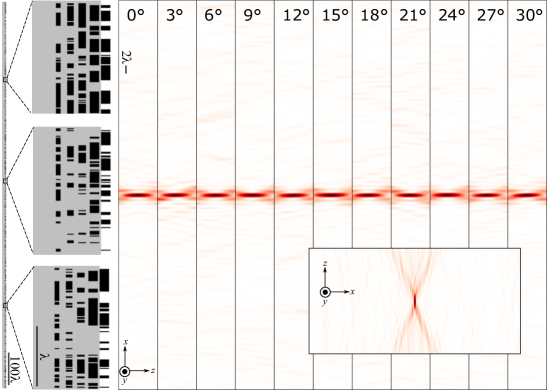
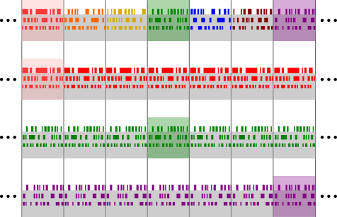
To demonstrate the efficacy of our design technique, we optimize a multi-layered 2D metalens (Fig. 2) that can concentrate incoming light at 11 incident angles to the same focus. The lens consists of five layers of TiO2 (refractive index ), four of which are buried in silica (). The diameter of the lens is , where is the operational wavelength, and the focal length is , corresponding to a rather high NA of 0.51. For simplicity, we consider the electric field to be polarized along the axis. During the optimization, the entire lens is broken up into 240 cells, each of which is long, for DoFs in total, while the entire computation is parallelized over 1200 CPUs. While we perform the optimization with the locally periodic approximation, we validate the optimized result with rigorous full-wave FDTD simulations [42] (Fig. 2) in which we compute the actual electric fields over the entire metasurface without any uncontrolled approximation. The lens is shown to exhibit diffraction-limited focusing at all the optimized angles with the full-width-at-maximum (FWHM) of while the average transmission efficiency is found to be . The average efficiency of seems to violate Lorentz reciprocity and, in particular, the concentration bound predicted by [43]. However, there is no such violation because, although the output field profiles have the same prominent peak at the optical axis, they are never entirely alike for any two input angles due to the weak but distinct diffracting patterns away from the axis.
3.2 Multi-wavelength Focusing
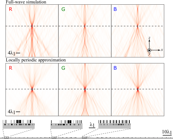
Another example we consider is a partially achromatic 2D metalens (Fig. 3) with discrete chromatic aberration corrections at three wavelengths with and . In particular, one may choose , and , corresponding to red, green and blue (RGB) wavelengths. The lens consists of two layers of TiO2 (), one of which is buried in silica (). The diameter of the lens is and the focal length is , corresponding to . During the optimization, the entire lens is broken up into 40 cells, each of which is long, for DoFs in total, while the entire computation is parallelized over just 20 CPUs. At the desired frequencies, the lens is shown to focus a normally incident -polarized beam at or near the diffraction limit with the FWHMs of and respectively and with an average transmission efficiency of . Recently, broadband achromatic metalenses have been gaining widespread attention for full color imaging; although the state-of-the-art designs continuously cover the full visible spectrum, they are mostly limited to smaller lens diameters and/or low NA [24, 25, 26]. Our results suggest that multi-layer designs enabled by TO could alleviate many of these limitations by allowing more complex geometries to be explored.
Generally, a high-NA multi-wavelength design is a challenge for LPA because the design rapidly varies across the surface, resulting in the scattering “noise” visible in a full-wave simulation of the entire structure but not captured by the conjoined LPA solution (Fig. 3), in contrast to the multi-angle case in Fig. 2. One consequence is that the focusing efficiencies at the three wavelengths (defined as the integrated field intensity around the focal spot divided by the total intensity over the image plane [44]) are found to be and while LPA predicts and respectively. Note that our objective function (1) merely maximizes the intensity at the focal spot but does not necessarily suppress stray diffractions elsewhere which become apparent even in LPA predictions (Fig. 3). If desired, the optimal design can be further refined by improving the LPA wavefront by minimizing a phase error [15] or wavefront error objective [16]. At the same time, deviations from LPA may be mitigated by considering larger metasurfaces where LPA is more appropriate, by including higher-order corrections to LPA [19], or by incorporating optimization constraints designed to enforce the validity of LPA. For example, the optimization process may be augmented with constraints restricting the structural variations between neighboring cells or specifying a bound on the physical residual:
| (9) |
where the double curl operator is applied over the whole surface without LPA. Note that evaluating the residual requires just a single matrix-vector multiplication, albeit involving a very large and sparse matrix, and can be made relatively cheap and fast when parallelized over several cores.
3.3 Three-dimensional Examples
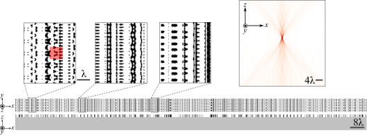
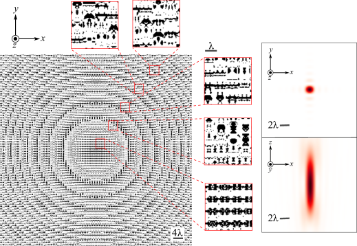
Next, we turn to proof-of-concept 3D examples. First, we consider a collection of 3D cells, each of which has an area . The cells are repeated along but are allowed to differ from each other along . Fig. 4 shows the corresponding “cylindrical” lens (NA=0.71) comprising such cells which focuses a normally-incident -polarized beam to a focal line running parallel to the -axis. The lens, though periodic along , shows complex geometric variations along both and within each cell. A rigorous FDTD simulation of the whole lens shows the focusing behavior with a transmission efficiency of 75%. Although the design of a monochromatic lens, no matter the geometric complexity, is only useful to illustrate the method, we note that our framework enables a relatively cheap and fairly quick computation using as few as 25 CPUs over a span of a few minutes while considering the entire structure with as many as 200 cells and DoFs in total.
Lastly, we consider the full 3D lens (Fig. 5) with cells varying along both and . The lens has 6400 cells, corresponding to NA=0.37, with DoFs in total. Again, our framework enables a cheap and speedy design of the entire lens, utilizing 40 CPUs and lasting only a few minutes. A major computational hurdle actually arises after the optimization: given the enormous size, the lens cannot be readily simulated via FDTD using a few CPUs. Instead, we provide an approximate far-field profile computed from the LPA combination of the unit-cell simulations, which has been shown to give excellent accuracy for monochromatic designs [13] and good accuracy even for the complex multi-frequency designs in Sec. 3.2.
These preliminary results suggest promising ways to scale up the 3D metasurface design. In particular, the computational workload can be reduced by orders of magnitude via rotational symmetry, specifically, by considering just a single row of cells and rotating it to fully cover the entire surface. Such an approach is, in fact, a more common practice in metalens design [5, 6, 7, 8, 9, 10, 11, 12, 13] rather than considering all the cells as we did here. Also, polarization insensitivity could be ensured by further imposing appropriate symmetries, such as within each cell. Combined with such symmetry-related reductions, an access to several hundreds or low thousands of CPUs (readily available on institutional supercomputers or commercial cloud computing services) amply allow for the design of high-NA wide-area metalenses with greatly enhanced functionalities including broadband achromaticity and large-angle aberration corrections.
4 Conclusion and Outlook
We have provided an efficient computational framework for the inverse design of large-area freeform metasurfaces. We have also presented various examples including multi-angle and multi-wavelength metalens designs that demonstrate the versatility and power of our method. We expect that a large-scale optimization technique like ours may become indispensable for tackling challenging problems which inherently call for a large design space with multiple layers. In particular, our method may greatly benefit the design of a polarization-insensitive large-area high-NA single-piece metalens with chromatic and achromatic aberration corrections over the entire visible spectrum and over a large field of view. On the other hand, our framework need not be limited to metalens design. In fact, the particular objective we presented above might be more naturally suited for three-dimensional sculpting of the far-field intensity (or thin-film holography). Another intriguing application particularly suitable for the RCWA-based optimization framework is to inverse-design the far field between two meta-devices separated by thick (many-wavelengths) spacing layers. Ultimately, one would like to address the most challenging problem of electromagnetic design: to intimately manipulate the near-field physics of large aperiodic structures in which ultra-rich modal interactions involving both extended and localized resonances may offer a superb playground for exploring novel phenomena and devising next-generation technologies such as solid-state Lidar systems [45], strongly enhanced light-matter interactions and nonlinear processes [46, 47, 48, 49, 50], near-field radiative heat transfer [51], and opto-nanomechanical engineering [52, 53]. While LPA offers asymptotic advantages in the limit of “adiabatic” nearly periodic surfaces, our optimization framework also provides a promising pathway for handling a wider variety of large aperiodic systems by incorporating additional constraints (Sec. 3.2) or by augmenting LPA with domain decomposition concepts [54] including using the conjoined LPA solution as a preconditioner, using other boundary conditions (e.g. mirror boundaries), and using overlapping domains [55, 56].
References
- [1] Jakob Søndergaard Jensen and Ole Sigmund. Topology optimization for nano-photonics. Laser & Photonics Reviews, 5(2):308–321, 2011.
- [2] Christopher M Lalau-Keraly, Samarth Bhargava, Owen D Miller, and Eli Yablonovitch. Adjoint shape optimization applied to electromagnetic design. Optics Express, 21(18):21693–21701, 2013.
- [3] Sean Molesky, Zin Lin, Alexander Y Piggott, Weiliang Jin, Jelena Vucković, and Alejandro W Rodriguez. Inverse design in nanophotonics. Nature Photonics, 12(11):659, 2018.
- [4] Nanfang Yu, Patrice Genevet, Mikhail A Kats, Francesco Aieta, Jean-Philippe Tetienne, Federico Capasso, and Zeno Gaburro. Light propagation with phase discontinuities: generalized laws of reflection and refraction. Science, page 1210713, 2011.
- [5] Nanfang Yu and Federico Capasso. Flat optics with designer metasurfaces. Nature materials, 13(2):139, 2014.
- [6] Francesco Aieta, Patrice Genevet, Mikhail A Kats, Nanfang Yu, Romain Blanchard, Zeno Gaburro, and Federico Capasso. Aberration-free ultrathin flat lenses and axicons at telecom wavelengths based on plasmonic metasurfaces. Nano Letters, 12(9):4932–4936, 2012.
- [7] Francesco Aieta, Mikhail A Kats, Patrice Genevet, and Federico Capasso. Multiwavelength achromatic metasurfaces by dispersive phase compensation. Science, 347(6228):1342–1345, 2015.
- [8] Mohammadreza Khorasaninejad, Francesco Aieta, Pritpal Kanhaiya, Mikhail A Kats, Patrice Genevet, David Rousso, and Federico Capasso. Achromatic metasurface lens at telecommunication wavelengths. Nano Letters, 15(8):5358–5362, 2015.
- [9] Mohammadreza Khorasaninejad, Wei Ting Chen, Alexander Y Zhu, Jaewon Oh, Robert C Devlin, Charles Roques-Carmes, Ishan Mishra, and Federico Capasso. Visible wavelength planar metalenses based on titanium dioxide. IEEE Journal of Selected Topics in Quantum Electronics, 23(3):43–58, 2017.
- [10] Mohammadreza Khorasaninejad, Zhujun Shi, Alexander Y Zhu, Wei-Ting Chen, Vyshakh Sanjeev, Aun Zaidi, and Federico Capasso. Achromatic metalens over 60 nm bandwidth in the visible and metalens with reverse chromatic dispersion. Nano Letters, 17(3):1819–1824, 2017.
- [11] Ehsan Arbabi, Amir Arbabi, Seyedeh Mahsa Kamali, Yu Horie, and Andrei Faraon. Controlling the sign of chromatic dispersion in diffractive optics with dielectric metasurfaces. Optica, 4(6):625–632, 2017.
- [12] Vin-Cent Su, Cheng Hung Chu, Greg Sun, and Din Ping Tsai. Advances in optical metasurfaces: fabrication and applications. Optics Express, 26(10):13148–13182, 2018.
- [13] Mohammadreza Khorasaninejad, Wei Ting Chen, Robert C Devlin, Jaewon Oh, Alexander Y Zhu, and Federico Capasso. Metalenses at visible wavelengths: Diffraction-limited focusing and subwavelength resolution imaging. Science, 352(6290):1190–1194, 2016.
- [14] David Sell, Jianji Yang, Sage Doshay, Rui Yang, and Jonathan A Fan. Large-angle, multifunctional metagratings based on freeform multimode geometries. Nano Letters, 17(6):3752–3757, 2017.
- [15] Zin Lin, Benedikt Groever, Federico Capasso, Alejandro W Rodriguez, and Marko Lončar. Topology-optimized multilayered metaoptics. Physical Review Applied, 9(4):044030, 2018.
- [16] Raphaël Pestourie, Carlos Pérez-Arancibia, Zin Lin, Wonseok Shin, Federico Capasso, and Steven G Johnson. Inverse design of large-area metasurfaces. Optics Express, 26(26):33732–33747, 2018.
- [17] MG Moharam and TK Gaylord. Rigorous coupled-wave analysis of planar-grating diffraction. JOSA, 71(7):811–818, 1981.
- [18] Victor Liu and Shanhui Fan. S4 : A free electromagnetic solver for layered periodic structures. Computer Physics Communications, 183(10):2233 – 2244, 2012.
- [19] Carlos Pérez-Arancibia, Raphaël Pestourie, and Steven G. Johnson. Sideways adiabaticity: beyond ray optics for slowly varying metasurfaces. Opt. Express, 26(23):30202–30230, Nov 2018.
- [20] Federico Capasso. The future and promise of flat optics: a personal perspective. Nanophotonics, 7(6):953–957, 2018.
- [21] Carl Pfeiffer and Anthony Grbic. Metamaterial Huygens’ surfaces: tailoring wave fronts with reflectionless sheets. Physical Review Letters, 110(19):197401, 2013.
- [22] Max Born and Emil Wolf. Principles of Optics: Electromagnetic Theory of Propagation, Interference and Diffraction of Light. Elsevier, 2013.
- [23] Ganghun Kim, José A Domínguez-Caballero, and Rajesh Menon. Design and analysis of multi-wavelength diffractive optics. Optics Express, 20(3):2814–2823, 2012.
- [24] Wei Ting Chen, Alexander Y Zhu, Vyshakh Sanjeev, Mohammadreza Khorasaninejad, Zhujun Shi, Eric Lee, and Federico Capasso. A broadband achromatic metalens for focusing and imaging in the visible. Nature nanotechnology, 13(3):220, 2018.
- [25] Shuming Wang, Pin Chieh Wu, Vin-Cent Su, Yi-Chieh Lai, Mu-Ku Chen, Hsin Yu Kuo, Bo Han Chen, Yu Han Chen, Tzu-Ting Huang, Jung-Hsi Wang, et al. A broadband achromatic metalens in the visible. Nature nanotechnology, 13(3):227, 2018.
- [26] Sajan Shrestha, Adam C Overvig, Ming Lu, Aaron Stein, and Nanfang Yu. Broadband achromatic dielectric metalenses. Light: Science & Applications, 7(1):85, 2018.
- [27] Seyedeh Mahsa Kamali, Ehsan Arbabi, Amir Arbabi, Yu Horie, MohammadSadegh Faraji-Dana, and Andrei Faraon. Angle-multiplexed metasurfaces: Encoding independent wavefronts in a single metasurface under different illumination angles. Physical Review X, 7(4):041056, 2017.
- [28] Melanie Mitchell. An Introduction to Genetic Algorithms. MIT press, 1998.
- [29] James Kennedy. Particle swarm optimization. In Encyclopedia of Machine Learning, pages 760–766. Springer, 2011.
- [30] Gilbert Strang. Computational Science and Engineering, volume 791. Wellesley-Cambridge Press Wellesley, 2007.
- [31] Alexander Y Piggott, Jesse Lu, Konstantinos G Lagoudakis, Jan Petykiewicz, Thomas M Babinec, and Jelena Vučković. Inverse design and demonstration of a compact and broadband on-chip wavelength demultiplexer. Nature Photonics, 9(6):374–377, 2015.
- [32] Mingdong Zhou, Boyan S Lazarov, Fengwen Wang, and Ole Sigmund. Minimum length scale in topology optimization by geometric constraints. Computer Methods in Applied Mechanics and Engineering, 293:266–282, 2015.
- [33] Alexander Y Piggott, Jan Petykiewicz, Logan Su, and Jelena Vučković. Fabrication-constrained nanophotonic inverse design. Scientific Reports, 7(1):1786, 2017.
- [34] Allen Taflove, Ardavan Oskooi, and Steven G Johnson. Electromagnetic wave source conditions. In Advances in FDTD Computational Electrodynamics: Photonics and Nanotechnology, pages 65–100. Artech house, 2013.
- [35] Wonseok Shin and Shanhui Fan. Choice of the perfectly matched layer boundary condition for frequency-domain Maxwell’s equations solvers. Journal of Computational Physics, 231(8):3406–3431, 2012.
- [36] William D Gropp, William Gropp, Ewing Lusk, Anthony Skjellum, and Argonne Distinguished Fellow Emeritus Ewing Lusk. Using MPI: Portable Parallel Programming with the Message-Passing Interface, volume 1. MIT press, 1999.
- [37] Peter Pacheco. An Introduction to Parallel Programming. Elsevier, 2011.
- [38] Krister Svanberg. The method of moving asymptotes — a new method for structural optimization. International journal for numerical methods in engineering, 24(2):359–373, 1987.
- [39] Krister Svanberg. A class of globally convergent optimization methods based on conservative convex separable approximations. SIAM journal on optimization, 12(2):555–573, 2002.
- [40] Steven G Johnson. The NLOpt nonlinear-optimization package, 2014.
- [41] Stephen Boyd and Lieven Vandenberghe. Convex Optimization. Cambridge university press, 2004.
- [42] Ardavan F Oskooi, David Roundy, Mihai Ibanescu, Peter Bermel, John D Joannopoulos, and Steven G Johnson. MEEP: A flexible free-software package for electromagnetic simulations by the FDTD method. Computer Physics Communications, 181(3):687 – 702, 2010.
- [43] Hanwen Zhang, Chia Wei Hsu, and Owen D Miller. Scattering concentration bounds: Brightness theorems for wave scattering. arXiv preprint arXiv:1810.02727, 2018.
- [44] Mohammadreza Khorasaninejad, Alexander Yutong Zhu, Charles Roques-Carmes, Wei Ting Chen, Jaewon Oh, Ishan Mishra, Robert C Devlin, and Federico Capasso. Polarization-insensitive metalenses at visible wavelengths. Nano Letters, 16(11):7229–7234, 2016.
- [45] Christopher V Poulton, Ami Yaacobi, David B Cole, Matthew J Byrd, Manan Raval, Diedrik Vermeulen, and Michael R Watts. Coherent solid-state LIDAR with silicon photonic optical phased arrays. Optics letters, 42(20):4091–4094, 2017.
- [46] Adi Pick, Bo Zhen, Owen D Miller, Chia W Hsu, Felipe Hernandez, Alejandro W Rodriguez, Marin Soljačić, and Steven G Johnson. General theory of spontaneous emission near exceptional points. Optics Express, 25(11):12325–12348, 2017.
- [47] Zin Lin, Adi Pick, Marko Lončar, and Alejandro W Rodriguez. Enhanced spontaneous emission at third-order dirac exceptional points in inverse-designed photonic crystals. Physical Review Letters, 117(10):107402, 2016.
- [48] Nicholas Rivera, Ido Kaminer, Bo Zhen, John D Joannopoulos, and Marin Soljačić. Shrinking light to allow forbidden transitions on the atomic scale. Science, 353(6296):263–269, 2016.
- [49] Zin Lin, Xiangdong Liang, Marko Lončar, Steven G Johnson, and Alejandro W Rodriguez. Cavity-enhanced second-harmonic generation via nonlinear-overlap optimization. Optica, 3(3):233–238, 2016.
- [50] Prashanth S Venkataram, Jan Hermann, Alexandre Tkatchenko, and Alejandro W Rodriguez. Unifying microscopic and continuum treatments of van der Waals and Casimir interactions. Physical Review Letters, 118(26):266802, 2017.
- [51] Alejandro W Rodriguez, Ognjen Ilic, Peter Bermel, Ivan Celanovic, John D Joannopoulos, Marin Soljačić, and Steven G Johnson. Frequency-selective near-field radiative heat transfer between photonic crystal slabs: a computational approach for arbitrary geometries and materials. Physical Review Letters, 107(11):114302, 2011.
- [52] MT Reid, OD Miller, AG Polimeridis, AW Rodriguez, EM Tomlinson, and SG Johnson. Photon torpedoes and Rytov pinwheels: Integral-equation modeling of non-equilibrium fluctuation-induced forces and torques on nanoparticles. arXiv preprint arXiv:1708.01985, 2017.
- [53] Yoonkyung E Lee, Owen D Miller, MT Homer Reid, Steven G Johnson, and Nicholas X Fang. Computational inverse design of non-intuitive illumination patterns to maximize optical force or torque. Optics Express, 25(6):6757–6766, 2017.
- [54] Tony F Chan and Tarek P Mathew. Domain decomposition algorithms. Acta Numerica, 3:61–143, 1994.
- [55] Nathan Zhao, Sacha Verweij, Wonseok Shin, and Shanhui Fan. Accelerating convergence of an iterative solution of finite difference frequency domain problems via schur complement domain decomposition. Optics Express, 26(13):16925–16939, 2018.
- [56] Shifei Tao, Jierong Cheng, and Hossein Mosallaei. An integral equation based domain decomposition method for solving large-size substrate-supported aperiodic plasmonic array platforms. MRS Communications, 6(2):105–115, 2016.