Space-compatible cavity-enhanced single-photon generation with hexagonal boron nitride
Abstract
Sources of pure and indistinguishable single-photons are critical for near-future optical quantum technologies. Recently, color centers hosted by two-dimensional hexagonal boron nitride (hBN) have emerged as a promising platform for high luminosity room temperature single-photon sources. Despite the brightness of the emitters, the spectrum is rather broad and the single-photon purity is not sufficient for practical quantum information processing. Here, we report integration of such a quantum emitter hosted by hBN into a tunable optical microcavity. A small mode volume of the order of allows us to Purcell enhance the fluorescence, with the observed excited state lifetime shortening. The cavity significantly narrows the spectrum and improves the single-photon purity by suppression of off-resonant noise. We explore practical applications by evaluating the performance of our single-photon source for quantum key distribution and quantum computing. The complete device is compact and implemented on a picoclass satellite platform, enabling future low-cost satellite-based long-distance quantum networks.
I Introduction
Near-future optical quantum information processingO’Brien et al. (2009) relies on sources of pure and indistinguishable single-photons. Promising candidates include quantum dotsSenellart et al. (2017), trapped ionsBarros et al. (2009), color centers in solidsAharonovich et al. (2016) and single-photon sources (SPSs) based on heralded spontaneous parametric downconversionBock et al. (2016). The recent discovery of fluorescent defects in two-dimensional (2D) materials has added yet another class of quantum emitters to the solid state color centers. Stable quantum emitters have been reported in the transition metal dichalcogenides WSe2Tonndorf et al. (2015); Srivastava et al. (2015); Koperski et al. (2015); He et al. (2015); Chakraborty et al. (2015), WS2Palacios-Berraquero et al. (2016), MoSe2Branny et al. (2016) and MoS2Klein et al. (2019). The optical transition energies for these emitters, however, are located in close vicinity to the electronic band gap. Thus, cryogenic cooling below 15 K is required to resolve the zero phonon lines (ZPLs). For room temperature quantum emission, defects hosted by large band gap materials are ideal, as has been demonstrated in 2D hexagonal boron nitride (hBN)Tran et al. (2016a, b, c). In this case, the energy levels introduced by the defects into the band structure are well isolated. The large band gap of 6 eVCassabois et al. (2016) also prevents non-radiative decay, which in turn allows for high quantum efficiencies. Unlike for solid state quantum emitters in 3D systems, the 2D crystal lattice of hBN allows for an intrinsically high extraction efficiency. More precisely, the single-photon emitters have an in-plane dipole resulting in out-of-plane emission, where the emitters are not surrounded by high refractive index materials. Hence, total internal or Frensel reflection does not affect the collection of the single-photons. Furthermore, 2D crystals can be easily attached by Van der Waals forces to components such as fibers or waveguides, making them suitable for integration with photonic networksSchell et al. (2017); Vogl et al. (2017). The exceptionally high thermal and chemical robustness of hBN benefits the durability of the quantum emitters, achieving long-term stable operationVogl et al. (2018a) over a huge temperature rangeKianinia et al. (2017). Moreover, the quantum emitters (and 2D materials in general) have a high tolerance to ionizing radiation, allowing for use in space applicationsVogl et al. (2018b).
In spite of large experimental research efforts and theoretical calculationsTawfik et al. (2017); Abdi et al. (2018), the exact nature of the defects yet has to be determined. Furthermore, the identification is hampered by the large variations of the lifetime and ZPL wavelength from defect to defect. Lifetimes ranging from 0.3 up to 20 nsVogl et al. (2018a); Schell et al. (2017) and ZPLs in the UVBourrellier et al. (2016) and the full visible spectrumTran et al. (2016b); Shotan et al. (2016) have been reported. In addition to naturally occurring defectsTran et al. (2016a), the emitters can also be created artificially using diverse methods, including chemical etchingChejanovsky et al. (2016), plasma etchingVogl et al. (2018a); Xu et al. (2018), ionChoi et al. (2016) and electron irradiationChoi et al. (2016); Ngoc My Duong et al. (2018) as well as near-deterministic stress-induced activationProscia et al. (2018). Although most researchers agree that quantum emitters in hBN provide a number of unique opportunities, the performance still lags behind state-of-the-art SPSs. Moreover, the reported quality of single-photons from hBN is not sufficient for practical quantum information processing like quantum key distribution (QKD)Gisin et al. (2002) or photonic quantum computingKok et al. (2007).
A straightforward path for improving the performance of a spontaneous emission process is to use the Purcell effect by coupling the emitter to an optical resonatorVahala (2003). The optical resonator reduces the number of modes the emitter can couple to, thereby enhancing emission into the resonant modes. This even works in the ”bad-emitter” regime, when the emitter linewidth is larger than the cavity linewidthKaupp et al. (2013). Work on cavity-integration of emitters in 2D materials has been reported, with quantum emitters hosted by WSe2 coupled to plasmonic nanocavitiesIff et al. (2018); Luo et al. (2018) and microcavitiesFlatten et al. (2018). Quantum emitters hosted by hBN have been coupled to plasmonic nanocavitiesTran et al. (2017). Hexagonal boron nitride can also be used to fabricate photonic crystal cavities, however, this makes the required spectral matching between optical cavity mode and emitter difficultKim et al. (2018). Yet, the performance is still not sufficient for use in quantum information experiments.
In this article, we report room temperature single-photon emission from multilayer hBN flakes coupled with a microcavity. The plano-concave cavity fully suppresses the phonon sideband (PSB) and other off-resonant noise, while at the same time greatly enhances directionality and the spontaneous emission rate. The hemisphere is fabricated using focused ion beam (FIB) milling, allowing for a small radius of the accurate and precise curvature. This leads to an ultra-small mode volume on the order of . We fully characterize the SPS and assess its feasibility for QKD and quantum computing. Moreover, the single-photon source in its current configuration is fully self-contained and compact enough for integration on a pico-class satellite, making it interesting for satellite-based quantum communicationLiao et al. (2017).
II Design and fabrication
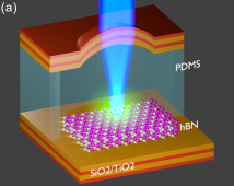
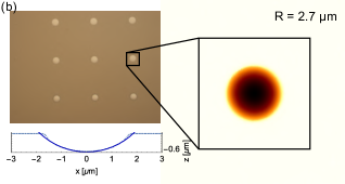
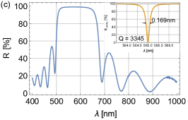
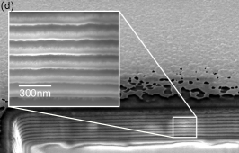
The confocal microcavity consists of a hemispherical and a flat mirror, with the hBN flake hosting the quantum emitter transferred to the focal point of the cavity (see Figure 1(a)). The hemisphere spatially confines the cavity mode to the location of the emitter and is fabricated using I2-enhanced focused ion beam millingDolan et al. (2010); Trichet et al. (2015). We fabricated arrays of 64 hemispheres per substrate with varying geometrical parameters. The surface roughness could be minimized by adding I2-gas during the milling process. With the FIB we can achieve radii of curvature down to m (see Figure 1(b)). We initially characterized the hemispheres using an atomic force microscope (AFM) and phase-shift interferometry (PSI). The characteristic parameters extracted with both methods agree well, which allows us to use the much faster PSI for the characterizations. The hemisphere profile shown in Figure 1(b) has a radius of 2.7m and root mean square deviations nm from an ideal hemispheresup . Note that we did not fabricate full hemispheres and the shapes deviate at the edges (which is due to a conductive coating to prevent charging effects during the milling). Both the flat and concave substrate are coated with 9 pairs of alternating dielectric quarter wave stacks (SiO2/TiO2), deposited using plasma sputtering. We measured a reflectivity of 99.2 at a wavelength of 565 nm (see Figure 1(c)). The calculated resulting cavity reflectivity (see Figure 1(c), small inset) has a FWHM of 0.169 nm, corresponding to a quality factor of . The stopband of the cavity requires the single-photon excitation laser to be shorter than 504 nm, otherwise the cavity has to be resonant at both the ZPL and excitation wavelength. By cutting through one of the stacks with a FIB and imaging with a scanning electron microscope (SEM) in immersion mode (see Figure 1(d)), we see that stacking defects occur, as expected predominantly in higher layers. This is not an issue, however, as they are still . The reflectivity is most likely limited by incorporated residual nitrogen, leading to scattering losses. It should also be noted that at a high magnification (see inset) the stacks show a spotted pattern. This is actually re-deposition of atoms during the milling with the FIB. The backsides of the substrates were coated with anti-reflective coatings, consisting of a single quarter wave layer MgF2. This reduces the reflection losses at the glass-air interface from 4.33 to 2.97.
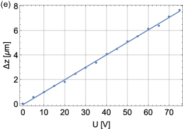
Multilayer hBN flakes have been placed onto the flat mirror via clean polymer transfer (see Methods). The more common direct dry transfer was not used as this usually also transfers residues. The hBN crystals were treated using an oxygen plasma followed by rapid thermal annealing under an Ar atmosphereVogl et al. (2018a). Using plasma etching, defects with their ZPL primarily around 560 nm form, well within the stopband of the coating. Finally, a tuneable polymer spacer is deposited onto the concave mirror. A piezoelectric actuator provides the tuning force and compresses the polymer. In contrast to monolithic cavitiesLiu et al. (2014); Lundt et al. (2016); Knopf et al. (2019), this approach allows for in-situ tuning of the cavity length. The tuning capability is essential, since the exact position of the ZPL cannot yet be controlled and the optical cavity mode has to be artificially matched to the spectrum of the emitterKim et al. (2018). Due to a suitable Young’s modulus and the ability to deform reversibly, we selected PDMS (polydimethylsiloxane) from a range of polymerssup . Figure 1(e) shows that the compression of the PDMS film is linear with the driving voltage at the actuator, with a tuning of 102 nmV-1. This allows us to easily lock the cavity to any arbitrary wavelength. To prevent influence of the PDMS on the emitter, the PDMS was etched around the array.
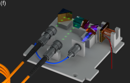
The cavity mirrors, together with all in- and out-coupling optics, were aligned and glued to a monolithic platform (see Figure 1(f) and sup ). Prior to the gluing each component, held with vacuum tweezers, has been aligned with a motorized 6-axis translation stage. This greatly reduces the size of the complete SPS, at the cost of limiting the tuneability to only cavity length. Changing the radius of curvature of the cavity as demonstrated in a similar experiment is thus not possibleFlatten et al. (2018). Nevertheless, the compact size of optics, as well as choice of electronics and excitation laser, allow us to reduce the size of the full experiment to cm3. This is the size requirement of the 1U CubeSat standard, a miniature pico-class satellite. This makes the single-photon source portable and a promising candidate for low cost CubeSat-based single-photon QKD, especially as the quantum ermitters in hBN are space-certifiedVogl et al. (2018b).
III Performance of the single-photon source
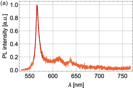
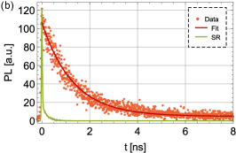
Prior to the cavity experiments we performed a free-space characterization of the quantum emitter on the mirror. All measurements were carried out at room temperature. The defects were located using confocal photoluminescence (PL) mapping under off-resonant excitation at 522 nm. As hBN itself is optically inactive in the visible spectrum, all emission originates from the defects or surface contaminants. Each crystal is scanned with a resolution of 0.5m. For the cavity, we selected a suitable defect with a ZPL at 565.85(5) nm and a Lorentzian linewidth (FWHM) of 5.76(34) nm (see Figure 2(a)). The PL spectrum shows the typical asymmetric lineshape. Note that this is not a result of partial suppression of the long pass filter used to block the pump laser (see Methods), but rather the PSB being adjacent to the ZPL. The defect emits 63.2 into its ZPL. We note that the emission nm originates from surface contaminants activated during the annealing and is usually filtered out (see Methods). Alternatively, annealing in a reactive environment can burn off these contaminants. Time-resolved PL (TRPL) reveals a single-exponential decay with a lifetime of 897(8) ps (see Figure 2(b)). The fit function is convoluted with the system response (also shown in Figure 2(b)) in order to reproduce the observed data.
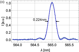
For the cavity experiments we used a custom-built high-resolution Fourier-transform spectrometer (FTS), instead of the grating-based spectrometer. After aligning the concave to the flat mirror and coupling the emitter with the cavity mode, we saw an improved spectral purity (see Figure 2(c)), with the single-photon linewidth narrowing down to 0.224 nm (FWHM). In frequency space this corresponds to 210.6 GHz. The spectrum, however, shows side lobes, which do not originate from higher-order transverse cavity modes. The transverse mode spacing is much larger than the difference in observed peak positionssup . These peaks are artifacts from the finite scan range of the FTS which results in a truncated Fourier-transform. Convoluting this response (which is of the form of ) with a Lorentzian reproduces the observed data.
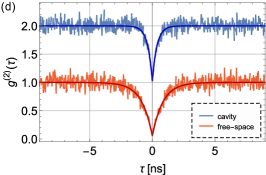
The lifetime cannot be measured directly using time-resolved PL, as the wavelength of the ultra-short pulsed laser is within the stopband of the cavity. For a single-photon emitter, however, it is possible to extract the lifetime directly from the second-order correlation function, which we measure using a Hanbury Brown and Twiss (HBT)-type interferometer. For the emitter in the cavity, we measure (see Figure 2(d)) and from the fit we extract a lifetime of 366(19) ps (see Methods). For a fair comparison of free-space and cavity-enhanced lifetimes we compare the correlation function measurements in free-space and with the cavity. The for the uncoupled emitter dips only to 0.051(23) and has a lifetime of 837(30) ps. The lifetimes measured with time-resolved PL and extracted from the measurements agree reasonably well, even though we note that the 897(8) ps from the TRPL measurement is likely more accurate. While is within the error margin for the cavity-coupled emitter, more accurate measurements are required to reduce the error margin to extract the true value of . Knowing this is crucial for QKD applications (see below). A small error margin on correlation function measurements can typically be achieved with ultra-short pulsed excitationHanschke et al. (2018); Schweickert et al. (2018). We also calculated the background correction termBeveratos et al. (2001) and found that it is smaller than the significant digits of our measurement result (), so we conclude that any deviation from 0 is not due to detector dark counts, but rather other noise sources excited through the laser. If we directly compare of the uncoupled and cavity-enhanced emitter, however, we see a reduction of a factor of 2.83. Such reduction can typically be achieved in the ”bad-emitter” regime and means that off-resonant noise sources are successfully suppressed. A narrower cavity linewidth could thus further reduce . The ratio of free-space (or rather half-sided cavity) to cavity-coupled lifetime is . The effective Purcell enhancement is given by
| (1) |
with being the effective quality factor and being the cavity mode volume. We calculate the mode volume to be 1.76. In the ”bad-emitter” regime the effective quality factor has to be used, which is dominated by the emitter dynamics. It should be mentioned that this is only an approximation and it is more accurate to calculate the overlap integral of the photonic density of states of the cavity and electronic density of states of the emitter. In addition, this effective Purcell factor is different from the ratio , because the dielectric environment of the mirror is modifying the available density of states, whereas the Purcell factor is the ratio of vacuum (or true free-space) to cavity lifetime. We calculate the effective Purcell factor to be 4.07. This also allows for the direct calculation of the quantum efficiencyFlatten et al. (2018), given by
| (2) |
where is the Purcell factor caused by the mirror and is determined by finite-difference time-domain (FDTD) simulations. For our mirror we find sup and thus the quantum efficiency is 51.3.
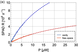
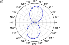
The cavity also modifies the power saturation behavior (see Figure 2(e)), with an increased single-photon count rate even at lower excitation power. This is a result of the Purcell enhancement, which makes the emitter brighter, but also from the increased collection efficiency of the cavity, as the emitter predominantly emits into the cavity mode. The low excitation power also assists the single-photon count rate stability, because at low excitation power the emitters show no blinking or photobleaching. This is particular important as the photobleaching increases with decreasing wavelengthShotan et al. (2016) and due to the stopband of the cavity our excitation laser is at 450 nm. Note that the count rates at the single-photon avalanche diodes (SPADs) shown in Figure 2(e) are the raw count rates, not corrected for transmission loss or detector efficiency. The quantum emitter also emits linearly polarized light (see Figure 2(f)) with a degree of polarization (DOP) of 90.4. The fit is obtained using a function. A high polarization contrast is crucial for QKD applications which use polarization encoding. Increasing the DOP of not fully polarized light is always accompanied by loss, and so it sets an upper bound on the efficiency of the SPS.
Since the cavity length is tuneable, the single-photon wavelength can also be tuned. Effectively, the tuning range is the linewidth of the free-space emission. The cavity is only sampling the free-space emission spectrum, however, so the actual single-photon count rate is the spectral overlap integral of optical cavity mode and emitter. This results in the emission rate decreasing with increasing cavity detuning.
IV Theoretical modeling
IV.1 Numerical modeling
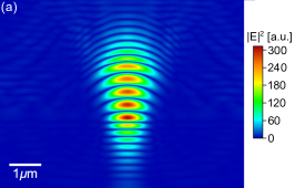
We can use FDTD simulations to calculate the electric field distribution of the dipole emitter in the cavity. The electric field intensity () is shown in Figure 3(a). The simulations also show that resonance does not occur at a physical mirror separation which is a multiple of . This is due to the finite penetration depth of the electric field into the dielectric mirror stacks, leading to an effective cavity length. The penetration depth thereby is given by
| (3) |
The physical mirror separation is determined by maximizing the intracavity electric fieldsup . Our simulations yield nm. When designing the thickness of the PDMS spacer, this has to be taken into account. To reduce the computational time we simulated the longitudinal mode instead of the experimentally realized . Nevertheless, the parameter is not affected by this beyond the numerical precision of the simulation.
IV.2 Applications in quantum technologies
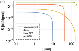
We now turn to an evaluation of the SPS for the two most common quantum information applications: quantum key distribution and quantum computing. Due to the lack of suitable SPSs the vast majority of QKD implementations use weak coherent states (WCSs). These are characterized by a low mean photon number (resulting in a low efficiency of the protocol) and a non-zero probability of emitting two or more photons at the same time. The multi-photon pulses contain information leaking to a potential eavesdropper. This can be reduced at the expense of sacrificing parts of the exchanged key. In comparison, an ideal single-photon source has an efficiency of unity and no multi-photon emission, so it always performs better than any protocol based on WCSs. We assess the performance of our single-photon source for the BB84 protocolGisin et al. (2002) over a fiber channel with a loss of 0.21 dB/km and realistic parameters from the experiment by Gobby, Yuan and Shields (GYS)Gobby et al. (2004). It should be mentioned that such loss can only be achieved at telecom wavelengths, where single-photon emission from hBN has yet to be demonstrated, but for simplicity we still use all GYS parameters. The relevant metric is the extractable secret bit per sent signalsup . Moreover, we compare the results with an ideal SPS and the most common conventional QKD protocols: weak coherent and decoy statesLo et al. (2005). The latter is the most efficient protocol that is publicly known. The simulations for weak coherent and decoy states assume a fixed mean photon number per pulse , however, there is an optimal choice of for every distance.
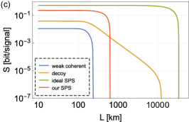
At short and medium distances below 42 km, our SPS outperforms both weak coherent and decoy states, while at long distances decoy states become more efficient (see Figure 3(b)). This is due to the fact that at long distances (i.e. high losses), multi-photon pulses harm the extractable secret bit disproportionately. Nevertheless, our SPS performs better than weak coherent states in each instance. Decoy state protocols can still achieve a finite secret key rate at large distances, because they can extract information from multi-photon states while at the same time defeating the photon-number splitting attack (multi-photon states dominate at long distances with high losses). A communication distance of km would be typical for metropolitan networks. The ideal SPS of course outperforms all protocols and also our source at all distances. For space-to-ground links the loss is dominated by diffraction and atmospheric attenuation plays a role only in the lowest 10 km. The simulations (see Figure 3(c)) show that our source outperforms the decoy state protocol on distances up to 630 km. For a comparison: The Micius satellite, which performed the first satellite-to-ground quantum key exchange, orbits at around 500 kmLiao et al. (2017). Thus, our single-photon source could enhance the key generation rate even with its current performance for such a satellite. We note that the free-space loss channel assumes only diffraction losses and no other noise sources such as pointing errors, atmospheric loss and losses in the transmitter or receiver, which would change the result only marginally. The crossing point where our SPS and the decoy state protocol perform equally efficient for both channels is at a loss of 8.82 dB.
Notably, QKD only requires maximal entropy on all degrees of freedom which are not used for qubit encoding. Other quantum information protocols, however, do require truly indistinguishable single-photons. An example are entangling gates for single-photons for use in one-way quantum computingRaussendorf and Briegel (2001). A measure of how indistinguishable consecutively emitted single-photons are is the interference contrast in a Hong-Ou-Mandel experimentHong et al. (1987). Unfortunately, as our cavity is pumped continuously, we cannot directly measure . Nevertheless, we can at least theoretically calculate the expected indistinguishability. The indistinguishability of a quantum emitter with pure dephasing is given by
| (4) |
where is the emission rate and is the pure dephasing rate. At room temperature we find , meaning only 1 in 5000 photons would interfere in a Hong-Ou-Mandel experiment. Even such a strongly dephasing emitter, however, can reach a regime of high indistinguishability, when coupled with a high-Q cavity. In the limit of weak coupling modifies to
| (5) |
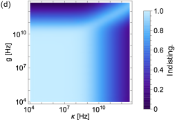
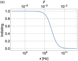
where the parameter is the effective transfer rate between the emitter and the cavity, is the cavity linewidth and is the cavity coupling strengthGrange et al. (2015). For our cavity parameters we find . While this is an improvement by a factor of 26, it is still far beyond being useful for fault-tolerant quantum computing. The indistinguishability for generalized cavity linewidth and coupling strength is shown in Figure 3(d). Note that in the limit of strong coupling it is also possible to achieve a high indistinguishability. With the coupling strength typically GHz, a narrow cavity linewidth is required to maximize . Figure 3(e) shows that requires a cavity linewidth less than 124 MHz. At a reflectivity of Flatten et al. (2018), this linewidth limits the free spectral range (FSR) to 779 GHz. Compared with the free-space emission linewidth (5.41 THz) this means that the spectral profile of the cavity would be comb-shaped, with the cavity sampling the emitter spectrum at multiples of the FSR. Single-photons originating from different comb peaks are of course distinguishable, so a high indistinguishability requires filtering out only one peak (for example with another cavity). This, however, is balanced by a loss in efficiency. To overcome this, the natural linewidth of the emitter into free-space must be narrowed. Cryogenic cooling is one option to narrow the linewidth sufficientlyDietrich et al. (2018).
V Conclusion
We have demonstrated coupling of a quantum emitter hosted by multilayer hBN to a confocal microcavity. The hemispherical geometries have been fabricated using FIB milling with sub-nm precision. The cavity mode volume is of the order of . The cavity improves the spectral purity of the emitter substantially, with the FWHM decreasing from 5.76 to 0.224 nm. Moreover, the cavity suppresses off-resonant noise, which allows us to improve its single-photon purity. The excited state lifetime of the emitter is also shortened by the Purcell effect by a factor of 2.3. The emission of the cavity is linearly polarized and stable over long timeframes, with no signs of photobleaching or blinking. The cavity also features a linearly tunable PDMS spacer between both mirrors, which allows in-situ tuning of the single-photon line over the full free-space ZPL of the quantum emitter. This would allow us to fabricate multiple identical single-photon sources, by locking all to the same emission wavelength, making this approach fully scalable. Furthermore, the complete SPS is portable and fully self-contained within cm3, the size of a 1U CubeSat. This makes the single-photon source a promising candidate for low cost satellite-based long-distance QKD, especially as the quantum emitters in hBN are space-certified. Despite the source’s performance being not yet sufficient for one-way quantum computing, using the single-photon source for QKD even now enhances the quantum key generation rate on useful distances. The microcavity platform can also be easily adapted to other quantum emitters in 2D materials and offers a promising path towards scalable quantum information processing.
Acknowledgements.
This work was funded by the Australian Research Council (CE110001027, FL150100019, DE140100805, DP180103238). We thank the ACT Node of the Australian National Fabrication Facility for access to their nano- and microfabrication facilities. We also thank Hark Hoe Tan for access to the TRPL system. R.L. acknowledges support by an Australian Government Research Training Program (RTP) Scholarship.Appendix: Methods
V.1 FIB milling
Borosilicate glass substrates with a size of have been coated with 100 nm gold using electron-beam thermal evaporation to prevent substrate charging effects. The ion accelerating voltage in the FIB (FEI Helios 600 NanoLab) is 30 kV with currents nA. The dose rate is encoded in the RGB color of a hemispherical pixel map. The dose rate to RGB value was carefully calibrated using AFM measurements. During the milling process we add I2-gas, which ensures a smooth surface. Finally, the gold film is chemically etched using a custom-made potassium iodide (KI:I2:H2O with ratio 4:1:40 by weight) solution. Surface characterizations before and after the KI-etching show no difference in radius or roughness. We also tried hydrofluoric acid to etch the hemispheres, but for the feature sizes required for the cavity we could not achieve a smooth surface.
V.2 Plasma sputtering
We calibrated the deposition rate of the sputter coater (AJA) using variable angle spectroscopic ellipsometry (JA Woollam M-2000D), which measures film thickness and refractive index. At 565 nm we found n, n and n. The deposition was done at room temperature. For the highly reflective coating we deposit alternating layers of SiO2/TiO2 with thickness of and the SiO2 terminating the mirror. Due to the refractive index of MgF2 being roughly in the middle between glass and air, the backsides of the substrates are coated with one quarter wave layer of MgF2, serving as an anti-reflective coating. To maximize the escape efficiency into one particular direction it is common to make one of the stacks thicker (e.g. 10:9), so the photons couple primarily into a single direction. For simplicity, we used 9:9 stacks, which thus introduces 50 loss.
V.3 Quantum emitter fabrication
The flat mirrors have been coated with 300 nm 950 PMMA A4. Multilayer hBN flakes have been exfoliated from bulk (HQGraphene) and transferred onto the PMMA layer by dry contact. Oxygen plasma etching (500 W for 2 min generated from a microwave field at a gas flow of 300 ccm3/min) removes the PMMA around the flake as well as creates the quantum emitters. The PMMA below the flake is decomposed during the annealing, which also stabilizes the optical emission properties (more details have been published previouslyVogl et al. (2018a)).
V.4 Optical characterization
Each flake has been scanned using a custom-built confocal micro-photoluminescence setup with a resolution of m and a spectrum has been recorded at each scanning position. The excitation laser with a wavelength of 522 nm is non-resonant with the optical transition energy of the defect. The laser light is blocked with a Semrock RazorEdge ultrasteep long-pass edge filter. With a laser pulse length of 300 fs at a repetition rate of 20.8 MHz, the setup also allows us to measure the excited state lifetime. The pulses are split into trigger and excitation pulses, and the photoluminescence is detected by a SPAD (Micro Photon Devices). The time correlation between trigger pulse and arrival time of the photoluminescence is given by a time-to-digital converter (PicoQuant PicoHarp 300). The photoluminescence is coupled via a grating to the SPAD, which makes the TRPL wavelength-sensitive. This allows us to measure the lifetime of the ZPL only. The second-order correlation function measurements have been performed using two SPADs in the exit ports of a beam splitter and under continuous excitation. We fit the function
| (6) |
with the anti- and bunching amplitudes and , and the decay times and . The experimental data is normalized such that . The background corrected is given by
| (7) |
with where SNR is the signal-to-noise ratio. In addition to the long-pass filter, the photoluminescence for correlation function measurements is band-pass filtered around the ZPL. We utilize linear variable filters (Delta Optical Thin Film 3G LVLWP and 3G LVSWP) to tune center and bandwidth of the band-pass filtering system.
References
- O’Brien et al. (2009) Jeremy L. O’Brien, Akira Furusawa, and Jelena Vučković, “Photonic quantum technologies,” Nat. Photon. 3, 687–695 (2009).
- Senellart et al. (2017) Pascale Senellart, Glenn Solomon, and Andrew White, “High-performance semiconductor quantum-dot single-photon sources,” Nat. Nanotechnol. 12, 1026–1039 (2017).
- Barros et al. (2009) H. G. Barros, A. Stute, T. E. Northup, C. Russo, P. O. Schmidt, and R. Blatt, “Deterministic single-photon source from a single ion,” New J. of Phys. 11, 103004 (2009).
- Aharonovich et al. (2016) Igor Aharonovich, Dirk Englund, and Milos Toth, “Solid-state single-photon emitters,” Nat. Photon. 10, 631–641 (2016).
- Bock et al. (2016) Matthias Bock, Andreas Lenhard, Christopher Chunnilall, and Christoph Becher, “Highly efficient heralded single-photon source for telecom wavelengths based on a PPLN waveguide,” Opt. Express 24, 23992–24001 (2016).
- Tonndorf et al. (2015) Philipp Tonndorf, Robert Schmidt, Robert Schneider, Johannes Kern, Michele Buscema, Gary A. Steele, Andres Castellanos-Gomez, Herre S. J. van der Zant, Steffen Michaelis de Vasconcellos, and Rudolf Bratschitsch, “Single-photon emission from localized excitons in an atomically thin semiconductor,” Optica 2, 347–352 (2015).
- Srivastava et al. (2015) A. Srivastava, M. Sidler, A. V. Allain, D. S. Lembke, A. Kis, and A. Imamoǧlu, “Optically active quantum dots in monolayer WSe2,” Nat. Nanotechnol. 10, 491–496 (2015).
- Koperski et al. (2015) M. Koperski, K. Nogajewski, A. Arora, V. Cherkez, P. Mallet, J.-Y. Veuillen, J. Marcus, P. Kossacki, and M. Potemski, “Single photon emitters in exfoliated WSe2 structures,” Nat. Nanotechnol. 10, 503–506 (2015).
- He et al. (2015) Y.-M. He, G. Clark, J. R. Schaibley, Y. He, M.-C. Chen, Y.-J. Wei, X. Ding, Q. Zhang, W. Yao, X. Xu, C.-Y. Lu, and J.-W. Pan, “Single quantum emitters in monolayer semiconductors,” Nat. Nanotechnol. 10, 497–502 (2015).
- Chakraborty et al. (2015) C. Chakraborty, L. Kinnischtzke, K. M. Goodfellow, R. Beams, and A. N. Vamivakas, “Voltage-controlled quantum light from an atomically thin semiconductor,” Nat. Nanotechnol. 10, 507–511 (2015).
- Palacios-Berraquero et al. (2016) Carmen Palacios-Berraquero, Matteo Barbone, Dhiren M. Kara, Xiaolong Chen, Ilya Goykhman, Duhee Yoon, Anna K. Ott, Jan Beitner, Kenji Watanabe, Takashi Taniguchi, Andrea C. Ferrari, and Mete Atatüre, “Atomically thin quantum light-emitting diodes,” Nat. Commun. 7, 12978 (2016).
- Branny et al. (2016) Artur Branny, Gang Wang, Santosh Kumar, Cedric Robert, Benjamin Lassagne, Xavier Marie, Brian D. Gerardot, and Bernhard Urbaszek, “Discrete quantum dot like emitters in monolayer MoSe2: Spatial mapping, magneto-optics, and charge tuning,” Appl. Phys. Lett. 108, 142101 (2016).
- Klein et al. (2019) J. Klein, M. Lorke, M. Florian, F. Sigger, J. Wierzbowski, J. Cerne, K. Müller, T. Taniguchi, K. Watanabe, U. Wurstbauer, M. Kaniber, M. Knap, R. Schmidt, J. J. Finley, and A. W. Holleitner, “Atomistic defect states as quantum emitters in monolayer MoS2,” (2019), arXiv:1901.01042, arXiv:1901.01042 .
- Tran et al. (2016a) T. T. Tran, K. Bray, M. J. Ford, M. Toth, and I. Aharonovich, “Quantum emission from hexagonal boron nitride monolayers,” Nat. Nanotechnol. 11, 37–41 (2016a).
- Tran et al. (2016b) Toan Trong Tran, Christopher Elbadawi, Daniel Totonjian, Charlene J. Lobo, Gabriele Grosso, Hyowon Moon, Dirk R. Englund, Michael J. Ford, Igor Aharonovich, and Milos Toth, “Robust multicolor single photon emission from point defects in hexagonal boron nitride,” ACS Nano 10, 7331–7338 (2016b).
- Tran et al. (2016c) Toan Trong Tran, Cameron Zachreson, Amanuel Michael Berhane, Kerem Bray, Russell Guy Sandstrom, Lu Hua Li, Takashi Taniguchi, Kenji Watanabe, Igor Aharonovich, and Milos Toth, “Quantum emission from defects in single-crystalline hexagonal boron nitride,” Phys. Rev. Applied 5, 034005 (2016c).
- Cassabois et al. (2016) G. Cassabois, P. Valvin, and B.Gil, “Hexagonal boron nitride is an indirect bandgap semiconductor,” Nat. Photonics 10, 262–266 (2016).
- Schell et al. (2017) Andreas W. Schell, Hideaki Takashima, Toan Trong Tran, Igor Aharonovich, and Shigeki Takeuchi, “Coupling quantum emitters in 2D materials with tapered fibers,” ACS Photonics 4, 761–767 (2017).
- Vogl et al. (2017) Tobias Vogl, Yuerui Lu, and Ping Koy Lam, “Room temperature single photon source using fiber-integrated hexagonal boron nitride,” J. Phys. D. 50, 295101 (2017).
- Vogl et al. (2018a) Tobias Vogl, Geoff Campbell, Ben C. Buchler, Yuerui Lu, and Ping Koy Lam, “Fabrication and deterministic transfer of high-quality quantum emitters in hexagonal boron nitride,” ACS Photonics 5, 2305–2312 (2018a).
- Kianinia et al. (2017) Mehran Kianinia, Blake Regan, Sherif Abdulkader Tawfik, Toan Trong Tran, Michael J. Ford, Igor Aharonovich, and Milos Toth, “Robust solid-state quantum system operating at 800 K,” ACS Photonics 4, 768–773 (2017).
- Vogl et al. (2018b) T. Vogl, K. Sripathy, A. Sharma, P. Reddy, J. Sullivan, J. R. Machacek, L. Zhang, F. Karouta, B. C. Buchler, M. W. Doherty, Y. Lu, and P. K. Lam, “Radiation tolerance of two-dimensional material-based devices for space applications,” (2018b), arXiv:1811.10138, arXiv:1811.10138 .
- Tawfik et al. (2017) Sherif Abdulkader Tawfik, Sajid Ali, Marco Fronzi, Mehran Kianinia, Toan Trong Tran, Catherine Stampfl, Igor Aharonovich, Milos Toth, and Michael J. Ford, “First-principles investigation of quantum emission from hbn defects,” Nanoscale 9, 13575–13582 (2017).
- Abdi et al. (2018) Mehdi Abdi, Jyh-Pin Chou, Adam Gali, and Martin B. Plenio, “Color centers in hexagonal boron nitride monolayers: A group theory and ab initio analysis,” ACS Photonics 5, 1967–1976 (2018).
- Bourrellier et al. (2016) Romain Bourrellier, Sophie Meuret, Anna Tararan, Odile Stéphan, Mathieu Kociak, Luiz H. G. Tizei, and Alberto Zobelli, “Bright UV single photon emission at point defects in h-BN,” Nano Lett. 16, 4317–4321 (2016).
- Shotan et al. (2016) Zav Shotan, Harishankar Jayakumar, Christopher R. Considine, Mažena Mackoit, Helmut Fedder, Jörg Wrachtrup, Audrius Alkauskas, Marcus W. Doherty, Vinod M. Menon, and Carlos A. Meriles, “Photoinduced modification of single-photon emitters in hexagonal boron nitride,” ACS Photonics 3, 2490–2496 (2016).
- Chejanovsky et al. (2016) Nathan Chejanovsky, Mohammad Rezai, Federico Paolucci, Youngwook Kim, Torsten Rendler, Wafa Rouabeh, Felipe Fávaro de Oliveira, Patrick Herlinger, Andrej Denisenko, Sen Yang, Ilja Gerhardt, Amit Finkler, Jurgen H. Smet, and Jörg Wrachtrup, “Structural attributes and photodynamics of visible spectrum quantum emitters in hexagonal boron nitride,” Nano Lett. 16, 7037–7045 (2016).
- Xu et al. (2018) Zai-Quan Xu, Christopher Elbadawi, Toan Trong Tran, Mehran Kianinia, Xiuling Li, Daobin Liu, Timothy B. Hoffman, Minh Nguyen, Sejeong Kim, James H. Edgar, Xiaojun Wu, Li Song, Sajid Ali, Mike Ford, Milos Toth, and Igor Aharonovich, “Single photon emission from plasma treated 2D hexagonal boron nitride,” Nanoscale 10, 7957–7965 (2018).
- Choi et al. (2016) Sumin Choi, Toan Trong Tran, Christopher Elbadawi, Charlene Lobo, Xuewen Wang, Saulius Juodkazis, Gediminas Seniutinas, Milos Toth, and Igor Aharonovich, “Engineering and localization of quantum emitters in large hexagonal boron nitride layers,” ACS Appl. Mater. Interfaces 8, 29642–29648 (2016).
- Ngoc My Duong et al. (2018) Hanh Ngoc My Duong, Minh Anh Phan Nguyen, Mehran Kianinia, Takeshi Ohshima, Hiroshi Abe, Kenji Watanabe, Takashi Taniguchi, James H. Edgar, Igor Aharonovich, and Milos Toth, “Effects of high-energy electron irradiation on quantum emitters in hexagonal boron nitride,” ACS Appl. Mater. Interfaces 10, 24886–24891 (2018).
- Proscia et al. (2018) Nicholas V. Proscia, Zav Shotan, Harishankar Jayakumar, Prithvi Reddy, Charles Cohen, Michael Dollar, Audrius Alkauskas, Marcus Doherty, Carlos A. Meriles, and Vinod M. Menon, “Near-deterministic activation of room-temperature quantum emitters in hexagonal boron nitride,” Optica 5, 1128–1134 (2018).
- Gisin et al. (2002) Nicolas Gisin, Grégoire Ribordy, Wolfgang Tittel, and Hugo Zbinden, “Quantum cryptography,” Rev. Mod. Phys. 74, 145–195 (2002).
- Kok et al. (2007) Pieter Kok, W. J. Munro, Kae Nemoto, T. C. Ralph, Jonathan P. Dowling, and G. J. Milburn, “Linear optical quantum computing with photonic qubits,” Rev. Mod. Phys. 79, 135–174 (2007).
- Vahala (2003) Kerry J. Vahala, “Optical microcavities,” Nature 424, 839–846 (2003).
- Kaupp et al. (2013) Hanno Kaupp, Christian Deutsch, Huan-Cheng Chang, Jakob Reichel, Theodor W. Hänsch, and David Hunger, “Scaling laws of the cavity enhancement for nitrogen-vacancy centers in diamond,” Phys. Rev. A 88, 053812 (2013).
- Iff et al. (2018) Oliver Iff, Nils Lundt, Simon Betzold, Laxmi Narayan Tripathi, Monika Emmerling, Sefaattin Tongay, Young Jin Lee, Soon-Hong Kwon, Sven Höfling, and Christian Schneider, “Deterministic coupling of quantum emitters in WSe2 monolayers to plasmonic nanocavities,” Opt. Express 26, 25944–25951 (2018).
- Luo et al. (2018) Yue Luo, Gabriella D. Shepard, Jenny V. Ardelean, Daniel A. Rhodes, Bumho Kim, Katayun Barmak, James C. Hone, and Stefan Strauf, “Deterministic coupling of site-controlled quantum emitters in monolayer WSe2 to plasmonic nanocavities,” Nat. Nanotechnol. 13, 1137–1142 (2018).
- Flatten et al. (2018) L. C. Flatten, L. Weng, A. Branny, S. Johnson, P. R. Dolan, A. A. P. Trichet, B. D. Gerardot, and J. M. Smith, “Microcavity enhanced single photon emission from two-dimensional WSe2,” Appl. Phys. Lett. 112, 191105 (2018).
- Tran et al. (2017) Toan Trong Tran, Danqing Wang, Zai-Quan Xu, Ankun Yang, Milos Toth, Teri W. Odom, and Igor Aharonovich, “Deterministic coupling of quantum emitters in 2d materials to plasmonic nanocavity arrays,” Nano Lett. 17, 2634–2639 (2017).
- Kim et al. (2018) Sejeong Kim, Johannes E. Fröch, Joe Christian, Marcus Straw, James Bishop, Daniel Totonjian, Kenji Watanabe, Takashi Taniguchi, Milos Toth, and Igor Aharonovich, “Photonic crystal cavities from hexagonal boron nitride,” Nat. Commun. 9, 2623 (2018).
- Liao et al. (2017) Sheng-Kai Liao, Wen-Qi Cai, Wei-Yue Liu, Liang Zhang, Yang Li, Ji-Gang Ren, Juan Yin, Qi Shen, Yuan Cao, Zheng-Ping Li, Feng-Zhi Li, Xia-Wei Chen, Li-Hua Sun, Jian-Jun Jia, Jin-Cai Wu, Xiao-Jun Jiang, Jian-Feng Wang, Yong-Mei Huang, Qiang Wang, Yi-Lin Zhou, Lei Deng, Tao Xi, Lu Ma, Tai Hu, Qiang Zhang, Yu-Ao Chen, Nai-Le Liu, Xiang-Bin Wang, Zhen-Cai Zhu, Chao-Yang Lu, Rong Shu, Cheng-Zhi Peng, Jian-Yu Wang, and Jian-Wei Pan, “Satellite-to-ground quantum key distribution,” Nature 549, 43–47 (2017).
- Dolan et al. (2010) Philip R. Dolan, Gareth M. Hughes, Fabio Grazioso, Brian R. Patton, and Jason M. Smith, “Femtoliter tunable optical cavity arrays,” Opt. Lett. 35, 3556–3558 (2010).
- Trichet et al. (2015) Aurélien A. P. Trichet, Philip R. Dolan, David M. Coles, Gareth M. Hughes, and Jason M. Smith, “Topographic control of open-access microcavities at the nanometer scale,” Opt. Express 23, 17205–17216 (2015).
- (44) See Supplemental Material at [URL will be inserted by publisher] for details on hemisphere fabrication, spin speed curves of the PDMS solution, photographs of the device, transverse mode spacing, FDTD simulations and QKD simulations.
- Liu et al. (2014) Xiaoze Liu, Tal Galfsky, Zheng Sun, Fengnian Xia, Erh-chen Lin, Yi-Hsien Lee, Stéphane Kéna-Cohen, and Vinod M. Menon, “Strong light-matter coupling in two-dimensional atomic crystals,” Nat. Photon. 9, 30–34 (2014).
- Lundt et al. (2016) Nils Lundt, Sebastian Klembt, Evgeniia Cherotchenko, Simon Betzold, Oliver Iff, Anton V. Nalitov, Martin Klaas, Christof P. Dietrich, Alexey V. Kavokin, Sven Höfling, and Christian Schneider, “Room-temperature tamm-plasmon exciton-polaritons with a WSe2 monolayer,” Nat. Commun. 7, 13328 (2016).
- Knopf et al. (2019) Heiko Knopf, Nils Lundt, Tobias Bucher, Sven Höfling, Sefaattin Tongay, Takashi Taniguchi, Kenji Watanabe, Isabelle Staude, Ulrike Schulz, Christian Schneider, and Falk Eilenberger, “Integration of atomically thin layers of transition metal dichalcogenides into high-Q, monolithic Bragg-cavities: an experimental platform for the enhancement of the optical interaction in 2D-materials,” Opt. Mater. Express 9, 598–610 (2019).
- Hanschke et al. (2018) Lukas Hanschke, Kevin A. Fischer, Stefan Appel, Daniil Lukin, Jakob Wierzbowski, Shuo Sun, Rahul Trivedi, Jelena Vučković, Jonathan J. Finley, and Kai Müller, “Quantum dot single-photon sources with ultra-low multi-photon probability,” npj Quantum Inf. 4, 43 (2018).
- Schweickert et al. (2018) Lucas Schweickert, Klaus D. Jöns, Katharina D. Zeuner, Saimon Filipe Covre da Silva, Huiying Huang, Thomas Lettner, Marcus Reindl, Julien Zichi, Rinaldo Trotta, Armando Rastelli, and Val Zwiller, “On-demand generation of background-free single photons from a solid-state source,” Appl. Phys. Lett. 112, 093106 (2018).
- Beveratos et al. (2001) Alexios Beveratos, Rosa Brouri, Thierry Gacoin, Jean-Philippe Poizat, and Philippe Grangier, “Nonclassical radiation from diamond nanocrystals,” Phys. Rev. A 64, 061802 (2001).
- Gobby et al. (2004) C. Gobby, Z. L. Yuan, and A. J. Shields, “Quantum key distribution over 122 km of standard telecom fiber,” Appl. Phys. Lett. 84, 3762–3764 (2004).
- Lo et al. (2005) Hoi-Kwong Lo, Xiongfeng Ma, and Kai Chen, “Decoy state quantum key distribution,” Phys. Rev. Lett. 94, 230504 (2005).
- Raussendorf and Briegel (2001) Robert Raussendorf and Hans J. Briegel, “A one-way quantum computer,” Phys. Rev. Lett. 86, 5188–5191 (2001).
- Hong et al. (1987) C. K. Hong, Z. Y. Ou, and L. Mandel, “Measurement of subpicosecond time intervals between two photons by interference,” Phys. Rev. Lett. 59, 2044–2046 (1987).
- Grange et al. (2015) Thomas Grange, Gaston Hornecker, David Hunger, Jean-Philippe Poizat, Jean-Michel Gérard, Pascale Senellart, and Alexia Auffèves, “Cavity-funneled generation of indistinguishable single photons from strongly dissipative quantum emitters,” Phys. Rev. Lett. 114, 193601 (2015).
- Dietrich et al. (2018) A. Dietrich, M. Bürk, E. S. Steiger, L. Antoniuk, T. T. Tran, M. Nguyen, I. Aharonovich, F. Jelezko, and A. Kubanek, “Observation of fourier transform limited lines in hexagonal boron nitride,” Phys. Rev. B 98, 081414 (2018).