Trapping dipolar exciton fluids in GaN/(AlGa)N nanostructures
Abstract
Dipolar excitons offer a rich playground for both design of novel optoelectronic devices and fundamental many-body physics. Wide GaN/(AlGa)N quantum wells host a new and promising realization of dipolar excitons. We demonstrate the in-plane confinement and cooling of these excitons, when trapped in the electrostatic potential created by semitransparent electrodes of various shapes deposited on the sample surface. This result is a prerequisite for the electrical control of the exciton densities and fluxes, as well for studies of the complex phase diagram of these dipolar bosons at low temperature.
keywords:
exciton fluid, electrostatic traps, cooling, gallium nitrideUM] L2C, University of Montpellier, CNRS, Montpellier, France CHREA] CRHEA, Université Côte d’Azur, CNRS, Valbonne, France CHREA] CRHEA, Université Côte d’Azur, CNRS, Valbonne, France CHREA] CRHEA, Université Côte d’Azur, CNRS, Valbonne, France UM] L2C, University of Montpellier, CNRS, Montpellier, France
Dipolar excitons, Coulomb-bound but spatially separated electron-hole pairs, have a long life-time and a built-in dipole moment that offer an opportunity for the cooling and electrical control of exciton fluids 1, 2, 3, 4, 5, 6, 7. Various intriguing quantum phenomena including Bose-Einstein-like condensation, darkening and superfluidity of excitons have been recently reported 8, 9, 10, 11, 12, 13, 14, 15. Albeit demonstrated at very low temperatures, those phenomena are promising for better understanding of new states of matter, but also for potential applications in excitonic devices with novel functionalities 7.
The recent emergence of high quality wide-bandgap semiconductor quantum wells (QWs) and two-dimensional Van der Waals heterostructures, hosting dipolar excitons with large exciton binding energies and built-in electric fields, has given a new impetus to this research 16, 17, 18, 19, 20. Room temperature exciton transport in GaN/(AlGa)N QWs has been demonstrated 17, as well as its electrical control in MoSWSe2 heterostructures 20. The latter is particularly important in the quest for exciton-based efficient interconnects between optical data transmission and electrical processing systems 7.
However, as demonstrated in GaAs-based QWs, trapping, cooling and control of the density of dipolar excitons is essential to address various collective states, such as Bose-Einstein-like condensates, that may form at low temperatures 12, 13. While excitons in GaN-based nanostructures have relatively high binding energies and small Bohr radii 21 (as compared to GaAs-based structures) and thus could exhibit quantum properties at higher temperatures 22, the additional challenges that must be faced to achieve such degree of control are numerous. These may include nonradiative losses 23, megavolt per centimeter-strong built-in electric fields 24, an exponential dependence of the lifetime on the exciton density under high excitation conditions25, 26, 27, and the guided-and-scattered light that must be distinguished from the exciton photoluminescence (PL) 28, 17.
In this letter we overcome those challenges and report on the realization of m m-size thermalized exciton fluid, trapped in the plane of a GaN/(GaAl)N quantum well grown on a free-standing GaN substrate. Our objective is to obtain an area uniformly filled with excitons, with a density that can be controlled by the excitation power. To this end we fabricate electrostatic traps of various shapes by depositing semi-transparent metallic layers on top of the semiconductor nanostructure. Such strategy has already been used in GaAs-based heterostructures 3, 29, but here it has to be adapted to the case of strongly polar heterostructures.
Indeed, in GaN/(AlGa)N heterostructures the built-in electric field due to spontaneous and piezoelectric polarization is of order of megavolt per centimeter 30, 31, 24. It pushes electrons and holes towards the two opposite interfaces of the QW. An exciton consisting of an electron and a hole spatially separated along the growth direction presents a permanent dipolar moment, roughly given by the QW width. The quantum confined Stark effect is so strong that the ground state exciton energy ( in Fig. 1 (a)) is lower (in this work by meV) than that of the exciton energy in bulk GaN. The thin semitransparent metallic layer deposited on top of the structure reduces the electric field in the QW underneath, increasing exciton ground state energy: in Fig. 1 (a). Using this effect, the energy of the exciton can be modulated, making possible the on-demand patterning of the in-plane potential for the QW excitons. Note that this trapping scheme is opposite to the one previously developed in GaAs QWs, where excitons are trapped in the regions covered by the metal, where the electric field is the strongest.
We also compare various sizes and shapes of the electrodes and show that quasi-one-dimensional linear traps are optimal host structures for the exciton fluids (Fig. 1 (b)). They allow us to avoid the dilution of the exciton fluid due to radial extension, and thus to achieve high exciton densities as far as m away from the excitation spot. Moreover, in this geometry, the relative contribution of the parasitic guided-and-scattered light (which is not confined by the electrodes so that its intensity decreases as , where is the distance from the excitation spot) is substantially reduced with respect to the confined excitons emission. Finally, implementation of quasi-one-dimensional zigzag-shaped potential (Fig. 1 (c)) provides unambiguous evidence of the diffusive transport of the trapped excitons.
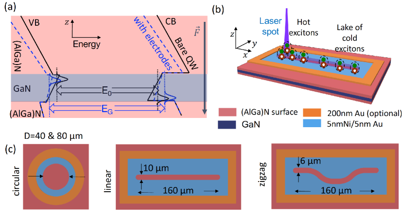
We investigate a nm-wide GaN QW sandwiched between (top) and nm-wide (bottom) AlGa0.89N barriers, grown on a free-standing GaN substrate (LUMILOG, threading dislocation density cm-2 ). The exciton radiative lifetime in such structure (in the zero zero-density limit) is estimated as s 17, exciton binding energy as meV and the built-in electric field kV/cm. The semi-transparent electrodes consisting of nm of Au on top of nm of Ni are evaporated on the sample surface and patterned by optical lithography. Some of the patterns are additionally covered by a nm-thick Au layer for subsequent wire bonding (Fig. 1 (b)). This layer is opaque, but is not expected not affect the surface potential created by the NiAu electrodes. Three electrode geometries used to create in-plane trapping potential are illustrated in Fig. 1 (c): circular trap, linear trap, and zigzag-shaped trap. In contrast with GaAs-based devices, the regions with bare surface are those where the electric field is the strongest, and where excitons accumulate due to maximised confinement, while under the electrodes the field is lower. The details on the calculation of the band profiles and the confinement energies using coupled Schrödinger and Poisson equations are provided in Supporting information. These calculations yield a trapping potential meV, in excellent agreement with experimental results, as shown below. Here and are the exciton energies in the bare QW and in the QW covered by the electrodes, respectively, see Fig. 1 (a).
In most of our experiments the sample is cooled down to K and the QW excitons are created within a m-diameter spot on the sample surface. We use either continuous wave (CW) optical pumping at nm, or quasi-CW pumping at nm (picosecond pulses at MHz frequency, much higher than inverse exciton lifetime MHz) . The PL spectra are acquired by a charge coupled device (CCD) camera with m spatial resolution. More details can be found in Fedichkin et al. 17 and in Supporting information.
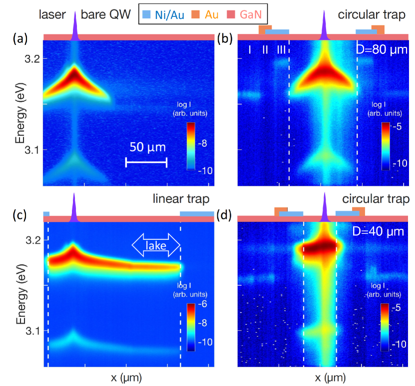
The exciton transport and trapping, as well as their dependence on the trap geometry, are presented in Fig. 2. It shows color-encoded PL spectra, measured at various distances from the excitation spot along the -axis (cf Fig. 1 (b)). The emission from the bare surface (Fig. 2 (a), no trapping electrodes) is compared to the circular traps with diameters m and m (Fig. 2 (b), (d), circular traps) and quasi-one-dimensional channel ( Fig. 2 (c), linear trap). Apart from the broad emission directly under the excitation point, at any distance from the spot the spectrum exhibits two main peaks: the zero-phonon exciton emission line and the first phonon replica meV below 32. The energy, intensity, and linewidth of the excitonic PL decrease when moving away from the excitation position. These effects are due to the screening of the electric field along the growth direction induced by the photocreated carriers: the highest density under the pumping spot corresponds to the maximum screening (lowest electric field), and thus to the highest emission intensity and energy 25, 28, 17. The pump-induced emission energy shift is referred to as the blue shift, . Its magnitude roughly corresponds to the repulsive interaction between the dipolar excitons. can be used for estimating the exciton density as , where eV cm-2 is the coefficient extracted from the self-consistent solution of the Schrödinger and Poisson equations (see also Supporting information) 25, 28, 17. This estimate could be improved taking into account excitonic correlations (see discussion below) 33, 34, 22.
Let us compare the spatial profiles of the emission from the bare QW and circular traps. In the bare sample an arrow-shaped pattern with m-width is accompanied by weak emission far away from the spot at an approximately constant energy of eV, as previously observed in similar samples 17. In the sample with m circular trap an arrow-shaped pattern of similar size can be identified. This means that we load the trap with excitons, but the density across the trap is not homogeneous. By contrast, in a smaller trap, the arrow-shaped pattern is replaced by a flat pattern. This suggests that the in-plane potential is completely screened by the trapped excitons, or, in other words, that the trap is fully filled.
In both circular traps we observe weak, but clearly patterned emission from the outer regions of the trap. Three different zones can by distinguished outside the trap: bare QW (I), thick gold electrode (II) and semitransparent electrode (III). The emission from the zone I is centered at the energy of the empty QW. The excitons that emit this light have escaped from the trap and propagated diffusively, their density is small enough to produce no measurable blue shift. This emission is alike the emission in a bare sample more than m away from the spot. The small difference in the energy between the bare sample ( eV in panel (a)) and the ”outside the trap” zone I ( eV in panels (b) and (d)) could be due to electrostatic effects induced by closely lying electrodes. In the smaller circular trap one can also see in zone I an emission at the same energy as the strongest emission at the center of the trap ( eV). It is alike broad emission in bare sample at more than m from the spot. This light is emitted by the excitons in the trap, guided along the sample plane over tens of microns, and then scattered out of the sample by surface roughness. Indeed, this emission is also present in zone II, where opaque gold electrode impedes any emission that originates from the QW, independently on the size of the trap. Finally, the emission in zone III, the closest to the trap, provides an estimation of the trap depth. This is particularly clear for the m-wide trap. A few excitons that escaped from the trap in the region covered by the semitransparent electrodes emit light at eV. This corresponds to the modulation of the confinement potential induced by the metallic gates. Remarkably, the measured trapping potential meV matches perfectly the value expected from the model based on the solution of the coupled Schrödinger and Poisson equations (see Supporting Information).
The advantage of the linear trap with respect to the circular one is quite natural: it allows us to eliminate the radial dilution of the exciton density (distance), and thus to keep relatively high densities of excitons at significant distances from the excitation spot. Moreover, in circular traps, as well as in the bare QW, the exciton emission competes with the guided-and-scattered light (although these two kinds of emissions can be spectrally distinguished). By contrast, in the linear traps the guided-and-scattered light is subject to the radial dilution, while the excitons are confined in the trap, which is quasi-one-dimensional.
The linear trap (Fig. 2 (c)) exhibits a particularly remarkable emission pattern. While close to the excitation spot one can still distinguish an arrow-shaped pattern, starting from m and further away from the excitation spot the emission energy and intensity are almost independent of the position. This suggests that we have created, within the trap, an area homogeneously filled with carriers, that will be referred to as an exciton lake. At W used in Fig. 2 (c), the blue shift of the exciton energy in the lake does not exceed meV. This is less than the trapping potential, making possible the accumulation of the excitons in the trap.
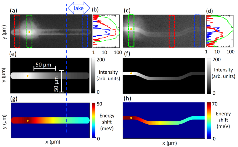
More insight into exciton in-plane propagation and trapping can be obtained from the spectrally integrated emission intensity maps shown in Fig. 3 (a) and (c) for linear and zigzag-shaped traps, respectively. These images are acquired through a CMOS camera after a spectral filter matching the energy range shown in Fig. 2. Two main features can be distinguished in these images. First, along the -direction the emission from the traps is inhomogeneous. The emission from the borders is stronger than the one from the center of the trap. This is additionally illustrated in Fig. 3 (b) and (d), where we show the profiles taken under the spot (green line) and at two other positions along the -direction (red and blue lines) for linear and zigzag-shaped traps, respectively. The observed inhomogeneity is probably related to the shape of the trap, suggesting that the electric field in -direction varies progressively between the in-plane regions covered by the metal and the regions with bare surface.
Second, under the pumping power used in this particular experiment (mW) the traps are strongly leaking. Indeed, the laser spot (position indicated by the yellow dot) is surrounded by a circular halo, suggesting that under the spot the carrier density is high enough to screen the trapping potential meV. This halo being radially symmetric, it may include contribution from the photon diffusion, analogous to the one in Fig. 2 (a). However, the in-plane profiles of the emission in the remote regions of the traps are inconsistent with the radial symmetry of the light propagation. This is particularly obvious from the zigzag-shaped trap emission. Thus, these experiments prove unambiguously that the emission as far as m away from the excitation spot results from the exciton transport, rather than from photon diffusion.
To go further and quantify relevant parameters of the exciton propagation, we apply the exciton transport model developed in Rapaport et al. 35, Fedichkin et al. 17 to the case of transport in a two-dimensional trapping potential. For the sake of simplicity, we neglect some experimentally observed features: we assume infinite trap barriers (no leakage) and spatially homogeneous potential within the trap. The exciton transport is assumed to be limited by the presence of randomly distributed scatterers (Model C of Ref. 17) so that the diffusion coefficient is given by , where is the exciton mass, is the Boltzmann constant, is the free electron mass, and nm is the exciton scattering length. The latter, together with the fraction of the photons absorbed in the QW are the only fitting parameters. The details on the transport modelling are given in the Supporting Information. The results of the numerical solution of the diffusion equation are shown in Fig. 3 (e-h) for both linear (e, g) and zigzag-shaped (f, h) traps. The simulation reproduces the propagation and filling of the traps, as well as the formation of the region m away from the laser spot, where exciton emission energy and intensity are almost constant: the exciton lake.
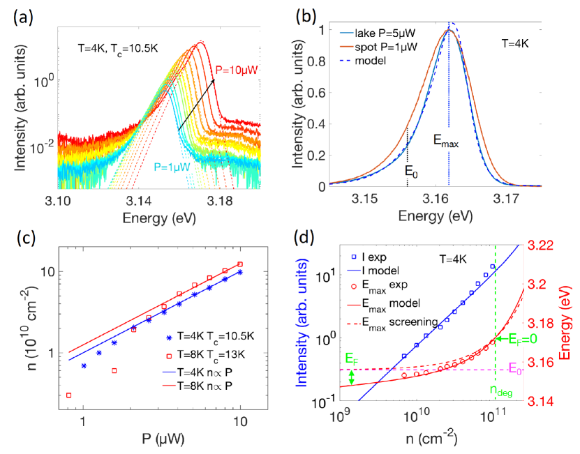
In the following we analyze the spectral properties of the emission from the lake region in the linear trap as a function of excitation power density, in order to demonstrate density and temperature control of the dipolar excitons. Figure 4 (a) shows a set of exciton emission spectra (solid lines) averaged over the lake region of the linear trap (white arrow in Fig. 2 (c)). The power varies from to W and sample temperature is fixed at K. One can identify a blue shift of the emission line ( meV) and increasing intensity that accompanies the increase of the power. The line shape is not Gaussian, as one could expect for the emission dominated by inhomogeneous broadening. Instead, an exponential shape of both high- and low-energy tails is apparent. Similar profiles have already been observed in PL spectra of dipolar excitons 36, 10. In particular, Schinner et al use Fermi-Dirac distribution as a cutoff function, to account for the thermal smearing of the filling of the trap with the dipolar exciton liquid 10. An argument that can be put forward in favor of this approach is that in the case of the bosonic dipolar liquid, the strong spatial dipolar repulsion plays the role of the Pauli principle in the Fermi-Dirac distribution. To account for the inhomogeneous broadening and describe the low-energy tail of the spectrum, Schinner et al multiply the Fermi-Dirac distribution by a phenomenological Gaussian function 10. In our samples the low-energy tail of the excitonic emission is rather exponential, similar to Stern et al. 36 Therefore we model this peculiar shape with the product of the exponential function (to describe the low-energy tail of the spectrum) and the Fermi-Dirac distribution (to account for the temperature-broadened steep decrease of the high-energy tail of the spectrum)111We limit ourselves to the fundamental electronic transition involved in the A-exciton, because we do not observe any evidence of the distinct emission of neither excited states exciton states, nor B-exciton, the emission linewidth meV being of the same order of magnitude as the typical splitting between A and B excitons..
The efficiency of the exciton cooling in the lake can be estimated by fitting this function to the set of data at different powers, as shown in Fig. 4 (a). From such a procedure, we extract the following fitting parameters: the zero-density exciton energy eV, the carrier densities , and the carrier temperature K. The latter appears to be power independent, albeit different from the nominal sample temperature K. The resulting carrier densities are shown in Fig. 4 (c) as a function of the laser power for two sets of data at different nominal temperatures. For K we get K and for K we get K. We speculate that the difference between carrier temperature and the nominal lattice temperature results from the poor thermalization of the crystal lattice in the cold finger cryostat, and the real lattice temperature is higher, so that . Apart from the very lowest powers ( W, where nonradiative recombination may dominate over the radiative one), the carrier density increases linearly with power, indicating vanishing contribution of nonradiative losses. The higher density at higher temperature is a signature of the increasing exciton lifetime in the QW 37.
It is instructive to compare the emission peak with a given energy measured in the lake ( W), and directly at the excitation spot, but at lower power, W. Remarkably, even at a factor of lower excitation power, the emission under the spot is broader than the one in the lake and does not have the same profile, so that the fitting procedure used for the lake spectra is not viable. This suggests that the impact of optical excitation goes beyond the heating of the exciton gas and the screening of the built-in electric field, that are both taken into account by the model.
The determination of the carrier density in the nanostructures hosting dipolar excitons is a very delicate question since it relies on the knowledge of the exciton-exciton interactions. The values of given in Fig. 4 (c-d) are obtained in the rough semi-phenomenological approximation described above, neglecting excitonic correlations: , where is deduced from the self-consistent solution of the Schrödinger and Poisson equations. The same approximation was used in Refs. 28, 17, and it is conceptually similar to the plate capacitor model 38, 39. The effect of the exciton-exciton interactions was investigated theoretically and experimentally in Refs. 33, 34, 40, 41, 42 and results in a density and temperature-dependent correction factor that leads to the underestimation of the density by up to one order of magnitude at the lowest powers and temperatures. Nevertheless, it is not straightforward to apply those considerations to our system, and a more advanced analysis of the data remains to be done. In this work we determine the lower limit for the carrier density, and bear in mind that excitonic correlations may increase it by up to a factor of .
Fig. 4 (d) summarizes the results of the modelling. Both energy (red circles, right scale) and integrated intensity (blue circles, left scale) of the excitonic emission are shown as a function of the exciton density extracted from the model (solid lines). This representation allows us to appreciate the role of the two density-induced contributions to the shift of the emission energy: the screening of the built-in electric field (, red dashed line) and the phase space filling that leads to an additional shift of the emission energy. The latter can be described in terms of the variation of the Fermi energy , that appears in Fig. 4 (d) as the difference between the red solid line, showing the full model and red dashed line, showing the screening effect on the emission energy. One can see that the Fermi contribution is not negligible at low densities, at least within the approximations described above. Importantly, even at maximum carrier densities achieved in the lake the carriers remain in the non-degenerate limit cm-2 ( so that ) and well below exitonic Mott transition expected to occur progressively above cm-2 43. Moreover, the integrated emission intensity is well described by the model, and it increases almost linearly with the exciton density, at least up to W. This means that here the carrier densities are low enough, so that exciton radiative emission rate does not grow exponentially with density, as it is usually observed in polar heterostructures 25, 28, 17, 16, 26, 27.
In conclusion, we have shown that dipolar excitons can be efficiently trapped in the plane of GaN/(AlGa)N QWs. In previous works on GaN QWs hosting dipolar excitons, the mutual repulsion of excitons led to a fast radial expansion and dilution of the exciton gas, accompanied by dramatic variation of the exciton energy and lifetime 28, 17. Here we overcome these problems, and create spatial areas (referred to as lakes) with tens of micrometers characteristic size, homogeneously filled with excitons with well-defined emission energy and lifetime. We show that the exciton fluid trapped in the lake is at macroscopic thermodynamical equilibrium with well-defined temperature close to the sample temperature. The density of this cold exciton fluid can be controlled by changing the laser excitation power.
The realisation of traps relies on the deposition of metallic gates on the surface. Both the electrode shape, and the characteristic electric fields that must be manipulated (of order of MV/cm) are quite different from the known GaAs-based nanostructures. Such strong built-in electric field in nitride-based structures could be not only a challenge to meet, but also an opportunity to avoid spurious photocurrents that limit exciton mobility and coherence properties. These photocurrents are not easy to avoid in other materials hosting dipolar excitons (either GaAs-based or Van der Waals heterostructures), where a voltage must be applied across the regions where excitons accumulate. High exciton binding energy in wide band gap semiconductors, such as GaN and ZnO, make them potentially promising for the realisation of exciton-based optoelectronic devices operating at room temperature. Our results pave the way towards such functionalities, although the electrical control of the exciton fluxes remains to be demonstrated. Finally, the detailed spectroscopic study of dipolar exciton fluids at various densities made possible by the presented results, may shed new light on their intriguing properties, such as macroscopic coherence and condensation, predicted to show up in GaN QWs at higher temperatures than in GaAs.
The authors thanks D. Scalbert for enlightening discussions. This work was supported by the French National Research Agency (ANR OBELIX).
Experimental methods; Modelling of the density-dependent confinement potential and carrier wavefunctions by self-consistent solution of the Schrödinger and Poisson equations; Drift-diffusion modelling for the exciton transport; Modelling of the PL spectra, estimation of the carrier density.
References
- Yudson and Lozovik 1976 Yudson, V. I.; Lozovik, Y. E. A new mechanism for superconductivity: pairing between spatially separated electrons and holes. Soviet Physics JETP 1976, 44, 389
- Miller et al. 1985 Miller, D. A. B.; Chemla, D. S.; Damen, T. C.; Gossard, A. C.; Wiegmann, W.; Wood, T. H.; Burrus, C. A. Electric-Field Dependence of Optical-Absorption Near the Band-Gap of Quantum-Well Structures. Phys. Rev. B 1985, 32, 1043–1060
- Huber et al. 1998 Huber, T.; Zrenner, A.; Wegscheider, W.; Bichler, M. Electrostatic Exciton Traps. physica status solidi (a) 1998, 166, R5–R6
- Ivanov et al. 1999 Ivanov, A. L.; Littlewood, P. B.; Haug, H. Bose-Einstein statistics in thermalization and photoluminescence of quantum-well excitons. Phys. Rev. B 1999, 59, 5032–5048
- Butov et al. 1999 Butov, L. V.; Shashkin, A. A.; Dolgopolov, V. T.; Campman, K. L.; Gossard, A. C. Magneto-optics of the spatially separated electron and hole layers in GaAs/AlxGa1-xAs coupled quantum wells. Phys. Rev. B 1999, 60, 8753–8758
- High et al. 2008 High, A. A.; Novitskaya, E. E.; Butov, L. V.; Hanson, M.; Gossard, A. C. Control of exciton fluxes in an excitonic integrated circuit. Science 2008, 321, 229–231
- Butov 2017 Butov, L. V. Excitonic devices. Superlattices and Microstructures 2017, 108, 2–26
- High et al. 2012 High, A. A.; Leonard, J. R.; Hammack, A. T.; Fogler, M. M.; Butov, L. V.; Kavokin, A. V.; Campman, K. L.; Gossard, A. C. Spontaneous coherence in a cold exciton gas. Nature 2012, 483, 584–588
- Shilo et al. 2013 Shilo, Y.; Cohen, K.; Laikhtman, B.; West, K.; Pfeiffer, L.; Rapaport, R. Particle correlations and evidence for dark state condensation in a cold dipolar exciton fluid. Nature Communications 2013, 4, 1–7
- Schinner et al. 2013 Schinner, G. J.; Repp, J.; Schubert, E.; Rai, A. K.; Reuter, D.; Wieck, A. D.; Govorov, A. O.; Holleitner, A. W.; Kotthaus, J. P. Many-body correlations of electrostatically trapped dipolar excitons. Phys. Rev. B 2013, 87, 205302
- Cohen et al. 2016 Cohen, K.; Shilo, Y.; West, K.; Pfeiffer, L.; Rapaport, R. Dark High Density Dipolar Liquid of Excitons. Nano Lett. 2016, 16, 3726–3731
- Butov 2016 Butov, L. V. Collective phenomena in cold indirect excitons. J. Exp. Theor. Phys. 2016, 149, 505
- Combescot et al. 2017 Combescot, M.; Combescot, R.; Dubin, F. Bose–Einstein condensation and indirect excitons: a review. Rep. Prog. Phys. 2017, 80, 066501
- Anankine et al. 2017 Anankine, R.; Beian, M.; Dang, S.; Alloing, M.; Cambril, E.; Merghem, K.; Carbonell, C. G.; Lemaître, A.; Dubin, F. Quantized Vortices and Four-Component Superfluidity of Semiconductor Excitons. Phys. Rev. Lett. 2017, 118, 127402
- Misra et al. 2018 Misra, S.; Stern, M.; Joshua, A.; Umansky, V.; Bar-Joseph, I. Experimental Study of the Exciton Gas-Liquid Transition in Coupled Quantum Wells. Phys. Rev. Lett. 2018, 120, 047402
- Kuznetsova et al. 2015 Kuznetsova, Y. Y.; Fedichkin, F.; Andreakou, P.; Calman, E. V.; Butov, L. V.; Lefebvre, P.; Bretagnon, T.; Guillet, T.; Vladimirova, M.; Morhain, C.; Chauveau, J. M. Transport of indirect excitons in ZnO quantum wells. Opt. Lett., 2015, 40, 3667–3670
- Fedichkin et al. 2015 Fedichkin, F.; Andreakou, P.; Jouault, B.; Vladimirova, M.; Guillet, T.; Brimont, C.; Valvin, P.; Bretagnon, T.; Dussaigne, A.; Grandjean, N.; Lefebvre, P. Transport of dipolar excitons in (Al,Ga)N/GaN quantum wells. Phys. Rev. B 2015, 91, 205424
- Rivera et al. 2015 Rivera, P.; Schaibley, J. R.; Jones, A. M.; Ross, J. S.; Wu, S.; Aivazian, G.; Klement, P.; Seyler, K.; Clark, G.; Ghimire, N. J.; Yan, J.; Mandrus, D. G.; Yao, W.; Xu, X. Observation of long-lived interlayer excitons in monolayer MoSe2–WSe2 heterostructures. Nature Communications 2015, 6, 6242
- Ross et al. 2017 Ross, J. S.; Rivera, P.; Schaibley, J.; Lee-Wong, E.; Yu, H.; Taniguchi, T.; Watanabe, K.; Yan, J.; Mandrus, D.; Cobden, D.; Yao, W.; Xu, X. Interlayer Exciton Optoelectronics in a 2D Heterostructure p–n Junction. Nano Lett. 2017, 17, 638–643
- Unuchek et al. 2018 Unuchek, D.; Ciarrocchi, A.; Avsar, A.; Watanabe, K.; Taniguchi, T.; Kis, A. Room-temperature electrical control of exciton flux in a van der Waals heterostructure. Nature 2018, 560, 340–344
- Gil 2014 Gil, B. III-Nitride Semiconductors and their Modern Devices; Springer, 2014
- Laikhtman and Rapaport 2009 Laikhtman, B.; Rapaport, R. Exciton correlations in coupled quantum wells and their luminescence blue shift. Phys. Rev. B 2009, 80, 195313–12
- Shockley and W T Read 1952 Shockley, W.; W T Read, J. Statistics of the Recombinations of Holes and Electrons. Phys. Rev. 1952, 87, 835–842
- Grandjean et al. 1999 Grandjean, N.; Damilano, B.; Dalmasso, S.; Leroux, M.; Laügt, M.; Massies, J. Built-in electric-field effects in wurtzite AlGaN/GaN quantum wells. J. Appl. Phys. 1999, 86, 3714
- Lefebvre et al. 2004 Lefebvre, P.; Kalliakos, S.; Bretagnon, T.; Valvin, P.; Taliercio, T.; Gil, B.; Grandjean, N.; Massies, J. Observation and modeling of the time-dependent descreening of internal electric field in a wurtzite GaN/Al0.15Ga0.85Nquantum well after high photoexcitation. Phys. Rev. B 2004, 69, 035307
- Liu et al. 2016 Liu, W.; Butté, R.; Dussaigne, A.; Grandjean, N.; Deveaud, B.; Jacopin, G. Carrier-density-dependent recombination dynamics of excitons and electron-hole plasma in m-plane InGaN/GaN quantum wells. Phys. Rev. B 2016, 94, 195411
- Chen et al. 2018 Chen, W.; Wen, X.; Yang, J.; Latzel, M.; Patterson, R.; Huang, S.; Shrestha, S.; Jia, B.; Moss, D. J.; Christiansen, S.; Conibeer, G. Free charges versus excitons: photoluminescence investigation of InGaN/GaN multiple quantum well nanorods and their planar counterparts. Nanoscale 2018, 10, 5358–5365
- Fedichkin et al. 2016 Fedichkin, F.; Guillet, T.; Valvin, P.; Jouault, B.; Brimont, C.; Bretagnon, T.; Lahourcade, L.; Grandjean, N.; Lefebvre, P.; Vladimirova, M. Room-Temperature Transport of Indirect Excitons in (Al,Ga)N/GaN Quantum Wells. Phys. Rev. Applied 2016, 6, 014011
- Hammack et al. 2006 Hammack, A. T.; Gippius, N. A.; Yang, S.; Andreev, G. O.; Butov, L. V.; Hanson, M.; Gossard, A. C. Excitons in electrostatic traps. J. Appl. Phys. 2006, 99, 066104
- Bernardini and Fiorentini 1998 Bernardini, F.; Fiorentini, V. Macroscopic polarization and band offsets at nitride heterojunctions. Phys. Rev. B 1998, 57, R9427–R9430
- Leroux et al. 1998 Leroux, M.; Grandjean, N.; Laügt, M.; Massies, J.; Gil, B.; Lefebvre, P.; Bigenwald, P. Quantum confined Stark effect due to built-in internal polarization fields in (Al,Ga)N/GaN quantum wells. Phys. Rev. B 1998, 58, R13371–R13374
- Zhang et al. 2001 Zhang, X. B.; Taliercio, T.; Kolliakos, S.; Lefebvre, P. Influence of electron-phonon interaction on the optical properties of III nitride semiconductors. J. Phys.: Condens. Matter 2001, 13, 7053–7074
- Schindler and Zimmermann 2008 Schindler, C.; Zimmermann, R. Analysis of the exciton-exciton interaction in semiconductor quantum wells. Phys. Rev. B 2008, 78, 045313
- Laikhtman and Rapaport 2009 Laikhtman, B.; Rapaport, R. Correlations in a two-dimensional Bose gas with long-range interaction. Europhysics Letters 2009, 87, 27010
- Rapaport et al. 2006 Rapaport, R.; Chen, G.; Simon, S. H. Nonlinear dynamics of a dense two-dimensional dipolar exciton gas. Phys. Rev. B 2006, 73, 033319
- Stern et al. 2014 Stern, M.; Umansky, V.; Bar-Joseph, I. Exciton Liquid in Coupled Quantum Wells. Science 2014, 343, 55–57
- Rosales et al. 2013 Rosales, D.; Bretagnon, T.; Gil, B.; Kahouli, A.; Brault, J.; Damilano, B.; Massies, J.; Durnev, M. V.; Kavokin, A. V. Excitons in nitride heterostructures: From zero- to one-dimensional behavior. Phys. Rev. B 2013, 88, 125437
- Butov et al. 2001 Butov, L. V.; Imamoglu, A.; Campman, K. L.; Gossard, A. C. Coulomb effects in spatially separated electron and hole layers in coupled quantum wells. J. Exp. Theor. Phys. 2001, 92, 260–266
- Ivanov 2002 Ivanov, A. L. Quantum diffusion of dipole-oriented indirect excitons in coupled quantum wells. EPL 2002, 59, 586–591
- Vörös et al. 2009 Vörös, Z.; Snoke, D. W.; Pfeiffer, L.; West, K. Direct Measurement of Exciton-Exciton Interaction Energy. Phys. Rev. Lett. 2009, 103, 016403–4
- Remeika et al. 2009 Remeika, M.; Graves, J. C.; Hammack, A. T.; Meyertholen, A. D.; Fogler, M. M.; Butov, L. V.; Hanson, M.; Gossard, A. C. Localization-Delocalization Transition of Indirect Excitons in Lateral Electrostatic Lattices. Phys. Rev. Lett. 2009, 102, 186803–4
- Remeika et al. 2015 Remeika, M.; Leonard, J. R.; Dorow, C. J.; Fogler, M. M.; Butov, L. V.; Hanson, M.; Gossard, A. C. Measurement of exciton correlations using electrostatic lattices. Phys. Rev. B 2015, 92, 115311
- Rossbach et al. 2014 Rossbach, G.; Levrat, J.; Jacopin, G.; Shahmohammadi, M.; Carlin, J. F.; Ganière, J. D.; Butté, R.; Deveaud, B.; Grandjean, N. High-temperature Mott transition in wide-band-gap semiconductor quantum wells. Phys. Rev. B 2014, 90, 201308