Engineering magnetoresistance: A new perspective
Abstract
A new proposal is given to achieve high degree of magnetoresistance (MR) in a magnetic quantum device where two magnetic layers are separated by a non-magnetic (NM) quasiperiodic layer that acts as a spacer. The NM spacer is chosen in the form of well-known Aubry-André or Harper (AAH) model which essentially gives the non-trivial features in MR due to its gaped spectrum and yields the opportunities of controlling MR selectively by tuning the AAH phase externally. We also explore the role of dephasing on magnetotransport to make the model more realistic. Finally, we illustrate the experimental possibilities of our proposed quantum system.
The study of magnetization dynamics where charge current is controlled by means of magnetization configuration continues to draw venerable attention over last few decades, and interest rapidly jumped up following the discovery of the novel giant magnetoresistance (GMR) effect. In the late ’s two famous scientists, Albert Fert and Peter Grünberg, showed that a large change in resistance takes place through a multilayered structure upon the application of a magnetic field GMR1 ; GMR2 ; GMR3 ; GMR4 . It has widespread applications in designing hard disk drives, memory chips, magnetic field dependent sensors and to name a few. Thanks to the thin film deposition technique since without its much progress it would never have been possible to fabricate multilayered thin film with almost a monolayer precision for investigating the GMR effect. Though nowadays some other structures are also available like granular material GranularMolecule ; grn1 , spin valve SpinValve ; spv1 , pseudo spin valve psu , etc., that can exhibit giant magnetoresistive effect. In granular thin film some magnetic moments are randomly oriented and by applying a magnetic field they are suitably aligned. Whereas for the other two cases, viz, spin valve and pseudo spin valve, orientation of one magnetic layer is changed in presence of magnetic filed though the mechanism is slightly different because of the structural policy. Now in all these cases the basic principle is that a large change in resistance ( to ) takes place upon the application of saturation magnetic field. Analogous to GMR, there exists another phenomenon, known as CMR CMR1 ; CMR2 ; CMR3 , where a huge change of resistance takes place though its application is highly limited mainly because of the fact that it requires very strong magnetic field ( several Tesla).
In magnetoresistive study main attention is being paid on how to get maximum change in resistance due to the application of magnetic field. The greater change in resistance between parallel and anti-parallel configurations of two consecutive layers in a multi-layered structure is the primary requirement for large data storage, and at the same time it allows to read the higher and lower resistance states easily. In absence of any magnetic field when magnetization directions are different in a system, be it a multi-layered structure or a granular material, maximum scattering of charge carriers takes place resulting a maximum resistance. Whereas, in presence of saturation magnetic field the system offers a minimum resistance. These features are well established with considerable theoretical and experimental works TheoExp1 ; TheoExp2 ; TheoExp3 ; TheoExp4 ; TheoExp5 . Considering all the propositions available so far in literature, a question may arise that can we think of a device which on one hand will be very small in size, geometrically simple and easy to fabricate, and on the other hand, may exhibit a large magnetoresistanc (in some cases it may reach up to ) at multiple bias windows. The change in MR will be obtained when finite propagation of charge carriers takes place for one configuration of the magnetic layers, while the charge flow gets perfectly blocked for the other configuration.
In addition, we want to tune MR externally, without applying any magnetic field. If this kind of device is implemented, which has not been explored so far, then definitely it will boost the magnetoresistive applications in different aspects. The present work essentially focuses on that direction.
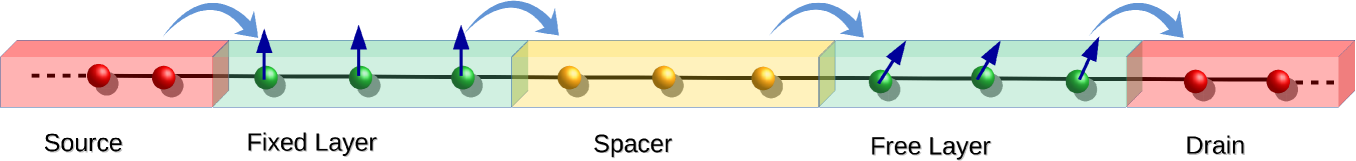
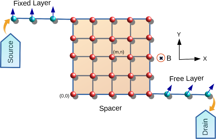
We substantiate our proposal with the junction set-up given in Fig. 1, where the NM layer plays the central role. One key idea is that we need to select the spacer in such a way that the bridging magnetic-non magnetic-magnetic (M-NM-M) system exhibits multiple energy bands and they are arranged, in energy scale, differently with the parallel (P) and anti-parallel (AP) configurations of the magnetic layers. Under this situation MR can be obtained by selectively choosing the Fermi energy of the system, and this is one of our primary requisites. The other pivotal requirement is that the MR can be tuned externally. Both these two conditions will be fulfilled with the help of an AAH spacer AAH1 ; AAH2 ; AAH3 ; AAH4 ; AAH5 ; AAH6 ; AAH7 , a quasicrystal, which has been a classic example of gaped systems. Quasicrystals are found to exhibit several non-trivial topological phenomena that are being considered as newly developed paradigms in the discipline of condensed matter physics. The diverse characteristic features of AAH models make them truly unique over the other quasicrystals, and several spectacular phenomena have already been revealed considering both the diagonal and/or off-diagonal versions through a reasonably large amount of recent theoretical and experimental works AAH1 ; AAH2 ; AAH3 ; AAH4 ; AAH5 ; AAH6 ; AAH7 . The AAH phases associated with the diagonal and off-diagonal parts, those are tuned externally and independently, regulate the energy band structure significantly, and thus, tunable physical properties are naturally expected.
To make the proposed model more realistic we include the effects of dephasing AAH7 ; Deph1 ; Deph2 ; Deph3 ; Deph4 . It is an important factor that can destroy the phase memory of charge carriers, and thus, it can affect the transport properties. Among many sources the most probable one is the electron-phonon (e-ph) interaction. Now inclusion of this effect has always been a challenging task, and although some prescriptions are available, most of them are based on density functional theory (DFT)
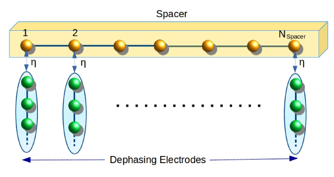
within a non-equilibrium Green’s function (NEGF) formalism which are too heavy to implement properly and also very time taking dft1 . But Büttiker came up with a simple and elegant idea to analyze the effect of dephasing dp1 ; dp2 ; dp3 , where virtual electrodes (voltage) are connected at each lattice sites of the bridging system (for illustration, see Fig. 2) those do not carry any net current, but they are responsible for randomizing the phases. As this is a classic way to include the effect of different dephasing mechanisms we incorporate it in our present analysis. The main motivation for the consideration of this effect is to test whether the phenomena studied here still persist even in presence of dephasing or not. If they persist, then we will have a suitable hint that the proposed model can be tested in laboratory under different realistic situations.
We define GMR as , where and correspond to net conductances for the parallel and anti-parallel spin configurations, respectively. Usually GMR is referred as . In this definition a situation may arise especially for the ballistic case, which can be understood from our forthcoming analysis, that drops almost to zero or in some cases it may vanish completely. Under this situation an infinite GMR will be obtained that we may call as absolute GMR, which cannot be shown in the graph. To avoid this, in our work, we mention GMR as , and with this definition no physics will be altered. If we get change in GMR, it means absolute GMR according to the other expression. In presence of environmental dephasing and other factors, though we get reasonable GMR, absolute GMR cannot be obtained which can also be understood from our upcoming discussion.
In order to calculate GMR, we need to determine conductance and we evaluate it from the spin dependent transmission probabilities, , following the Landauer conductance formula green1 , where . All these components, , are computed using the non-equilibrium Green’s function (NEGF) formalism, which is the most suitable and standard technique to study transport properties. In this formulation, an effective Green’s function is formed by incorporating the effects of contact electrodes through self-energy corrections and it can be written as green1 : , where and are the contact self-energies, and and are the tunnel Hamiltonians due to source (S) and drain (D). is the Hamiltonian of the bridging conductor which is a sum , where and are the Hamiltonians associated with the magnetic and non-magnetic parts, respectively. We describe all these Hamiltonians within a tight-binding (TB) framework. Using the above Green’s function we evaluate spin dependent transmission probabilities through the Fisher-Lee relation green2 , where ’s () are the coupling matrices.
The spin dependent scattering mechanism exists only in the magnetic layers, separated by a NM spacer, and considering this effect the TB Hamiltonian of the magnetic layer reads as ham1 ; ham2 ; mp1 , where , are the Fermionic operators, and and are the () diagonal matrices associated with site energy (, ) and nearest-neighbor hopping (NNH) integral () of up and down spin electrons. is the spin dependent scattering term where is the strength of magnetic moment at site and () is the Pauli spin vector with in diagonal representation. The orientation of any magnetic moment is described by the usual polar angle and azimuthal angle in spherical polar co-ordinate system. For the NM spacer a similar kind of TB Hamiltonian, apart from the term , is used. Now, in presence of AAH modulation, the site energy of the spacer becomes AAH5 , where is the strength of modulation and is a constant factor that can be a commensurate or an incommensurate one. For the incommensurate AAH model we choose as the golden mean i.e., ()/2. The other physical parameter in the site energy expression, the so-called AAH phase, plays an important role and it can be tuned externally with suitable set-up AAH2 ; AAH5 . We will critically examine its effect on GMR.
The TB Hamiltonians for the source and drain read as , where different terms correspond to the usual meanings. These electrodes are coupled to the bridging system via the coupling parameters and , respectively. We assume S and D as perfect, semi-infinite, one-dimensional and non-magnetic.
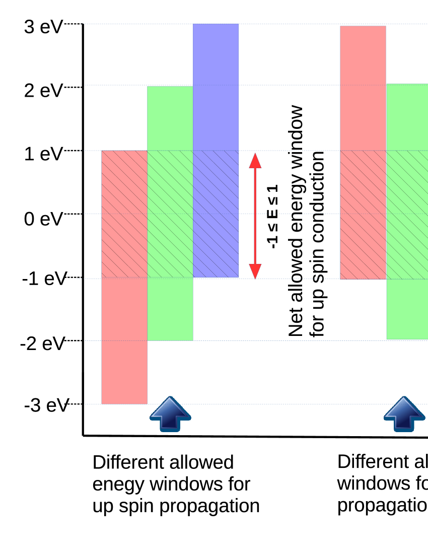
In order to include dephasing effect following the Büttiker prescription we need to couple virtual electrodes, similar to real electrodes, at each lattice site of the conductor (see Fig. 2). All these electrodes are parametrized identically with S and D, and they are non-magnetic. The coupling strength (also referred as the dephasing strength) between the spacer and the dephasing electrodes is described by the parameter . Now, to have the condition that these electrodes are not carrying any finite current, we have to adjust potentials () of the virtual electrodes accordingly, such that the voltage drop across each of these electrodes is perfectly zero. That is in principle possible with the application of a finite bias across the contact electrodes S and D i.e., (say) and . Under this situation, the effective spin dependent transmission probability is expressed as dp3 : .
Before analyzing the results let us mention the values of the physical parameters those are common throughout the calculations. The on-site energies for the perfect lattice sites are chosen as zero, and they are same for both up and down spin electrons. The NNH integral, , in S and D is fixed at , and the other NNH integrals along with contact-to-conductor coupling strength i.e., , and , are set at . As the dephasing strength is not common for all figures, we specify it in the appropriate places during our analysis. The strength of magnetic moments () and the azimuthal angle () are fixed at one and zero, respectively. The number of sites in the fixed and free magnetic layers are referred as and , and we set them at . On the other hand, for the NM spacer we specify the total number of atomic sites by , and unless specified otherwise, we set it at . All the energies are measured in unit of electron volt (eV).
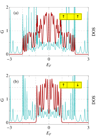
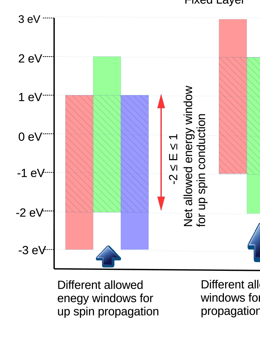
Now we explain our results. As already stated, our central focus is to achieve a high degree of GMR and its suitable tuning. Before describing the tuning mechanism, let us start to analyze how to get high GMR. The key concept of getting high GMR is that we need to achieve higher conductance for one configuration of the free layer, and most importantly much lower conductance in the other configuration. If this lower conductance drops exactly to zero, then change in MR will be obtained. This can be achieved considering the layered structure as illustrated in Fig. 3. For the parallel configuration, finite conductance is obtained within the range (red line of Fig. 3(a)), whereas spin transmission gets perfectly blocked for both up and down spin electrons within the ranges and in the anti-parallel configuration (red line of Fig. 3(b)). Thus, setting the Fermi energy anywhere within these two zones, viz, and , GMR will be noticed. The allowed and the forbidden zones of different spin electrons for the two different configurations of magnetic moments can be understood from the energy bar diagrams shown in Figs. 3(e) and (f). The electron can transmit through the junction only when a common energy channel is found. What we see is that, for the parallel configuration one can get finite transmission, due to up or down spin electron, in the range , among which is the overlap region for both the two spin electrons. This scenario is exactly reflected in the spectrum Fig. 3(a). When the magnetic moments of the free layer get flipped to make an anti-parallel configuration, the situation becomes more interesting. From the energy bar diagram Fig. 3(f) we can see that only within the range both the up and down spin electrons can propagate, while all other zones are blocked. This is the key advantage of a layered structure. More and more selective transmitting zones can be generated by combining more number of magnetic and NM spacers, which we check through our detailed calculations, and thus more controlled transmission will be obtained. Comparing the spectra given in Figs. 3(a) and (b) it is now clear that change in resistance can be possible by selectively choosing the Fermi energy.
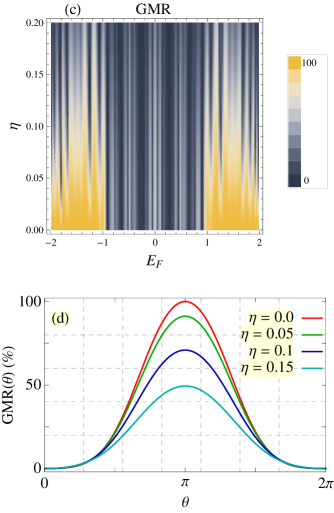
The effect of dephasing is quite interesting. From the simultaneous variation of GMR with and (Fig. 3(c)), we can see that for a reasonable dephasing strength a high degree of GMR is obtained. With increasing it gradually decreases, and eventually drops to zero for large enough strength, as expected.
Now, to examine the role of on GMR, in Fig. 3(d) we plot GMR as a function of (which we call as GMR()) at some typical values of dephasing strength. For each , the change in resistance increases with , and it reaches to a maximum when all the magnetic moments of the free layer are completely aligned in the opposite direction with respect to the fixed layer yielding maximum scattering. This phenomenon leads to an important message along with the magnetoresistance that selective spin dependent electron transport can be achieved by changing the orientation of magnetic moments uniformly in one segment of the junction.
The results analyzed so far are worked out considering a perfect spacer (). Now, keeping in mind the possible engineering of GMR, we replace the perfect
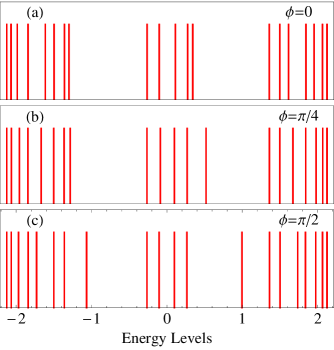
spacer by the AAH one. The speciality of the AAH spacer is that it exhibits gaped spectrum, as clearly seen from Fig. 4 where the energy levels are plotted for a -site incommensurate AAH chain at three typical values of . In addition to that, the possible tuning of energy spectrum
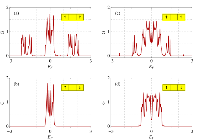
is also clearly reflected, which is another key advantage of AAH lattices compared to other conventional uncorrelated and correlated disordered ones. Because of the gaped spectrum exhibited by the AAH spacer, several energy zones are expected where finite transmission is available from one configuration (parallel), while almost zero contribution is obtained for the other configuration (anti-parallel). This is exactly reflected from the spectra given in Figs. 5(a) and (b), where the conductance is shown for an incommensurate AAH spacer. The zero contribution in conductance for the anti-parallel arrangement is due to the non-availability of common spin channel, as clearly discussed earlier in the case of perfect spacer. Multiple energy windows are available where conductance drops exactly zero in the anti-parallel configuration resulting a change in MR. Several such energy windows cannot be observed in the case of a perfect spacer. For the sake of completeness, in Figs. 5(c) and (d) we present the results of a commensurate AAH spacer, and comparing the spectra given in Fig. 5 we can clearly emphasize that the incommensurate AAH spacer is superior than the commensurate one. Here we would like to note that, for commensurate the system becomes a perfect one which exhibits always extended energy eigenstates. Whereas, for the incommensurate the system becomes a correlated disordered one which thus exhibits non-trivial energy spectrum rather than a commensurate one. Because of this fact, interesting behavior in transport phenomena is naturally expected for incommensurate AAH system.
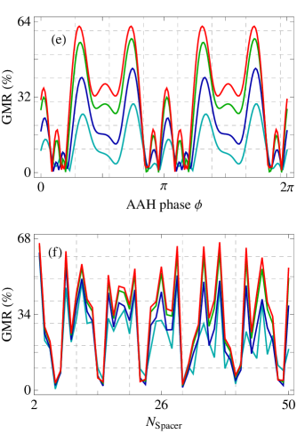
From the spectra shown in Fig. 4 it is now clear that AAH phase has a critical role in energy band engineering, which thus definitely be reflected in GMR effect. Now we analyze it clearly. In the energy regions where finite conductance is obtained for one configuration and the conductance becomes zero for the other configuration, always GMR will be obtained, and hence there will be no meaning to examine the effect of AAH phase in those energy zones. Therefore, we select in such a way where conductance is finite for both the two configurations of the magnetic layers. Here we set . From the results given in Fig. 5(e) we find that a reasonably large change in GMR is obtained by tuning the phase factor for each dephasing strength which leads to an important conclusion that one can selectively choose the phase to achieve higher GMR, and most importantly, it can be performed externally AAH2 ; AAH5 . In this context it is relevant to note that few other proposals have also been made in different set-ups for possible tuning of MR externally kmr1 ; kmr2 ; kmradd1 . For instance, considering a graphene heterostructure Bala Kumar et al. kmr1 have shown that a large MR can be achieved upon the application of magnetic field, employing the specific properties of wave functions in the field and zero-field cases. On the other hand, in another work by Bala Kumar and co-workers kmr2 it has been established that band engineering can be possible in graphene nanoribbon by applying external magnetic field which leads to a large change in MR. With these proposals we get a clear confidence for implementing a new prescription of externally controlled mechanism of MR. Our work, thus definitely a new addition along this line.
Finally, to test how the results are sensitive to the size of the AAH spacer, in Fig. 5(f) we plot GMR by varying the length of the spacer considering and . It exhibits pronounced oscillations providing almost constant amplitude with , which gives us a hint of choosing the dimension of the spacer for better performance.
From the results studied here we see that both for the ordered and AAH spacers, though GMR gets reduced with dephasing strength , high degree of GMR can still be observed for a reasonably large . This is one way (means the inclusion of dephasing) to include the environmental effects/disturbances, as put forward by Büttiker and many other groups. At the same time another few factors are also there that may affect the GMR. For instance, bulk disorder and/or edge vacancies, depending on the specific geometry of the conducting junction. It is true that disorder modifies the transport properties kmr3 ; yao ; gangu , but as GMR
is the ratio between two conductances, significant change in GMR will not be noticed even for moderate disorder strength, which can also be confirmed from our results considering the AAH spacer (AAH model is called as the correlated disordered one). For strong enough disorder, when the states are almost localized, naturally we cannot expect any such phenomena.
Now, considering the unique and diverse characteristic features of AAH lattices, one proposition may come to our mind that instead of using an AAH spacer between two magnetic layers can we think about a GMR set-up where the effect of AAH potential is directly implemented into the magnetic layers, removing the spacer region. Of course the opportunity of energy band engineering will be still there by changing the AAH phase, but in the absence of NM spacer, two magnetic layers will then interact with each other because of the magnetic exchange interaction among them, which essentially affects the magnetic layers. To avoid this magnetic interaction, the inclusion of a NM layer is highly recommended, as used in other GMR studies.
For experimental realization of our proposed model, we can think about a set-up given in Fig. 6 where two magnetic layers are separated by a 2D lattice subjected to a transverse magnetic field , the so-called quantum Hall system. It is well-known that a 2D Hall system maps exactly to an effective 1D chain where the site energy gets modulated with the factor . Thus, selectively tuning the magnetic field one can design a spacer in the form of AAH chain, and in principle, can examine the results studied here.
In conclusion, we have established a new proposal to achieve better performance in magnetorestive effect exploiting the unique features of correlated disordered lattice, that has not been reported so far in literature to the best of our knowledge. The persistence of the results even in presence of large dephasing strength gives us a confidence that the proposal can be substantiated experimentally with suitable set-up. What comes out from the entire analysis is that the essential mechanism of magnetoresistance is hidden within the non-trivial characteristics of different spacers, and here we have shown one example along this direction considering an AAH system. We also get a strong confidence about our claim following one recent work done by Wang et al. wang . Considering a bottom-pinned perpendicular anisotropy-based magnetic tunnel junction (p-MTJ, stacked with Tungsten (W) layers and MgO/CoFeB interfaces, they have shown that a large magnetoresistance can be achieved, circumventing Tantalum (Ta) as the spacer as was used previously in other p-MTJ films. Thus, undoubtedly the spacer has the most significant role in magnetoresistive study. Although several propositions have been put forward, still more investigations are required for better performance.
SKM would like to thank the financial support of DST-SERB, India under Grant No. EMR/2017/000504.
References
- (1) M. N. Baibich et al., Phys. Rev. Lett. 61, 2472 (1988).
- (2) G. Binash, P. Grünberg, F. Saurenbach, and W. Zinn, Phys. Rev. B 39, 4828 (1989).
- (3) P. Grünberg, R. Schreiber, Y. Pang, M. B. Brodsky, and H. Sowers, Phys. Rev. Lett. 57, 2442 (1986).
- (4) S. S. P. Parkin, N. More, and K. P. Roche, Phys. Rev. Lett. 64, 2304 (1990).
- (5) A. Berkowitz et al., Phys. Rev. Lett. 68, 3745 (1992).
- (6) J. Mino et al., J. Electron. Mater. 45, 2401 (2016).
- (7) B. Dieny, V. S. Speriosu, S. S. P. Parkin, B. A. Gurney, D. R. Wilhoit, and D. Mauri, Phys. Rev. B 43, 1297 (1991).
- (8) L. Liu et al., AIP Advances 6, 035206 (2016).
- (9) R. R. Katti, D. Zou, D. Reed, and H. Kaakani, IEEE Trans. Magn. 39, 2848 (2003).
- (10) A. P. Ramirez, J. Phys.: Condens. Matter 9, 8171 (1997).
- (11) Y. Tokura, Ed., Colossal Magnetoresistive Oxides, Gordon and Breach, New York (2000).
- (12) M. B. Salamon and M. Jaime, Rev. Mod. Phys. 73, 583 (2001).
- (13) R. Ranchal et al., Nanotechnology 13, 392 (2002).
- (14) M. Djamal and Ramli, Procedia Eng. 32, 60 (2012),
- (15) P. Bruno, Phys. Rev. B 52, 411 (1995).
- (16) J. Mathon et al., Phys. Rev. Lett. 74, 3696 (1995).
- (17) J. Mathon et al., Phys. Rev B 56, 11797 (1997).
- (18) S. Aubry and G. André, Ann. Isr. Phys. Soc. 3, 133 (1980).
- (19) S. Ganeshan, K. Sun, and S. Das Sharma, Phys. Rev. Lett. 110, 180403 (2013).
- (20) M. Patra and S. K. Maiti, Sci. Rep. 7, 14313 (2017).
- (21) Y. Lahini et al., Phys. Rev. Lett. 103, 013901 (2009).
- (22) Y. E. Kraus et al., Phys. Rev. Lett. 109, 106402 (2012).
- (23) S. K. Maiti, S. Sil, and A. Chakrabarti, Ann. Phys. (N. Y.) 382, 150 (2017).
- (24) M. Patra and S. K. Maiti, J. Magn. Magn. Mater. 484, 408 (2019).
- (25) D. Nozaki, Y. Girard, and K. Yoshizawa, J. Phys. Chem. C 112, 17408 (2008).
- (26) D. Nozaki, C. G. da Rocha, H. M. Pastawski, and G. Cuniberti, Phys. Rev. B 85, 155327 (2012).
- (27) C. J. Cattena, R. A. Bustos-Marun, and H. M. Pastawski, Phys. Rev. B 82, 144201 (2010).
- (28) M. Dey, S. K. Maiti, and S. N. Karmakar, Org. Electron. 12, 1017 (2011).
- (29) N. Sergueev, A. A. Demkov, and H. Guo, Phys. Rev. B. 75, 233418 (2007).
- (30) M. Büttiker, Phys. Rev. Lett. 57, 1761 (1986).
- (31) M. Büttiker, IBM J. Res. Dev. 32, 63 (1988).
- (32) T.-R. Pan, A.-M. Guo, and Q.-F. Sun, Phys. Rev. B 92, 115418 (2015).
- (33) S. Datta, Electronic Transport in Mesoscopic Systems, Cambridge University Press, Cambridge (1997).
- (34) D. S. Fisher and P. A. Lee, Phys. Rev. B 23, 6851 (1981).
- (35) A. A. Shokri and M. Mardaani, Solid State Commun. 137, 53 (2006).
- (36) M. Dey, S. K. Maiti, and S. N. Karmakar, Eur. Phys. J. B 80, 105 (2011).
- (37) M. Patra and S. K. Maiti, Europhys. Lett. 121, 38004 (2018).
- (38) S. Bala Kumar, M. B. A. Jalil, and S. G. Tan, Appl. Phys. Lett. 101, 183111 (2012).
- (39) S. Bala Kumar, M. B. A. Jalil, S. G. Tan, and G. Liang, J. Appl. Phys. 108, 033709 (2010).
- (40) Z. Y. Leong, S. G. Tan, M. B. A. Jalil, S. Bala Kumar, and G. C. Han, J. Magn. Magn. Mater. 310, e635 (2007).
- (41) S. Bala Kumar, M. B. A. Jalil, S. G. Tan, and G. Liang, J. Phys.: Condens. Matter 22, 375303 (2010).
- (42) Y. X. Yao, C. Z. Wang, G. P. Zhang, M. Ji, and K. M. Ho., J. Phys.: Condens. Matter 21, 235501 (2009).
- (43) S. Ganguly, S. Basu, and S. K. Maiti, Europhys. Lett. 124, 17005 (2018).
- (44) M. Wang et al., Nat. Commun. 9, 671 (2018).