Co-existence of spin semi-metallic and Weyl semi-metallic behavior in FeRhCrGe
Abstract
In this letter, we report the discovery of a new class of spintronic materials, namely spin semi-metals (SSM), employing both theoretical and experimental tools. The band structure of this class of materials is such that one of the spin bands resembles that of a semi-metal, while the other is similar to that of an insulator/semiconductor. This report is the experimental verification of the first SSM, FeRhCrGe, a quaternary Heusler alloy with a magnetic moment 3 and a Curie temperature of 550 K. The measurement below 300 K shows nearly temperature independent conductivity and a relatively moderate Hall effect. SSM behavior for FeRhCrGe is also confirmed by rigorous first principles calculations. Band structure calculations also reveal that the spin up (semi metallic) band has combined features of type II Weyl and nodal line semimetal. As such, this study opens up the possibility of a new class of material with combined spintronic and topological properties, which is important both from fundamental and applied point of view.
pacs:
85.75.-d, 75.47.Np, 75.76.+j, 76.80.+yIntroduction: Recent developments in magnetic Heusler alloys, such as the discovery of half metallic ferromagnets (HMF) have fuelled the area of spintronics research considerably.de Groot et al. (1983); Katsnelson et al. (2008); Felser et al. (2007); Felser and Fecher (2013); Ching-yao et al. (2013) One of the spin bands is metallic while the other is either semiconducting or insulating in this class of materials. Later, spin gapless semiconductors (SGS)Wang (2008) were discovered which gained prominence over the half metals due to their unique properties. Magnetic semiconductorsLi et al. (2012) with unequal band gaps constitute another class of spintronic materials that produce high spin polarized charge carriers at elevated temperatures. Fully compensated ferrimagnetVenkateswara et al. (2018) is another unique class. In this letter, we discovered a new interesting class of materials, which we term as spin semi-metals (SSM). One of the main motives of this paper is to highlight the discovery of SSM and its importance and applications in the field of spintronics. We demonstrate the existence of necessary features of SSM in a realistic material, FeRhCrGe. Furthermore, the spin up band of this material is also found to acquire a combined feature of type II WeylXu et al. (2015); Huang et al. (2015) and nodal lineFang et al. (2015); Bian et al. (2016) semi-metal.
One of the necessary conditions for a spintronic material is to possess integer magnetic moment (), for which the density of states (DoS) should be zero for at least one spin bands.Venkatesan (2007) This leads to six possible classes of materials namely (i) conventional semiconductors, (ii) simple gapless semiconductors, (iii) magnetic semiconductors, (iv) half metals, (v) SGS and (vi) SSM. Schematic band structures of all these are shown in Fig S1 of supplementary material (SM).sup The first two classes do not produce any spin polarized carriers in their electrical conduction due to symmetric spin up and down DoS. Spin semimetals are expected to be potential materials as they produce both spin polarized electrons and holes, similar to SGS materials. The identification of many HMF and SGS materials from the Heusler family has resulted in a renewed interest in the field of spintronics due to their interesting properties such as high Curie temperature (TC), structural stability and compatibility to grow thin films.Felser and Hirohata (2015); Bainsla and Suresh (2016) In this context, we would like to highlight an interesting observation that, only a certain discrete set of lattice parameter of Heusler alloys gives rise to the above mentioned six classes of materials. This critical separation is found to be nearly 0.123 Å. Taking the lattice parameter of Co2MnSiRaphael et al. (2002) (5.65 Å) as one of the those allowed values, the lattice parameters corresponding to other Heusler alloys are tabulated in Table S1 of SM.sup
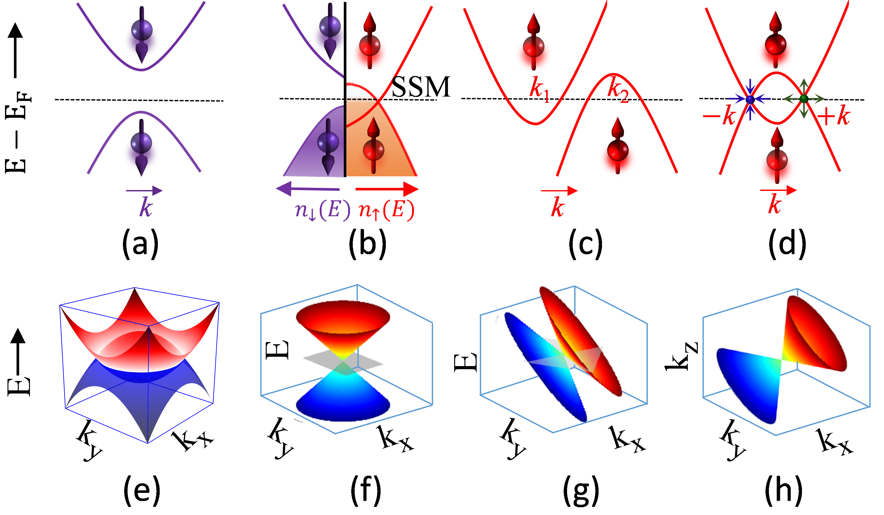
Spin semimetals are a unique class of spintronic materials, in which one of the spin bands is semi-metallic while the other is either insulating or semiconducting. The spin semimetallic band consists of partial overlap of two or more different types of valence and conduction bands. It causes a large DoS at the Fermi level (E) in the spin semimetallic band. However, they show negative temperature coefficient in their electrical resistivity, which is due to the presence of electron and hole pockets at E. Figure 1(b) shows a schematic spin resolved DoS for SSM, in which spin down DoS is gapped (bands shown in Fig.1(a)), while the spin up DoS is due to the partial overlap of valence and conduction bands with the possibilities of indirect (Fig.1(c)) or direct (Fig.1(d)) overlapping. Direct overlap often causes doubly degenerate band crossing at and points, which are analogous to Weyl points in 1D. Weyl nodes or points are the points in the 3D Brillouin zone (BZ) which possess cone-like energy spectrum.Wan et al. (2011) It is well known that the Weyl nodes are protected in magnetic systems due to the lifting of spin degeneracy at the nodes.Wan et al. (2011); Wang et al. (2016) These nodes act as sources and sinks of Berry flux. In fact, the 1D Weyl like nodes can evolve as either (i) nodal line or (ii) type I or type II Weyl points in the 3D band structure. 2D projected band structure for nodal line, type I and type II Weyl points are shown in Fig. 1(e)-(g). It has been reported that the Weyl nodes can occur at points other than high symmetry -path unlike nodal line semimetals.Wan et al. (2011); Yang et al. (2018) Type I Weyl points cause point-like Fermi surface (FS) and hence difficult to identify. However, 2D band structure of tilted Dirac cone causes the crossed Fermi lines (see Fig.1(g)) centred at Weyl node. Soluyanov et al. (2015) These crossed Fermi lines evolve into Dirac cone centred at type II Weyl point in the 3D band structure (see Fig.1(h)). Hence, the presence of type II Weyl points can be easily identified by locating the position of Dirac cone FS in the 3d BZ. To be a Weyl point, each cone must belong to different bands.Zubkov and Lewkowicz (2018)
In general, the nature of overlapping bands near E can be different e.g. overlap of either (i) flat valence and sharp conduction bands or (ii) sharp valence and flat conduction bands, or (iii) flat valence and flat conduction bands with E spectrum different from parabolic nature. Different possibilities of E spectrum near E were discussed by X. L. WangWang (2008) for SGS. The same scenario can be expected in SSM as well. However, unlike SGS materials in which spin gapless nature is extremely sensitive to the disorder, pressure and impurities, SSM are expected to be less sensitive yet giving a high spin polarization due to the presence of large DoS at . With the semimetallic nature of one spin band in SSM, this also leads to the possibility of hosting Weyl fermions in the semimetallic band, in addition to the presence of standard spin polarized electrons and holes. As such, SSM materials having signatures of Weyl nodes lead to a completely new era for spintronic materials.
In this letter, we report the first spin semimetallic material, namely quaternary Heusler alloy FeRhCrGe, based on the confirmation from both experimental and theoretical investigations. We also confirm that this alloy shows type II Weyl nodes in the semimetallic band, resulting in the realization of Weyl fermions.Shi et al. (2018) Finally, with the help of molecular energy level diagram, we propose that, 27 valence electron quaternary alloys can, in general, be a promising playground to find potential SSM materials.
FeRhCrGe belongs to a quaternary Heusler alloy (XXYZ) with space group Fm. The structure can be seen as 4 interpenetrating fcc sublattices with Wyckoff positions 4a, 4b, 4c and 4d. The possible non-degenerate configurations for a general XX′YZ quaternary alloy (fixing Z-atom at 4a-site) are (I) X at 4c, X′ at 4d and Y at 4b site, (II) X at 4b, X′ at 4d and Y at 4c site, (III) X at 4c, X′ at 4b and Y at 4d site. Configuration I turns out to be energetically the most stable one.
I Experimental results
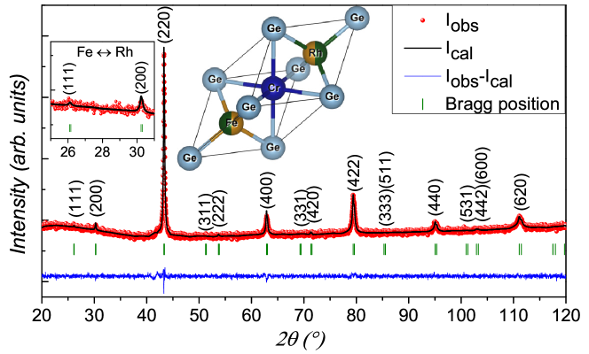
Crystal Structure : Room temperature X-ray diffraction (XRD) pattern along with the Rietveld refinement for the configuration I with 50% anti-site disorder between tetrahedral site atoms Fe and Rh is shown in Fig. 2. A more detailed analysis of XRD pattern is presented in SM.sup Due to the presence of antisite disorder, we conclude that FeRhCrGe crystallizes in L21 structure (crystal structure shown in the inset of Fig. 2).
Magnetization : According to the Slater-Pauling (SP) rule,(Graf et al., 2011) the saturation magnetization ( in units of ) in the present case is given by , where is the total number of valence electrons of the Heusler alloy. It predicts 3 for FeRhCrGe.
Magnetization data (M vs. H and M vs. T) indicating ferromagnetic behaviour of FeRhCrGe is shown in Fig. S3 of SM.sup at 3 K is nearly 2.9 , which agrees fairly well with SP rule. T is found to be 550 K.
Transport properties : Figure 3(a) shows resistivity () vs. T at different H for FeRhCrGe. Negative temperature coefficient of indicates the possibility of either a semiconductor or a semimetal. However, the absence of exponential dependence precludes the gapped semiconducting nature. Therefore, it could either be a simple gapless semiconductor, SGS or a semimetal. To further understand the transport behavior, conductivity data is fitted with the modified two-carrier modelKittel (2007); Jamer et al. (2017)
| (1) |
where, are the carrier concentrations of electrons, holes with mobilities . are the energy gaps. A fit to in the zero field, high T-region is shown in Fig. 3(b). The energy gaps obtained are 53.4 and 0.3 meV. Using the Hall data (explained below), the lower band gap is assigned to the holes.
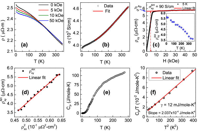
Hall resistivity () vs. H is shown in Fig. 3(c) which is typical of a ferromagnetic material. In such materials, is contributed by both ordinary and anomalous Hall resistivities i.e., , where () is the coefficient of ordinary (anomalous) Hall resistivity. The Hall conductivity () is estimated using the relation,
The estimated anomalous Hall conductivity 90 S/cm at 5 K. The carrier concentration was estimated from the ordinary Hall coefficient () which in turn is extracted from the linear fit of high field data (above 15 kOe). The positive value of the ordinary Hall coefficient hints to the fact that the holes are the majority charge carriers. The concentration of hole carriers is found to be . Anomalous Hall resistivity () is estimated from the y-intercept of the extrapolated high field linear fit. The inset of Fig. 3(c) shows the T-dependence of , which follows a similar trend as that of zero-field resistivity. In order to obtain the intrinsic and extrinsic anomalous Hall conductivities, is scaled to (see Fig. 3(d)) using the empirical formula,Tian et al. (2009) . The fitting gives and , where and are related to extrinsic and intrinsic contributions, respectively. The negative value of indicates that the extrinsic contribution is opposite to the Karplus-Luttinger termKarplus and Luttinger (1954) (intrinsic contribution). The intrinsic anomalous Hall conductivity is .Tian et al. (2009) We have also simulated the intrinsic anomalous Hall conductivity using Berry curvature calculations (see Sec. II). The measured is nearly one fourth of the theoretically estimated value. Such a low value could be due to the presence of both types of charge carriers and degenerate flat bands at E, in which some of the heavy carriers get trapped and easily recombine with the opposite carriers before they reach the edges of the sample.
Specific heat : Figure 3(e) shows the specific heat (C) vs. T. The electronic contribution to C in simple gapless semiconductor or SGS is quite small compared to that of metals or semi-metals due to vanishing DoS at E. Figure 3(f) shows the vs. T2 along with the linear fit. Using the free electron gas model, the DoS at E can be estimated fromTseng et al. (2017) , where is the Sommerfeld constant. The value of (12 mJ/mole-K2), obtained from the fit, yields states/eV-f.u., which is in good agreement with the simulated results (see Sec. II). Hence, it is quite evident that FeRhCrGe is neither a simple gapless semiconductor nor a SGS; instead it is very likely to be a spin semimetal.
II Theoretical Results
Computational details are given in Sec. C of SM.sup Within ab-initio framework, all the three non degenerate configurations were fully relaxed with parallel spin moments on each magnetic ions and the results are shown in Table II of SM.sup Configuration I turns out to be the ground state with ferromagnetic ordering. This configuration is consistent with the empirical rule based on electronegativities.(Graf et al., 2011; Enamullah et al., 2015) Theoretically optimized lattice parameter ( Å) agrees well with experimental value. The calculated net magnetization (/f.u.) is in good agreement with the value obtained from SP rule, as well as that of experiment (2.90 ) at 3 K.
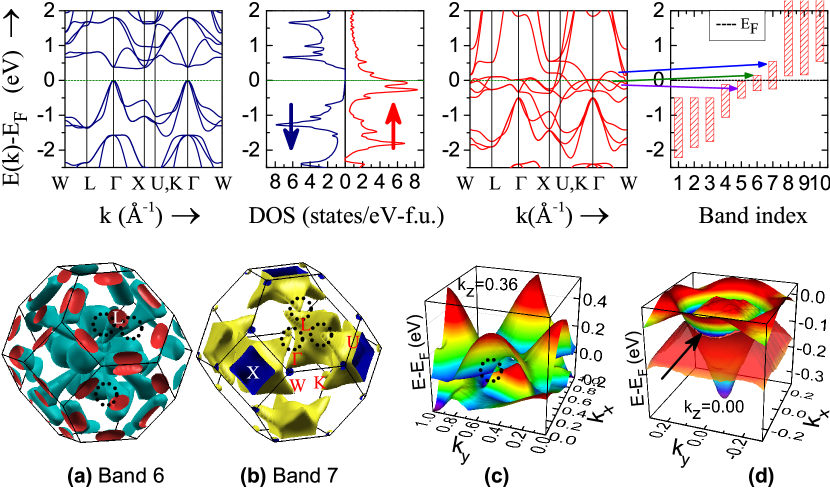
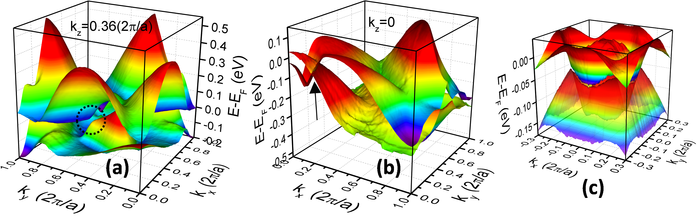
Figure 4 (top) shows the spin polarized band structure and DoS for the ground state configuration at the relaxed lattice parameter. The extreme right panel (top) shows the band width of various spin up bands contributing to the DOS near E. Notably, the large DoS at E for spin up channel mainly arises from flat bands. Combination of bands 6 and 7 resembles that of a typical semi-metal. Figure 4(a,b) (bottom) shows the FS arising out of bands 6 and 7. As discussed earlier, type II Weyl nodes cause the Dirac cone FS at that point. The location of these points is indicated by dotted circles in Fig. 4(a,b). Figure 4(c) shows the E spectrum at plane. The positions of tilted Dirac cones were found at (0.36,0.59,0.36) and (0.59,0.36,0.36). The other point exists at (0.64,0.64,0.41). There are a total of 24 type II Weyl points in the entire BZ (3 around each of 8 -points). A similar scenario was also observed by Wan et. al. in Y2Ir2O7,Wan et al. (2011) having type I Weyl points. Weyl points are the sources of ’Berry flux’ in the momentum space but the net flux due to all Weyl points in the BZ vanishes (due to opposite chirality).Wan et al. (2011) To understand the pattern of Berry curvature around these points, non-collinear spin calculations with spin orbit coupling (SOC) were also performed.
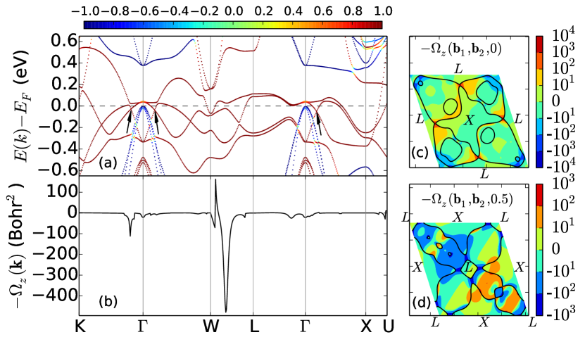
With inclusion of SOC, magnetic ground state of configuration I turns out to be collinear with total moment . The moments on individual magnetic ions are nearly same as those obtained from collinear spin calculations. Figure 5(a) shows the SOC band structure, with th colour profile indicating the value of projected spin on the magnetization direction. Apparently, spin character of the bands near E is pure, which is crucial to retain high spin polarization and also spin semi-metallic nature. Figure 5(b) shows the z-component of the simulated Berry curvature along the high symmetry k-points while Fig. 5(c) and (d) shows on and planes respectively. Notice the change of sign of Berry flux around L point, as we move from to planes. Magnitude of flux, however, is not same which needs to be equal and opposite to be a Weyl point.Wan et al. (2011) This indicates the deviation from a tilted Dirac cone, with the onset of a gap arising out of SOC effect. This is precisely shown in Fig. 6(a). The band (having spin up character) lying just below E ( meV), retains topological character. Notice from Fig. 5(a), that the degeneracy of these bands at certain points along high symmetry lines is not lifted, i.e., (i) one set of points along , and indicating the possibility of nodal line semi-metal with energies lying between 28 to 50 meV below E and (ii) few other nodal and Weyl points below eV. Figure 6(b) shows the presence of nodal line in the spin up band. A zoomed view around the nodal point is shown in Fig. 6(c). Very large Berry flux is seen at points (1,0.5,0.1), which are close to the high symmetry point . E has Dirac cone like behavior at these points. The intrinsic anomalous Hall conductivity is obtained by integrating over the entire BZ,Yao et al. (2004) i.e., , which turns out to be -495 . Obviously, this large value is due to the mismatch of the magnitude of Berry flux at the locations, as discussed earlier.
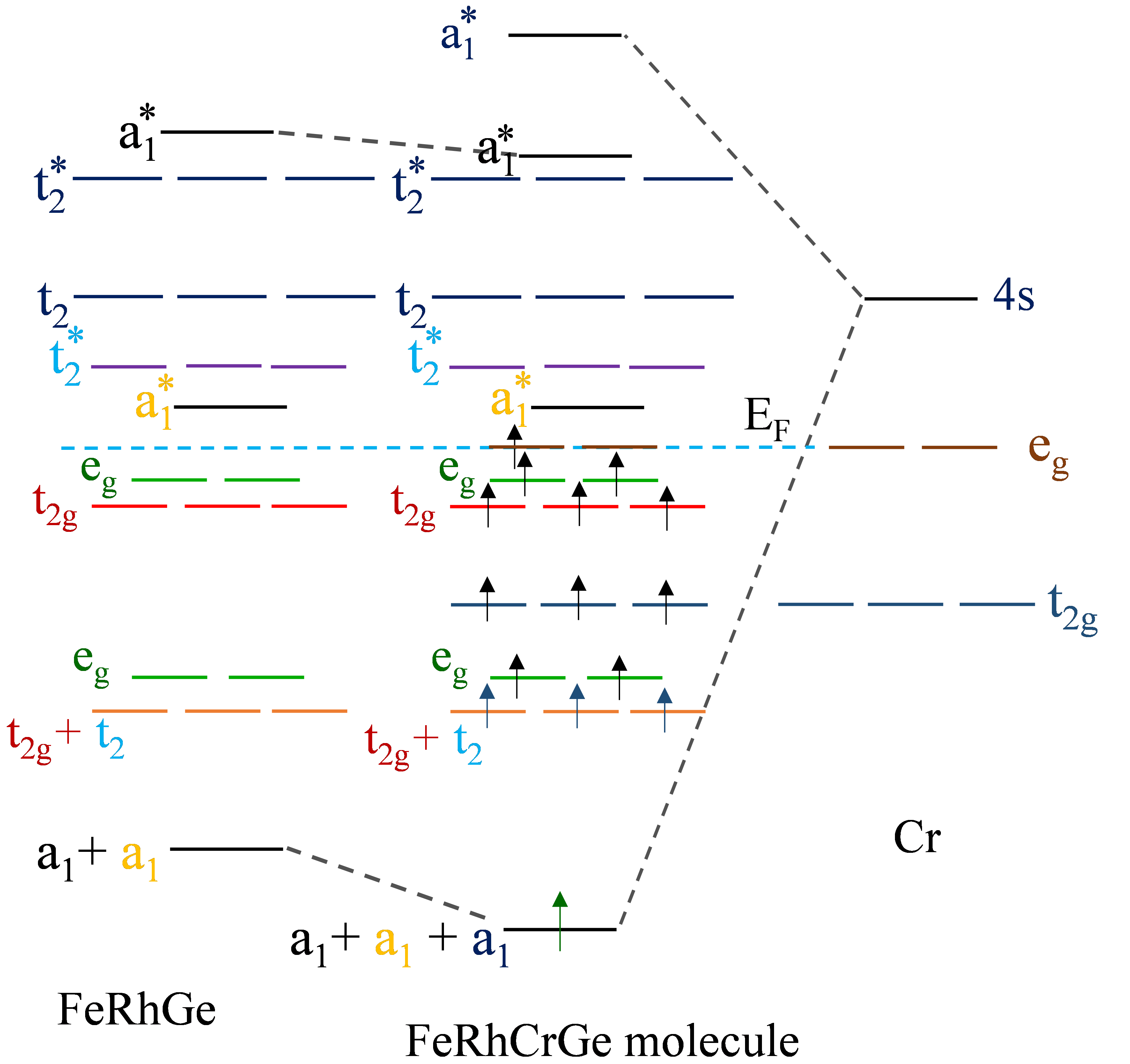
In the following, we explain the formation of unique band structure of FeRhCrGe using the molecular energy level diagram. Energy diagram at the molecular level is often quite informative in predicting the nature of bonding and transport. Such diagrams can be extracted from the orbital projected states at the -point. Orbital decomposed atom-projected states for the spin up and down channels for FeRhCrGe are shown in Fig. S6 and S7 of SM.sup The corresponding molecular level diagrams for various sub-molecules are shown in Fig. S8, S9 and S10.sup Figure 7 shows a schematic view of this diagram for spin up electrons. The energy levels are aligned as , , , , , , etc. for both spin bands. Here a1, a, t2 and t are the bonding and anti-bonding orbitals having s and p characters respectively. represents the mixed character of triply degenerate & orbitals. energy levels are filled in spin down channel and E lies in between anti-bonding levels of of FeRh submolecule, whereas it lies at the degenerate level of octahedral site atoms in spin up channel (see Fig. 7). These orbitals at EF are well localized in energy and are partially filled. These partially filled orbitals are responsible for creating electron and hole pockets in bulk FeRhCrGe, thereby bringing unique spin semi-metallic property.
Conclusion : In summary, we have discovered a new class of spintronic materials, termed as spin semimetals. Using detailed experimental and theoretical investigations, we show that FeRhCrGe is a spin semimetal with unique properties. Furthermore, careful band structure calculations show that this alloy acquire additional features of type II Weyl semimetal and nodal line semi-metal located close to Fermi level for the spin up band. In conclusion, we confirm the co-existence of spin semimetallic and Weyl semimetallic behavior in FeRhCrGe. This makes it the first candidate material in this new class which is interesting both from the fundamental understanding as well as applied perspective.
Acknowledgments :YV and SSS acknowledge the financial support provided by IIT Bombay. YV acknowledges the help of Mr. Akhilesh Kumar Patel and Miss Deepika Rani in the analysis of data. AA acknowledges National Center for Photovoltaic Research and Education (NCPRE), IIT Bombay for possible funding to support this research.
References
- de Groot et al. (1983) R. A. de Groot, F. M. Mueller, P. G. v. Engen, and K. H. J. Buschow, Phys. Rev. Lett. 50, 2024 (1983).
- Katsnelson et al. (2008) M. I. Katsnelson, V. Y. Irkhin, L. Chioncel, A. I. Lichtenstein, and R. A. de Groot, Rev. Mod. Phys. 80, 315 (2008).
- Felser et al. (2007) C. Felser, G. Fecher, and B. Balke, Angewandte Chemie International Edition 46, 668 (2007).
- Felser and Fecher (2013) C. Felser and G. Fecher, Spintronics: From Materials to Devices (Springer Netherlands, 2013).
- Ching-yao et al. (2013) F. Ching-yao, P. E, and Y. H, Half-metallic Materials And Their Properties, Materials For Engineering (World Scientific Publishing Company, 2013).
- Wang (2008) X. L. Wang, Phys. Rev. Lett. 100, 156404 (2008).
- Li et al. (2012) X. Li, X. Wu, Z. Li, J. Yang, and J. G. Hou, Nanoscale 4, 5680 (2012).
- Venkateswara et al. (2018) Y. Venkateswara, S. Gupta, S. S. Samatham, M. R. Varma, Enamullah, K. G. Suresh, and A. Alam, Phys. Rev. B 97, 054407 (2018).
- Xu et al. (2015) S.-Y. Xu, I. Belopolski, N. Alidoust, M. Neupane, G. Bian, C. Zhang, R. Sankar, G. Chang, Z. Yuan, C.-C. Lee, S.-M. Huang, H. Zheng, J. Ma, D. S. Sanchez, B. Wang, A. Bansil, F. Chou, P. P. Shibayev, H. Lin, S. Jia, and M. Z. Hasan, Science 349, 613 (2015).
- Huang et al. (2015) X. Huang, L. Zhao, Y. Long, P. Wang, D. Chen, Z. Yang, H. Liang, M. Xue, H. Weng, Z. Fang, X. Dai, and G. Chen, Phys. Rev. X 5, 031023 (2015).
- Fang et al. (2015) C. Fang, Y. Chen, H.-Y. Kee, and L. Fu, Phys. Rev. B 92, 081201 (2015).
- Bian et al. (2016) G. Bian, T.-R. Chang, R. Sankar, S.-Y. Xu, H. Zheng, T. Neupert, C.-K. Chiu, S.-M. Huang, G. Chang, I. Belopolski, D. S. Sanchez, M. Neupane, N. Alidoust, C. Liu, B. Wang, C.-C. Lee, H.-T. Jeng, C. Zhang, Z. Yuan, S. Jia, A. Bansil, F. Chou, H. Lin, and M. Z. Hasan, Nature Communications 7, 10556 EP (2016), article.
- Venkatesan (2007) M. Venkatesan, “Half-metals,” in Handbook of Magnetism and Advanced Magnetic Materials, Handbook of Magnetism and Advanced Magnetic Materials No. v. 4, edited by H. Kronmüller and S. Parkin (Wiley, 2007) pp. 2069–2070.
- (14) See Supplementary Material at [URL] for more details .
- Felser and Hirohata (2015) C. Felser and A. Hirohata, Heusler Alloys: Properties, Growth, Applications, Springer Series in Materials Science (Springer International Publishing, 2015).
- Bainsla and Suresh (2016) L. Bainsla and K. G. Suresh, Applied Physics Reviews 3, 031101 (2016).
- Raphael et al. (2002) M. P. Raphael, B. Ravel, Q. Huang, M. A. Willard, S. F. Cheng, B. N. Das, R. M. Stroud, K. M. Bussmann, J. H. Claassen, and V. G. Harris, Phys. Rev. B 66, 104429 (2002).
- Wan et al. (2011) X. Wan, A. M. Turner, A. Vishwanath, and S. Y. Savrasov, Phys. Rev. B 83, 205101 (2011).
- Wang et al. (2016) Z. Wang, M. G. Vergniory, S. Kushwaha, M. Hirschberger, E. V. Chulkov, A. Ernst, N. P. Ong, R. J. Cava, and B. A. Bernevig, Phys. Rev. Lett. 117, 236401 (2016).
- Yang et al. (2018) S.-Y. Yang, H. Yang, E. Derunova, S. S. P. Parkin, B. Yan, and M. N. Ali, Advances in Physics: X 3, 1414631 (2018).
- Soluyanov et al. (2015) A. A. Soluyanov, D. Gresch, Z. Wang, Q. Wu, M. Troyer, X. Dai, and B. A. Bernevig, Nature 527, 495 EP (2015).
- Zubkov and Lewkowicz (2018) M. Zubkov and M. Lewkowicz, Annals of Physics 399, 26 (2018).
- Shi et al. (2018) W. Shi, L. Muechler, K. Manna, Y. Zhang, K. Koepernik, R. Car, J. van den Brink, C. Felser, and Y. Sun, Phys. Rev. B 97, 060406 (2018).
- Graf et al. (2011) T. Graf, C. Felser, and S. S. Parkin, Progress in Solid State Chemistry 39, 1 (2011).
- Kittel (2007) C. Kittel, “Introduction to solid state physics, 7tth ed.” (Wiley India Pvt. Limited, 2007) p. 220.
- Jamer et al. (2017) M. E. Jamer, Y. J. Wang, G. M. Stephen, I. J. McDonald, A. J. Grutter, G. E. Sterbinsky, D. A. Arena, J. A. Borchers, B. J. Kirby, L. H. Lewis, B. Barbiellini, A. Bansil, and D. Heiman, Phys. Rev. Applied 7, 064036 (2017).
- Tian et al. (2009) Y. Tian, L. Ye, and X. Jin, Phys. Rev. Lett. 103, 087206 (2009).
- Karplus and Luttinger (1954) R. Karplus and J. M. Luttinger, Phys. Rev. 95, 1154 (1954).
- Tseng et al. (2017) C. W. Tseng, C. N. Kuo, H. W. Lee, K. F. Chen, R. C. Huang, C.-M. Wei, Y. K. Kuo, and C. S. Lue, Phys. Rev. B 96, 125106 (2017).
- Enamullah et al. (2015) Enamullah, Y. Venkateswara, S. Gupta, M. R. Varma, P. Singh, K. G. Suresh, and A. Alam, Phys. Rev. B 92, 224413 (2015).
- Yao et al. (2004) Y. Yao, L. Kleinman, A. H. MacDonald, J. Sinova, T. Jungwirth, D.-s. Wang, E. Wang, and Q. Niu, Phys. Rev. Lett. 92, 037204 (2004).