Disordered Si:P nanostructures as switches and wires for nanodevices
Abstract
Atomically precise placement of dopants in Si permits creating substitutional P nanowires by design. High-resolution images show that these wires are few atoms wide with some positioning disorder with respect to the substitutional Si structure sites. Disorder is expected to lead to electronic localization in one-dimensional (1D) - like structures. Experiments, however, report good transport properties in quasi-1D P nanoribbons. We investigate theoretically their electronic properties using an effective single-particle approach based on a linear combination of donor orbitals (LCDO), with a basis of six orbitals per donor site, thus keeping the ground state donor orbitals’ oscillatory behavior due to interference among the states at the Si conduction band minima. Our model for the P positioning errors accounts for the presently achievable placement precision allowing to study the localization crossover. In addition, we show that a gate-like potential may control its conductance and localization length, suggesting the possible use of Si:P nanostructures as elements of quantum devices, such as nanoswitches and nanowires.
I Introduction
The approaching breakdown of Moore’s law has triggered a strong research effort to avoid compromising the miniaturization spiral in electronics. One of the promising strategies to keep it evolving consists in transferring current device functionalities to nanostructures prepared with atomic-scale control. Given the ubiquity of silicon integrated circuits presently in use, atomic implantation of dopants in Si hosts constitutes a very attractive road towards achieving such structures. This requires effective control of donor positioning at pre-assigned sites, i.e., fabricating devices at the atomic level by design [1, 2, 3].
Reports of successful placement of P arrays in Si suggest that this arrangement could, in principle, play the role of nanowires connecting different components of nanodevices, similar to a metallic wire in regular chips [4, 1, 5, 6, 2, 7, 3].
The adequacy of P nanochains and nanoribbons in Si to serve as channels for electronic transport in devices raises some questions. In principle, a perfectly ordered array does provide the desired connections. However, in real samples the positioning uncertainties, inherent to the current fabrication processing standards, may spoil the desired conductance features: Due to the well known property that electronic states in disordered one-dimensional (1D) materials are localized, disordered nanowires can become insulators, with negligible electronic transport. Since the nanowires of interest here are finite, the transmission of electrons is possible, as long as the electronic localization length is comparable or larger than the system length itself [8].
Here we investigate these questions theoretically, modeling P nanochains and nanoribbons by a tight-binding description with 6 orbitals per P substitutional site, corresponding to the combinations of the 6 minima in the Si conduction band, symmetrized according to the tetrahedral crystal field potential at the donor site, see Appendix. The sixfold degenerate levels split into states that have the symmetry of the different irreducible representations of the T group [9]. This leads to a singlet with A1 symmetry, a triplet with T2 symmetry, and a doublet with E symmetry. Starting from an ideal target configuration for the P sites, the actual positions are individually chosen according to a Gaussian distribution of lattice positions centered at each target site.
In this multi-orbital scenario, we systematically study how the choice of the device geometry, namely, the interdonor distance and the wire dimensions (width and length) affect the system’s electronic conductance and localization. In addition, we show that such generated nanostructures can serve as nanoswitches controlled by an external gate potential.
This paper is organized as follows: In Sec. II we summarize the theoretical LCDO scheme, the atomistic model considered here, and the Landauer-Büttiker approach for quantum coherent transport. In Sec. III we outline the localization length calculation scheme and compare the main features of the different disorder intensities scenarios. In Sec. IV we investigate the sensitivity of the localization length parameter to an external gate potential and in Sec. V we analyze the corresponding effects on the nanostructure conductance. Our conclusions and summary are presented in Sec. VI.
II Model and Methods
The full set of electronic states that describe mesoscopic nanostructures formed by donors in a Si host correspond to a Hilbert space whose size is typically larger than atomic orbitals. As demonstrated in Refs. [8, 10], the Hilbert space can be effectively represented by a reduced basis formed by a Linear Combination of Donor Orbital (LCDO). In this hybrid method each donor orbital is accounted for by a multi-valley central cell effective mass approach, that incorporates the Si host effects in the donor orbital itself.
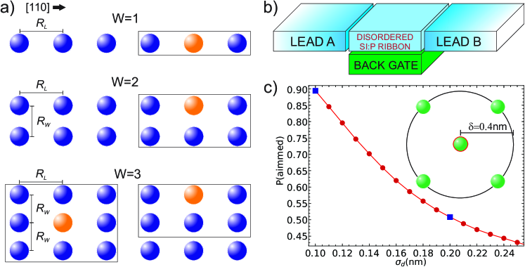
We characterize the nanostructures by four geometric parameters, namely, width (), length (), transversal donor distance () and longitudinal donor distance (), see Fig. 1(a). Considering the placement process to occur along the Si direction, the target P donors form a rectangular lattice with lattice parameters defined by and .
The model multi-orbital Hamiltonian written in the LCDO basis [8] reads
| (1) |
where () are creation (annihilation) operators of electrons at the orbital centered at the th site, is the corresponding number operator, is the onsite energy and the hopping term. In this equation comprises the sum over pairs of sites for which the hopping terms are not negligible: The summation is performed over sites inside rectangular regions like the ones in Fig. 1(a). For 1, 2 and 3 we take up to 2, 5 and 8 neighbors, respectively. The parameters were calculated within the LCDO scheme. In order to improve the reliability of the electronic calculations at smaler interdornor distances, we extend the treatment presented in Ref. [*[][fordetailsontheLCDOformalismseeSuppl.Mat.]Dusko2018] by including multi-orbitals and three-center corrections due to neighboring cores in the hopping energies. A detailed presentation is found in the Appendix. These developments allow us to accurately address the nanoribbon model ( sites) placement parameters ( and ) of the order of nm. We keep the isotropic approximation.
The model system we study consists of a central region, corresponding to the disordered Si:P nanostructure coupled to leads in thermal and chemical equilibrium with electronic reservoirs, see Fig. 1(b). The leads are semi-infinite, translational invariant and define the electronic bands density of states coupled to the system of interest [11]. In addition, we investigate the effect of a uniform back gate potential, and study its applicability to control the nanostructure transport properties. The gate potential is included in the model as a correction to the onsite energy, namely, . Here is the shift in the electronic states energy and is the unbiased onsite energy calculated within the LCDO scheme. The energy gained by the electron is , where is the gate potential, is the electron charge, and is a sample-dependent constant incorporating the Si dielectric screening, geometry and the capacitive coupling of the donor electron with other leads in the system. We expect that some trends for a lateral gate potential as the one present in Ref. [2, 3] can be inferred by comparing different nanoribbon widths, as a confining lateral potential decreases the effective .
We study the impact of positional disorder in such systems using a Gaussian disorder model. The disorder is quantified by two parameters, namely, a cutoff radius around a target substitutional site and the position standard deviation . For simplicity, we choose nm, in which case each donor can be placed at 5 different Si sites. The degree of disorder is controlled by . Figure 1(c) gives the dependence of the distribution of the implanted ion positions on . The main panel shows the probability distribution of an implanted donor to occupy the aimed position as a function of and the inset gives a graphical representation of the disorder cutoff radius . The values considered in this work, namely, nm and nm are indicated by the blue squares. These values are within state-of-the-art precision of STM atomic placement techniques [1, 6, 7].
We calculate the nanostructure linear conductance using the Landauer-Büttiker formula[12],
| (2) |
given in terms of the Fermi-Dirac distribution function and the electronic transmission [13]. In Eq. (2), is the retarded (advanced) Green’s function of the complete system (nanoribbon and leads), which we compute using the recursive Green’s function approach, implemented as in Refs. [11, 14, 15]. The th line or decay width, matrix elements are obtained from the embedding self-energy , where contains the coupling matrix elements of the sample with the th lead, while is the contact Green’s function. There are several ways to calculate the latter [16, 17, 18, 19], we compute by a standard decimation procedure based on renormalization-group ideas [20, 21].
We cast the nanostructures transport properties in terms of the localization length , formally defined by the wave function asymptotic behavior, . In this work, we infer the localization length by the analysis of the conductance at zero temperature.
III Transport and Placement
Si:P nanostructures are multi-path systems due to their multi-orbital nature. The hopping term in this multi-orbital framework plays an extremely non-trivial role, opening and closing channels depending on the system parameters. To improve the understanding of such system towards applications in nanodevices control, we investigate how the disorder and placement parameters affect conductance and localization.
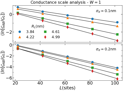
According to the localization theory in disordered systems [22], the conductance is expected to decrease exponentially with the ratio between the sample length and the localization length . Hence, we extract from the relation , where is an ensemble average (here typically over realizations). Figure 2 shows few representative examples of versus and the corresponding linear fit that gives .
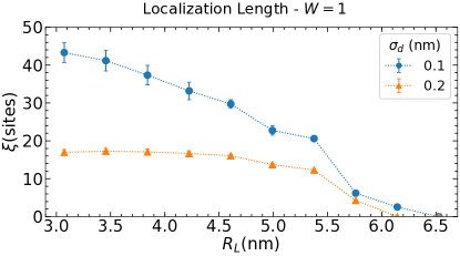
In Fig. 3 we present the localization length for (nanochains) behavior with for two levels of disorder. As expected, increasing or the disorder level lowers . Note that for small we observe an enhanced sensitivity of with . For these two disorder levels, shows an abrupt fall around nm.
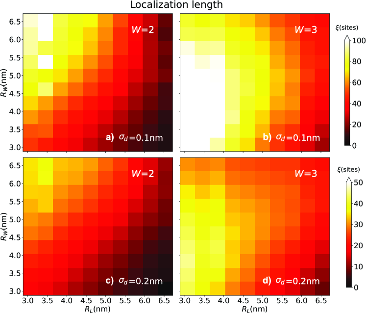
In order to represent the combined effect of the geometric parameters and in the transport trends of our system, we calculate the localization length for nm nm and, for each pair of parameters, is represented by the given color code. In Fig. 4(a) and (b) we present plots for disorder nm and in Fig. 4(c) and (d) nm. The frames on the left refer to and on the right to . The results suggest a metal-insulator phase diagram with a very similar overall behavior for both disorder intensities presented. In Fig. 4 (a) and (c) our simulations reveal a relatively small region in the investigated parameter space with non-monotonic behavior, roughly nm and nm. In particular, is peaked at nm and , and nm. Outside this non-trivial region, by increasing or decreasing the electronic states tend to become more localized. In Fig. 4 (b) and (d) we find an overall increase of and a wider region with non-trivial extended states, corresponding to the parameter range defined by nm and nm. In particular, shows peaks for nm and , and nm. Out of this non-trivial region, increasing or decreasing favors localization.
Comparing , and we observe an overall increasing in localization length with the system width, consistent with the increasing in the maximum number of transport channels, respectively , and . The sensitivity of on the disorder intensity seems to become stronger for larger values of .
IV Tuning Localization Length
The non-monotonic behavior of the localization length with the lattice geometry, namely and , suggests that one can tune it, and hence control the system’s conductance by a suitable external handle. In what follows we show that a back gate potential, as described in Sec. II, is capable to dramatically modify the transport properties of disordered Si:P nanowires. We recall that for electrons, .
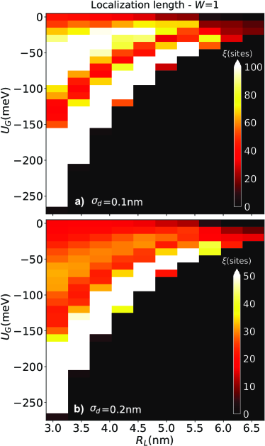
In order to get some insight on the gate control over localization lengths in nanoribbons, we start with the nanowire case, . Results for under a gate bias from 0 down to meV are presented in Fig. 5 for two degrees of disorder. For a fixed interdonor distance, according with the smaller(larger) degree of disorder oscillates in a larger(smaller) range in the graph truncated to () nm. Given that the P donor in Si lower energy levels are meV below the bottom of the Si conduction band edges, applying a bias of meV would ionize the donors completely inside the active (sample) region. A wider range of control is provided for negative values of which increases separation of the P electrons levels to the Si conduction band edge, thus remaining operational for the wide range shown in the figures. Therefore we restrict our results to . This effect can be explained as follows: rigidly shifts the nanowire energy spectrum. Hence, drives localized and extended states, as well as small and large density of states of the disordered system across the Fermi energy fixed by the contacts. The parameter range for a conducting behavior () shrinks for increasing values of , consistent with the drop in the mean value of the hopping matrix elements. An extensive analysis (not shown here) suggests a similar behavior with for different disorder intensities.
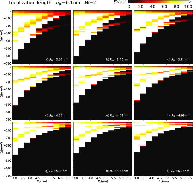
The case and nm is illustrated in Fig 6. The simulations indicate an overall increase of as a function of followed by an oscillatory pattern. As in the case we observe that the range corresponding to conducting behavior shrinks with . In addition, a similar feature can be observed for increasing values of . By varying for different values, we find the formation of a gap – a region of negligible values of – followed by a “reactivation” in the localization phase diagram for larger values of . This gap is highlighted in Fig. 6(a)-(c) where the threshold values are nm, nm and nm, respectively. The gap threshold value continues to increase monotonically along Fig. 6(d)-(f). In the last 3 panels [Fig. 6(g)-(i)], the gap closes resembling the signature of the case. Although it is reasonable to recover a phase diagram similar to case while increasing , we observe an enhancement in the overall localization length values and range leading to conducting behavior.
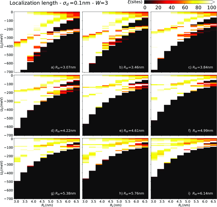
The wider ribbon case, , is given in fig. 7. As in and cases, one observes an increase in with followed by an oscillatory pattern and that the range leading to conducting behavior shrinks with and interdonor distances. For smaller values, Fig. 7(a)-(c) shows a larger gap than in the case and the opening of a second gap. Throughout Fig. 7(d)-(f) we observe that this second gap is short-lived comparing the first one. In summary, we find that both and range leading to conducting behavior are overall larger than in the and cases.
We have also performed calculations for nm, for both and , not shown since all properties follow the trends identified in the previous cases.
V Conductance control
In this section, we investigate the use of a gate potential as an external control of conductance for Si:P nanostructures. We set sites for the purpose of investigating a nanoswitch implementation in a length comparable to some experimental realizations[1, 2, 3] of higher P density.
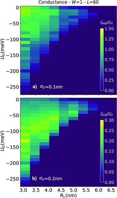
Figure 8 shows the average conductance as a function of and for nanochains (), The results show oscillations in as a function of both and . A minimum in occurs around nm, which should be avoided in practical implementations of the system as a nanoswitch. Oscillations due to stand out for smaller values. In line with the localization length analysis, an increase of causes the range of values corresponding to a conducting behavior to shrink. For nm, introducing a gate potential, we observe an increase in of approximately and for nm and nm, respectively.
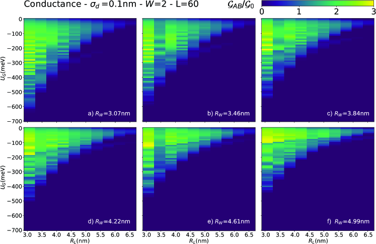
The conductance for sites nanoribbons and nm results, presented in Fig. 9, show a rapidly oscillatory behavior as a function of for small values, see Fig. 9(a)-(b). For larger values however [see Fig. 9(e)-(f)] the oscillations are strongly damped for small . In all cases, it is possible to observe a transition edge between larger and smaller values regimes. There is also a minimum in around nm, the feature is more pronounced in the cases shown in Fig. 9(b)-(e). We observe a very subtle gap opening in while increasing . The value corresponding to this opening increases with . In Fig. 9(a), (c) and (e) the corresponding gapping opening value is , and nm, respectively. As in the case, introducing a gate potential induces an increase of approximately 50% in .
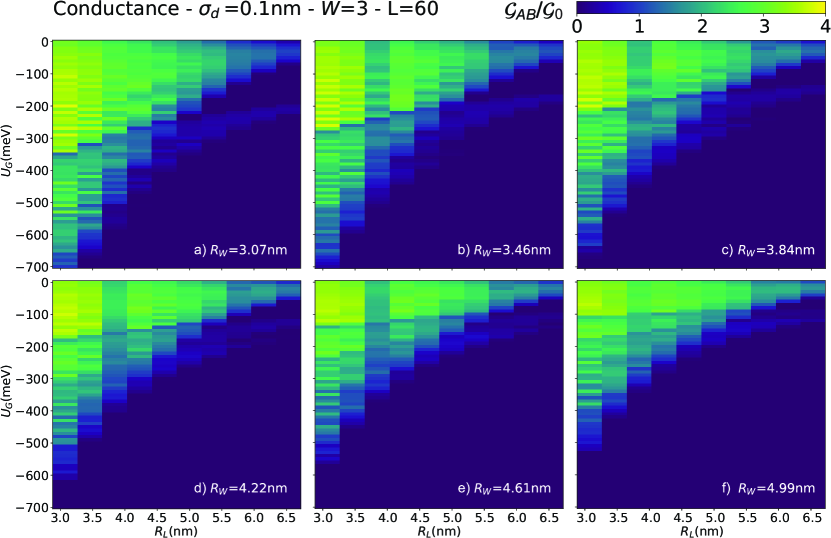
The results for nanoribbons of sites are presented in Fig. 10. Some similarities with case can be observed: Rapidly oscillating spectrum with a clear change in overall behavior in a given transition edge, for an example see Fig. 10(a) at nm and meV. In contrast with the case we observe two gap openings and an overall minimum in values around nm. The first gap can be observed in Fig. 10(a), (c) and (e) for , and nm, respectively. The second gap is more subtle but can be observed in Fig. 10(d) for nm, for example.
In summary, by considering nanostructures with increasing width, , and , we observe a corresponding increase in: (i) the overall values; (ii) the window of values leading to a conducting behavior; and (iii) in the number of gap openings. We also observe a change in the value corresponding to an overall minimum in . We also find that the overall behavior of the localization length on the lattice parameters does not depend on the disorder strength. This can be explicitly seen for the case by comparing the simulations for nm and nm.
Finally, let us stress the sharp driven metal-insulator transition appearing for any given choice of in all cases we analyze in this work. This remarkable feature strongly suggest that Si:P nanostructures can act as switches by properly tuning the gate potential.
VI Discussions and Conclusions
In this work we extended the LCDO formalism [8, 10] to include Gaussian disorder, a multi-orbital description and technical improvements, specified in the Appendix, which results in a more realistic description of P nanochains and to access nanoribbons of arbitrary widths. Our simulations treat the problem considering realistic system sizes and disorder. We also have put forward a proposal for an external control of transport properties such as localization length and conductance suggesting a new path of investigations for future experimental implementations.
We have found nontrivial features of the electronic transport properties due to system fabrication specifications still remaining robust against disorder. Specific values of placement parameters and nanostructure width provide optimized localization length, favoring high conductance. Our calculations indicate that a similar behavior is expected for different disorder levels.
We further analyze the effects of an external back gate potential to localization length and conductance. Properly tuning one can control localization lengths, allowing donor nanowires to keep current-carrying wave functions even for relatively long samples, serving as efficient connectors among nanodevices parts. In addition, it is possible to increase the nanostructure conductance, or decrease it by using this external potential, which suggests the use of such structures as nanoswitches. Both connectors and switches provide state-of-the-art resources contributing to nanodevices technology development.
Acknowledgements.
The authors acknowledge the financial support of the Brazilian funding agencies CL CNPq (grant 308801/2015-6); BK CNPq (grant 304869/2014-7) and FAPERJ (grant E-26/202.767/2018). This study was also financed in part by the Coordenação de Aperfeiçoamento de Pessoal de Nível Superior - Brazil (CAPES) - Finance Code 001. *Appendix A Microscopic model - Technical details
A.1 Linear Combination of Dopant Orbitals (LCDO)
Following the well established Kohn and Luttinger prescription [23, 24, 9] for shallow donors in Si, we consider a basis of six donor orbitals per site, corresponding to the six minima in Si conduction band. Valley orbit coupling, included by first order perturbation theory for degenerate states [25, 26], renders donor orbitals as superpositions of pure valley states obtained by the effective mass approach:
| (3) |
where refer to the donor orbitals pinned to the donor coordinates . The constants and stand for the normalization and valley population (presented in Table 1), is for simplicity approximated as an isotropic hydrogen-like envelope function, with a species dependent effective Bohr radius ( nm for Si:P) and are the Bloch functions of the 6 Si conduction band degenerate minima (). The latter are located along the equivalent directions , , at , where is the conventionally called Si lattice parameter [27]. The effective Bohr radius is obtained by incorporating screening effects due to the Si host charge carriers in the donor singular potential.
| (meV) | ||||||||
| A1 | 1 | 1 | 1 | 1 | 1 | 1 | -45.58 | |
| T | 0 | 0 | 0 | 0 | 1 | -1 | ||
| T | 0 | 0 | 1 | -1 | 0 | 0 | -33.90 | |
| T | 1 | -1 | 0 | 0 | 0 | 0 | ||
| Exy | 1 | 1 | -1 | -1 | 0 | 0 | -32.60 | |
| Ez | 1 | 1 | 1 | 1 | -2 | -2 |
Screening effects are included through a potential that interpolates the expected behavior for large and small values of , namely,
| (4) |
the screening length defines the transition between a bare and a screened potential. Here and are respectively the free space and the static relative permittivities.
As in previous works [8, 10] the Hamiltonian terms are calculated by the atomistic Hamiltonian , where is the single donor Hamiltonian and is the perturbation due to neighboring donor cores. We project the donor orbital to this atomistic Hamiltonian to extract the onsite and hopping terms. For the onsite term we obtain,
| (5) |
where is the single donor level energy given in Table 1, which contains valley-orbit corrections.
Similarly the hopping reads,
| (6b) | |||||
| (6c) | |||||
| (6d) | |||||
| (6e) | |||||
where is the interdonor distance, is the donor ground state energy, comes from the valley interference, and depends on the envelope overlap function and on two-centers () and three-centers () envelope function integrals. The integrals have a closed analytical solution [10], while the are calculated numerically. The labels all cores in the neighborhood of the and donors, see Fig. 1a.
Comparisons with experiments show that this multivalley central cell corrected dopant approximation gives an accurate description of the single impurity spectrum[26] and the corresponding wave functions[28], as well as the two impurities spectra in ionized[29] and neutral excited states[30]. The computationally advantage is clear: By incorporating the Si matrix explicitly in the orbitals, this approach allows the investigation of shallow donor systems of mesoscopic dimensions, a prohibitive task for a full atomistic approach.
A.2 Gaussian Expansion - Three-center Integrals
In this paper we consider hopping terms due to all neighboring cores. Since the straightforward calculation of these three-center integrals is computationally expensive, we write the envelope orbitals and the Coulomb potential, as a Gaussian expansion, namely
| (7) | |||||
| (8) |
where the coefficients , , , and are obtained by a standard least square fit and presented in Table 2. We find that by taking Gaussian terms, the expansions agree within accuracy for all values of where the target function satisfies .
A.3 Gaussian Coulomb Integrals - Product Rule
Let us now show the main derivation steps to obtain very simple expressions for the Gaussian integrals introduced above. The Gaussian expansion of the Coulomb three-center integral reads
where is the relative position to donor .
Let us now use the Gaussian product rule, i.e.,
| (10) |
where the constants and are the total and reduced exponents, while and are the relative and the Gaussian center of mass positions. Equation (10) expresses the product of two Gaussians in a new product where the first term is a constant and only the second term depends on . In other words, the problem is reduced to a two-center integral
| (11) |
When is a screened Coulomb potential, this two-centers integral can be decomposed in two terms, i.e. . The Gaussian expansion of the exponential term in the gives
The next step consists in writing as Gaussian integral, namely, . After rearranging the integrals and applying the product rule in the term, one obtains
where , , and where . Applying the product rule, as in Eq. (10), we find
where and
where and . As in Eq. (10), the spatial integrals depend only in the Gaussian center of mass and .
Finally, adjusting the integration limit in the remaining integrals, we obtain the simple expressions
By introducing the change of variables and the integrals are conveniently written as
where is called zero degree Boys function [31, 32]. To optimize computational resources we choose to solve the integral once, with high precision and in a range covering small and large values, and to adjust a curve that interpolates with rapidly decaying exponentials the expected behavior in all domain.
| (13) |
The coefficients of the fitted curve are presented in Table 3. For the domain we considered, , we find that , confirming the fitting quality.
| coefficient | fitted value |
|---|---|
References
- Weber et al. [2012] B. Weber, S. Mahapatra, H. Ryu, S. Lee, A. Fuhrer, T. C. G. Reusch, D. Thompson, W. C. T. Lee, G. Klimeck, L. C. L. Hollenberg, and M. Y. Simmons, Science 335, 64 (2012).
- Weber et al. [2014] B. Weber, H. Ryu, Y.-H. M. Tan, G. Klimeck, and M. Y. Simmons, Phys. Rev. Lett. 113, 246802 (2014).
- Shamim et al. [2016] S. Shamim, B. Weber, D. W. Thompson, M. Y. Simmons, and A. Ghosh, Nano Lett. 16, 5779 (2016).
- Schofield et al. [2003] S. R. Schofield, N. J. Curson, M. Y. Simmons, F. J. Rueß, T. Hallam, L. Oberbeck, and R. G. Clark, Phys. Rev. Lett. 91, 136104 (2003).
- Fuechsle et al. [2012] M. Fuechsle, J. A. Miwa, S. Mahapatra, H. Ryu, S. Lee, O. Warschkow, L. C. L. Hollenberg, G. Klimeck, and M. Y. Simmons, Nat. Nanotechnol. 7, 242 (2012).
- Zwanenburg et al. [2013] F. A. Zwanenburg, A. S. Dzurak, A. Morello, M. Y. Simmons, L. C. Hollenberg, G. Klimeck, S. Rogge, S. N. Coppersmith, and M. A. Eriksson, Rev. Mod. Phys. 85, 961 (2013).
- Salfi et al. [2016] J. Salfi, J. A. Mol, R. Rahman, G. Klimeck, M. Y. Simmons, L. C. L. Hollenberg, and S. Rogge, Nat. Commun. 7, 11342 (2016).
- Dusko et al. [2016] A. Dusko, A. L. Saraiva, and B. Koiller, Phys. Rev. B 94, 115425 (2016).
- Kohn [1957] W. Kohn, Shallow Impurity States in Silicon and Germanium, edited by F. SEITZ and D. TURNBULL, Solid State Physics, Vol. 5 (Academic Press, New York, 1957) pp. 257 – 320.
- Dusko et al. [2018] A. Dusko, A. Delgado, A. Saraiva, and B. Koiller, npj Quantum Inf. 4, 1 (2018).
- Lewenkopf and Mucciolo [2013] C. H. Lewenkopf and E. R. Mucciolo, J. Comput. Electron. 12, 203 (2013).
- Datta [1997] S. Datta, Electronic Transport in Mesoscopic Systems (Cambridge University Press, Cambridge, 1997).
- Meir and Wingreen [1992] Y. Meir and N. S. Wingreen, Phys. Rev. Lett. 68, 2512 (1992).
- Ridolfi et al. [2017] E. Ridolfi, L. R. F. Lima, E. R. Mucciolo, and C. H. Lewenkopf, Phys. Rev. B 95, 035430 (2017).
- Lima et al. [2018] L. Lima, A. Dusko, and C. Lewenkopf, Phys. Rev. B 97, 165405 (2018).
- Lopez Sancho et al. [1985] M. P. Lopez Sancho, J. M. Lopez Sancho, and J. Rubio, J. Phys. F: Met. Phys. 15, 851 (1985).
- A. MacKinnon [1985] A. MacKinnon, Z. Phys. B 59, 385 (1985).
- Rocha et al. [2006] A. R. Rocha, V. M. García-Suárez, S. Bailey, C. Lambert, J. Ferrer, and S. Sanvito, Phys. Rev. B 73, 085414 (2006).
- Wimmer [2009] M. Wimmer, Quantum transport in nanostructures: From computational concepts to spintronics in graphene and magnetic tunnel junctions, Ph.D. thesis, University Regensburg (2009).
- da Silva and Koiller [1981] C. E. T. G. da Silva and B. Koiller, Solid State Commun. 40, 215 (1981).
- Robbins and Koiller [1983] M. O. Robbins and B. Koiller, Phys. Rev. B 27, 7703 (1983).
- Sheng [2006] P. Sheng, Introduction to Wave Scattering, Localization and Mesoscopic Phenomena (Springer-Verlag Berlin Heidelberg, Heidelberg, 2006).
- Luttinger and Kohn [1955] J. M. Luttinger and W. Kohn, Phys. Rev. 97, 869 (1955).
- Kohn and Luttinger [1955] W. Kohn and J. M. Luttinger, Phys. Rev. 98, 915 (1955).
- Koiller et al. [2002] B. Koiller, X. Hu, and S. Das Sarma, Phys. Rev. B 66, 115201 (2002).
- Saraiva et al. [2015] A. L. Saraiva, A. Baena, M. J. Calderón, and B. Koiller, J. Phys.: Condens. Matter 27, 154208 (2015).
- Madelung [2012] O. Madelung, Semiconductors: data handbook (Springer Science & Business Media, 2012).
- Saraiva et al. [2016] A. Saraiva, J. Salfi, J. Bocquel, B. Voisin, S. Rogge, R. B. Capaz, M. Calderón, and B. Koiller, Phys. Rev. B 93, 045303 (2016).
- Gonzalez-Zalba et al. [2014] M. F. Gonzalez-Zalba, A. Saraiva, M. J. Calderón, D. Heiss, B. Koiller, and A. J. Ferguson, Nano Lett. 14, 5672 (2014).
- Dehollain et al. [2014] J. P. Dehollain, J. T. Muhonen, K. Y. Tan, A. Saraiva, D. N. Jamieson, A. S. Dzurak, and A. Morello, Phys. Rev. Lett. 112, 236801 (2014).
- Boys and Egerton [1950] S. Boys and A. Egerton, Proc. Roy. Soc. 200, 542 (1950).
- Gill [1994] P. M. Gill (Academic Press, 1994) pp. 141 – 205.