Single-photon light emitting diodes based on pre-selected quantum dots using a deterministic lithography technique
Abstract
In the present study, we developed a fabrication process of an electrically driven single-photon LED based on InP QDs emitting in the red spectral range, the wavelength of interest coinciding with the high efficiency window of \ceSi APDs. A deterministic lithography technique allowed for the pre-selection of a suitable QD, here exclusively operated under electrical carrier injection. The final device was characterized under micro-electroluminescence in direct current, as well as in pulsed excitation mode. In particular, under pulsed excitation of one device, single-photon emission of a spectral line, identified as an exciton, has been observed with , where the non-zero -value is mainly caused by background contribution in the spectrum and re-excitation processes due to the electrical pulse length. The obtained results constitute an important step forward in the fabrication of electrically driven single-photon sources, where deterministic lithography techniques can be used to sensibly improve the device performances. In principle, the developed process can be extended to any desired emitter wavelength above up to the telecom bands.
In the development of photonic-based quantum technology, several systems have been under discussion as sources of single and entangled photons. Among several possibilities, semiconductor quantum dots (QDs) showed the capability of generating very pure single and indistinguishable photonsDing et al. (2016); Somaschi et al. (2016) as well as highly entangled photon pairsHuber et al. (2018). Despite state-of-the-art performances have been reached under optical pumping, the possibility of implementing an efficient electrical pumping scheme will be of key importance for device scalability. An electrically-driven device would have an overall smaller footprint and its performances would not be affected by time dependent instabilities of the pumping conditions, as it may happen with a spatial or spectral drift of the excitation laser. Electrically driven single-photon devices have been experimentally demonstrated, covering the spectrum from the blue up to the telecom regimesYuan et al. (2002); Deshpande et al. (2013); Reischle et al. (2008); Kessler et al. (2012); Heindel et al. (2012); Ward et al. (2007); Müller et al. (2018). Additionally, pulse generators can be used for electrical carrier injection reaching on-demand operationReischle et al. (2010); Zhang et al. (2015); Heindel et al. (2012) with high excitation repetition rates up to Hargart et al. (2013). Thus, high flexibility in terms of pumping conditions can be achieved, tailoring the emission properties to match the application needs. This makes them a very versatile choice for complex experiments in the field of quantum information technology Knill et al. (2001); O’Brien et al. (2009); Waks et al. (2002) and metrology applications, which will largely benefit from a light source which provides a stable and reliable photon flux. Furthermore, since QDs are embedded in a semiconductor matrix, well established semiconductor processing techniques can be applied for their implementation into cavitiesUnsleber et al. (2016); Somaschi et al. (2016); Ates et al. (2012); Pelton et al. (2002); Gérard et al. (1998) and various photonic structuresReimer et al. (2012); Claudon et al. (2010); Munsch et al. (2013); Trojak et al. (2017); Gschrey et al. (2015); Sartison et al. (2017, 2018) to enhance their performances. For this purpose, deterministic fabrication techniques were developed largely improving the fabrication yield due to the capability to localize an emitter and tailor the lithographically defined mask according to its emission propertiesSartison et al. (2017, 2018); Somaschi et al. (2016); Ates et al. (2012); Trojak et al. (2017); Gschrey et al. (2015); Unsleber et al. (2016). In this work, we based our device fabrication on in-situ photolithography aligned on an electrically pre-selected emitter. The use of electrical pumping, rather than the commonly utilized optical excitation, ensures that the emitters will have the desired performances after the device processing. Additionally, since optical excitation is not required, only two channels (collection and lithography) are necessary, in contrast to usual approaches Sartison et al. (2017); Dousse et al. (2008).
Single-photon light-emitting diodes (SPLEDs) based on InP QDs emitting in the red
spectral rangeKessler et al. (2012); Reischle et al. (2010) have shown their potential in realizing QKD experimentsHeindel et al. (2012).
Despite that, former demonstrations were limited by the non-deterministic device fabrication which turned out in SPLEDs including several QDs.
Only lowering the applied voltage allowed for the observation of emission from a single dot which is randomly placed into the large SPLED aperture.
Our newly developed method, enables us now to integrate electrically pre-selected QDs into similar optical devices while having a precise knowledge of the positionSartison et al. (2017) and the emission properties prior to the fabrication process.
Furthermore, the device size could be reduced and a smaller aperture diameter resulted in a more concentrated current confinement which enables a more efficient pumping of the pre-selected QD.
As a proof of principle, we verified the non-classical emission properties of one pre-selected integrated QD under triggered electrical excitation.
The processed sample was grown via metal-organic vapor-phase epitaxy (MOVPE).
It consists of a bottom n-doped distributed Bragg reflector (DBR) with 45 mirror pairs followed by the InP QD layer.
A high Al-containing oxidation layer was deposited before the structure was completed with a p-doped DBR containing 6 mirror pairs.
The oxidation layer is used during the device fabrication to ensure current confinement and selective excitation of individual QDs.
A detailed report on the sample structure can be found in Schulz et. alSchulz et al. (2011).


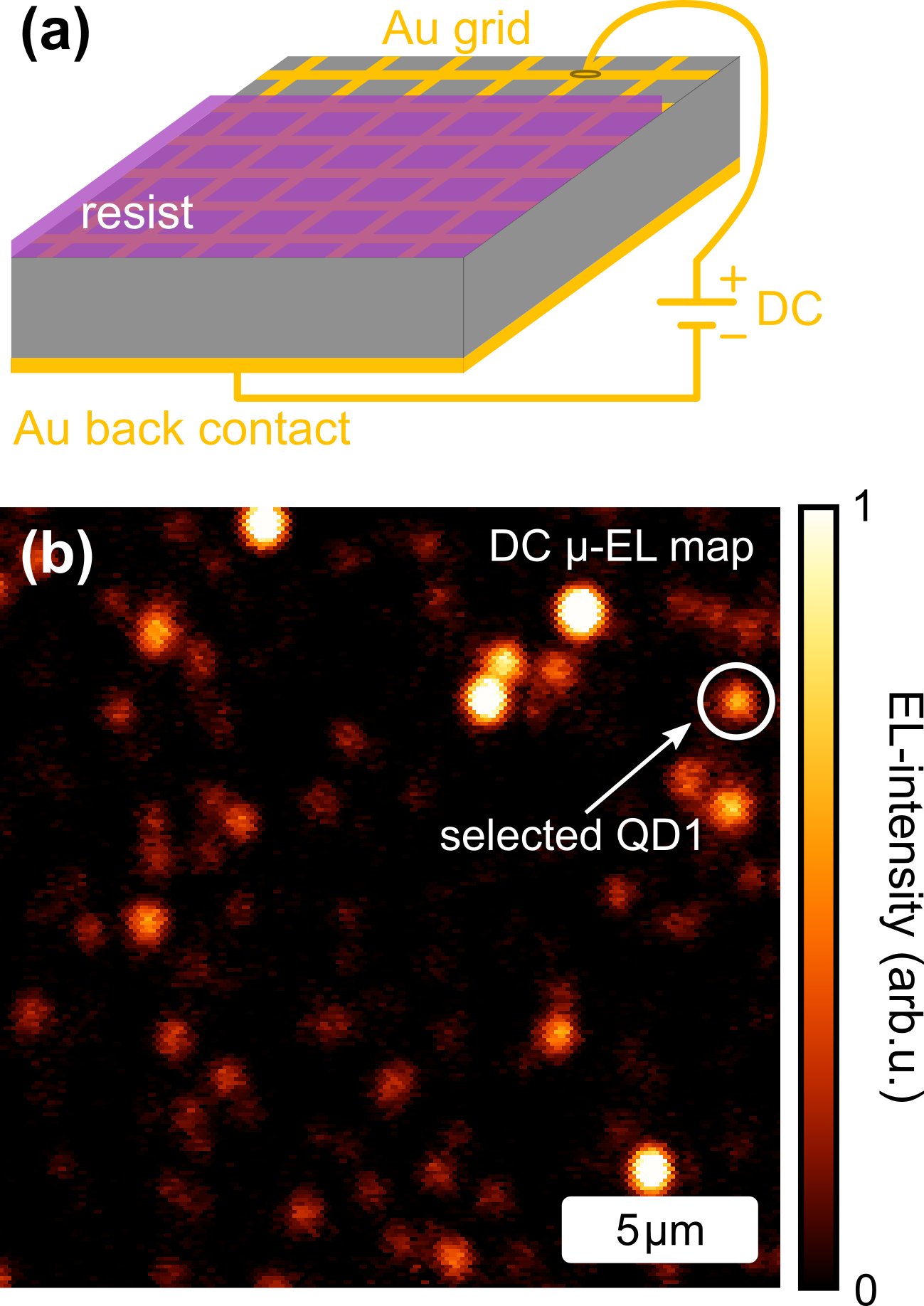
As a first process step, a grid was lithographically defined via standard UV photolithography, followed by electron-beam evaporation of a \ceCr and a \ceAu layer. The top of the sample then displays a grid similar to the one illustrated in Fig. 1(a), while the bottom is fully covered by these metallic layers to constitute the bottom contact. These contacts enable the observation of electroluminescence during the low-temperature deterministic lithography step. For this purpose, the sample was again spin-coated with a positive resist, partially exposed and developed to get access to the contact grid on top. After being mounted on an electrical sample holder, the partially exposed grid was contacted to the positive electrode via wire bonding (see sketched wire in Fig. 1(a)). For QD pre-selection, a commercially available low-temperature photolithography setup was used as already described in former worksDousse et al. (2008); Sartison et al. (2017, 2018). However, this time the QD excitation was provided by supplying a direct current (DC) source instead of optical excitation. This provides two advantages: on the one hand, it does not require the excitation laser to be carefully aligned with collection and lithography channels; on the other hand, it ensures that the pre-selected QD will also show emission in EL after the device processing. When cooled down to , -EL maps were acquired under DC excitation. Bright and isolated QD emission could be observed, despite a modest rise in sample temperature to (see Fig. 1(b)). This is due to the large current injection area but only has a modest effect on the dot emission propertiesReischle et al. (2008).
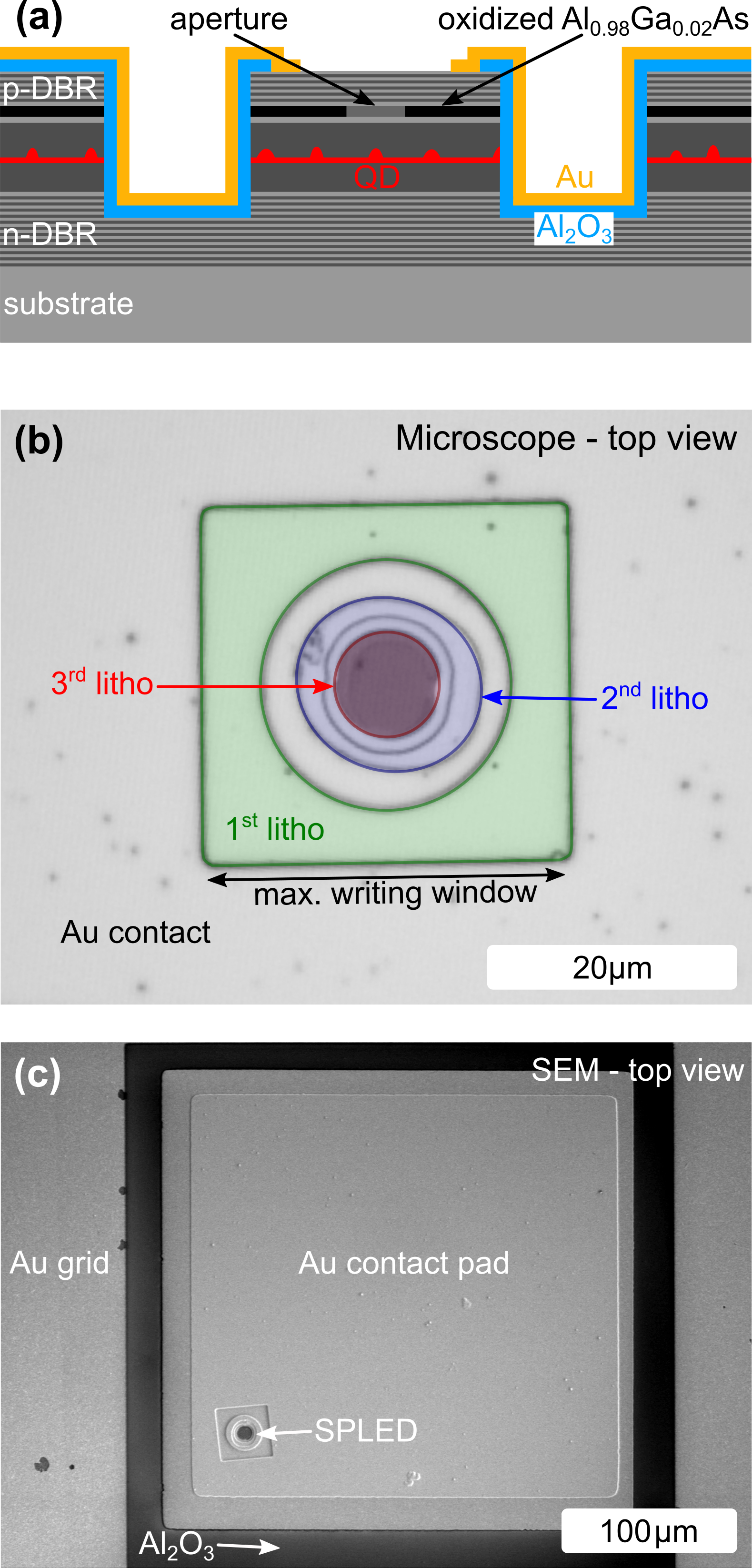
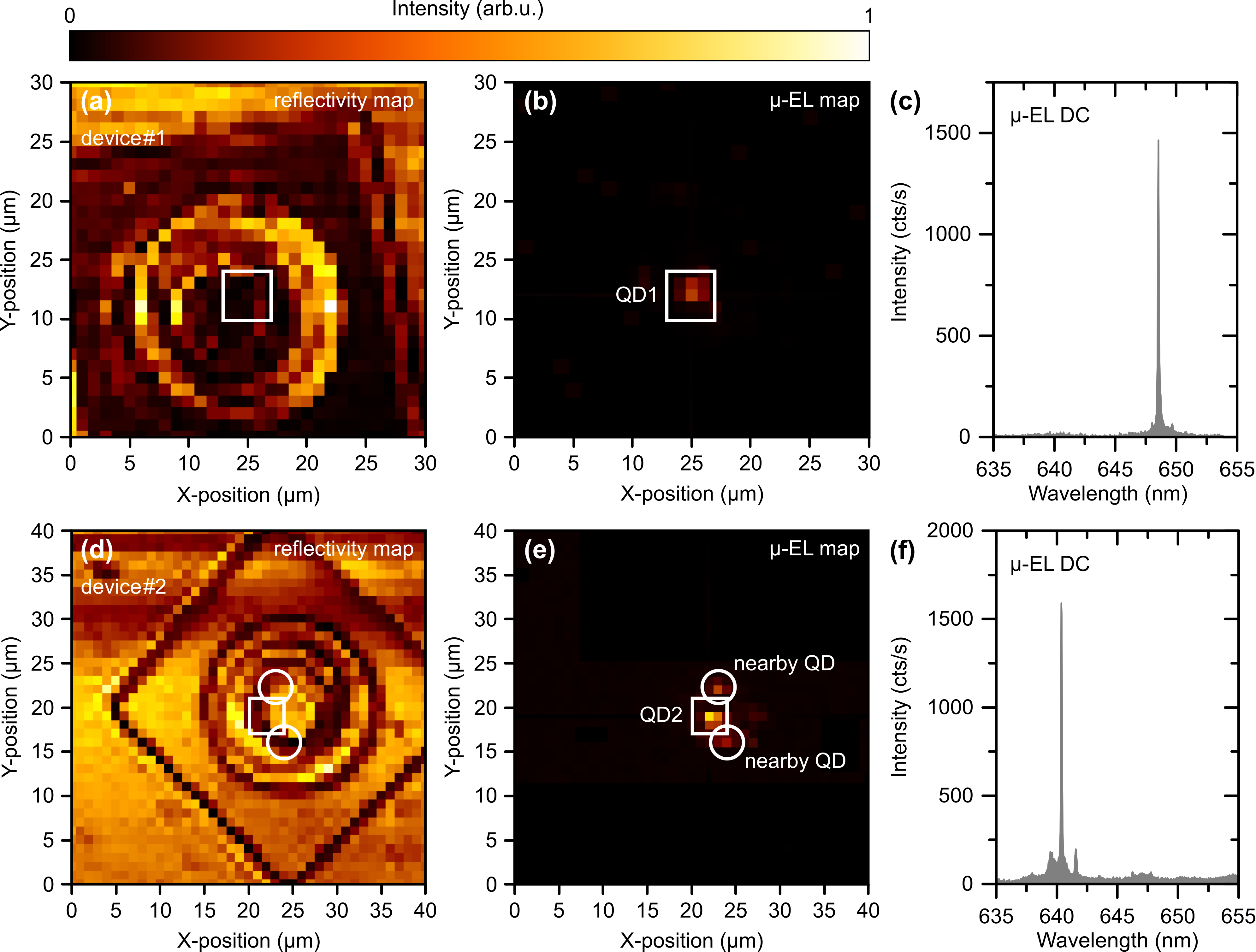
As soon as a spatially and spectrally isolated QD is identified, the device is processed, deterministically aligned on the spatial position of the QD, as described in the following (a detailed sketch of the fabrication steps can be found in Fig. S1 in the supplementary material). Fig. 2(a) illustrates the final device in cross section. In order to realize such a structure, a writing window of was exposed at low temperature around the QD except a circle with a diameter of approximately (marked as litho in Fig. 2(b)). The unexposed resist which remains after the development served as an etching mask which was transferred into the sample structure via inductively-coupled reactive-ion etching using \ceSiCl4:\ceAr. The etching should not be stopped before reaching the bottom DBR. This gives lateral access to the high aluminum containing layer, providing the possibility of later wet-chemical aperture oxidation. At this point, the sample was covered again with resist, this time with an image reversible one, and placed in the in-situ lithography setup. Since the position of the QD is already marked by the device itself, i.e. the emitter is located in the center of the etched structure, the second lithography could be carried out at room temperature. A red laser at , aligned to be collinear with the lithography channel, was scanned over the device and the reflectivity was mapped via a photodiode using the back reflected laser signal (see Fig. S2 in the supplementary material). Based on this map, the position and size of the circle to be exposed was determined. Here, the diameter of the second lithography (Fig. 2(b) litho) was set to approximately . This size has to be smaller than the circle of the first lithography to ensure electrical insulation provided by the subsequently deposited \ceAl2O3 layer anywhere except in the center of the device (see blue layer in Fig. 2(a)). After the image reversal bake, flood exposure and development of the resist, \ceAl2O3 was deposited and a lift-off step was performed. This allows for the realization of an insulating layer all over the sample, except in the device central area, where the QD is sitting. In the following step, wet-chemical oxidation defined an aperture in the high aluminum containing layer of approximately in order to further limit the area of current flow (see Fig. 2(a)). QDs outside this aperture are not reached by the injected carriers. Optimally, when the QD density is low enough, it is possible to obtain emission of only one QD when the device is operated. The previously described lithographic step was repeated, but this time the exposed circle ( litho Fig. 2(b)) had to be smaller than the opening in the \ceAl2O3 (exposure diameter chosen to be around ). A grid was also exposed in standard UV lithography around the structures which defines the contact area for addressing each device individually via wire bonding. It followed the resist development, the contact deposition using \ceCr and \ceAu layers and a lift-off step. Figure 2(c) shows the device including the large gold contact pad, which is needed for wire bonding. After device fabrication, the sample was placed on a custom sample holder, suitable for DC and high-frequency pulsed electrical operation, and contacted via wire bonding. Thereafter, it was cooled down to in a helium flow cryostat. The first characterization step was devoted to verifying the successful fabrication. For this scope, reflectivity and electroluminescence in DC were simultaneously recorded. A very weak laser signal from a He-Ne laser was added to the DC bias during the mapping, which does not modify the electrically-pumped QD emission. This enabled to gather information about device topography (in reflectivity) and electrical emission (-EL) at the same time. By applying a spectral filter in the evaluation of the spectra, either the topography (Fig. 3(a) and (d)) or the QD emission (Fig. 3(b) and (e)) could be extracted.

Pre-selected QDs are marked with a square which yield also the brightest emission intensity. QDs nearby are marked with a circle. A fiber in the detection path was used as a pinhole for enhanced spatial resolution.
Each visible pixel corresponds to a recorded spectrum, as exemplary shown in Fig. 3. The respective QD position, within the collection spot size of around is marked in all maps, reflectivity and -EL. Here, a fiber was used in the detection path serving as a pinhole for a higher spatial resolution. For device , only the pre-selected QD was emitting inside the aperture. The corresponding spectrum is shown in Fig. 3(c). Device showed emission of two additional QDs together with the pre-selected one. However, the selected QD was the most central one as expected. In Fig. 3(f), the spectrum of QD2, the pre-selected one, is shown. It is important to mention that the oxidation step induced a significant compressive strain on the QD centered underneath the oxide aperture which resulted in a blue-shift of and for devices and , respectively. Thanks to this aperture, which forces the current flow around the QD, no detectable change of the device temperature was observed, differently from the operation during the first low-temperature lithography step.
Pulsed electrical pumping of the device was accomplished by a pulse generator suitable for narrow excitation pulse widths (EPW) and high excitation repetition rates (ERR). Its output was coupled to an amplifier to increase the peak voltage () up to a maximum of 5 V. With the use of a bias tee, an additional constant DC bias voltage () could be applied which was set slightly below the excitation threshold.
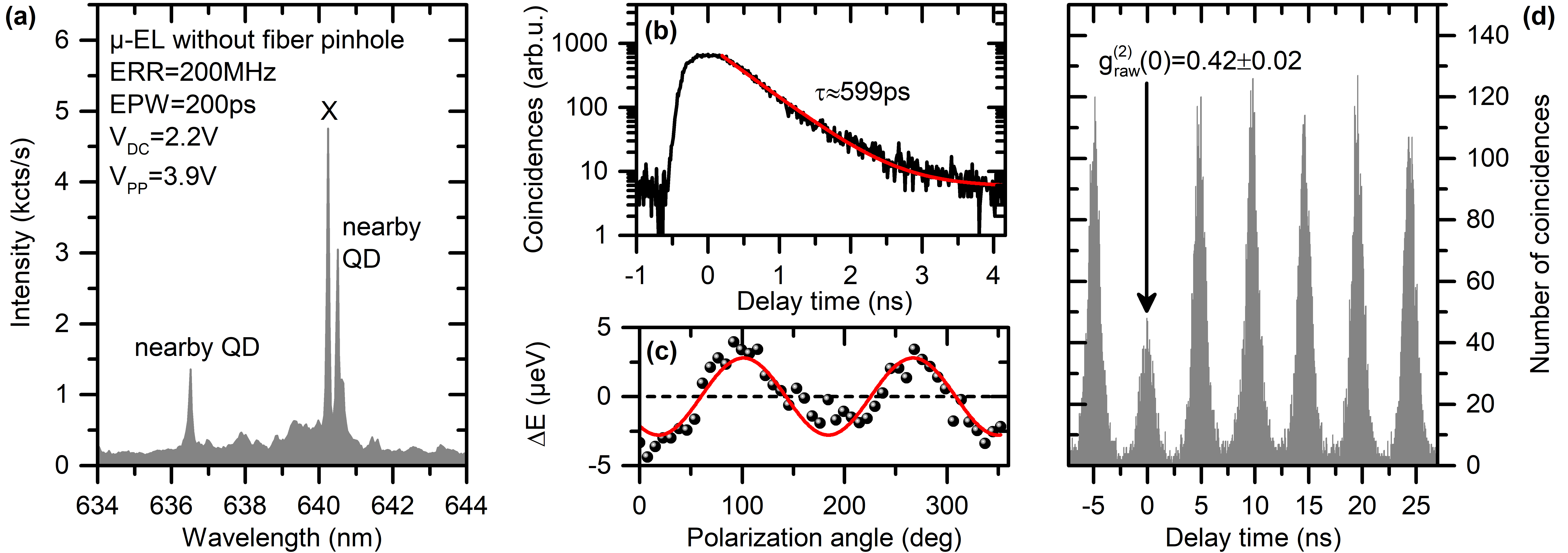
Pulsed excitation of device 2 with an ERR of and a pulse width of resulted in the spectrum displayed in Fig. 4(a).
In contrast to the map and spectrum in Fig. 3, no spatial filter was used here, i.e. light was sent in free space to the spectrometer to maximize the count rate on the APDs.
As a consequence, the EL intensity of the nearby QDs is slightly increased with respect to the intensity of the pre-selected QD (compare Fig. 3(f) and Fig. 4(a)).
The AC peak voltage was set to while the DC bias was kept at .

For the upcoming detailed measurements, the brightest emission line in Fig. 4 was chosen.
Time-correlated single-photon counting (TCSPC) revealed a decay time of (see Fig. 4(b)), a value typical for electrically driven InP QDsReischle et al. (2010). Polarization dependent measurements were performed on this line, which showed a spectral oscillation with an amplitude of around the central peak position marked as the dashed line in Fig. 4(c)).
This oscillation is an indication of a fine structure splitting of the line.
Considering the decay time of , the conclusion can be drawn that this line stems from an excitonic transition.
A second-order autocorrelation measurement on this emission line resulted in the histogram seen in Fig. 4(d). Integration of the coincidences within a temporal window of gave a raw value of
and a dark count corrected value of .
The non-perfect suppression of the zero-delay peak can be accounted to residual background emission as well as possible re-excitation during the same pulse.
A benchmark for the signal to background ratio could be obtained from fitting the spectrum to distinguish between the QD signal and the underlying background (see Kessler et al.Kessler et al. (2012)).
Thus, the could be background corrected via the formulaBrouri et al. (2000) ,
resulting in a value of
which compares with previously obtained resultsKessler et al. (2012) achieved with similar excitation pulse lengths.
Additionally, it has to be considered that the non-negligible tails in the Gaussian excitation pulse may induce re-excitation of the QD with consequent degradation of the .
Therefore, future measurements have to be performed using pulses with an EPW much shorter than in order to avoid re-excitation.
In conclusion, we realized a QD-based single-photon LED, operating at the absolute efficiency maximum of Si APDs, via an optimized deterministic fabrication technique. QDs were here pre-selected in -EL and the device was fabricated via state-of-the-art low temperature in-situ lithography and standard clean room fabrication techniques. The successful deterministic integration of QDs could be verified by the acquisition of -EL maps combined with reflectivity maps. Furthermore, the device performances were characterized under pulsed electrical excitation by means of EL polarization dependence, time-resolved EL decay time and photon-autocorrelation measurements. A decay time of under triggered electrical excitation compares well with already reported values for \ceInP QDs in literature. Additionally, a value of could be recorded, only corrected for the detector induced dark count contribution, thus indicating dominant single-photon emission. By accounting also for the spectral background contribution, a corrected value of could be estimated. The deterministic fabrication process of SPLEDs developed in this work can be applied to any electrically driven emitter from the red spectral range up to the telecom regimes. The proof of principle measurements presented here show the possibility of combining in-situ optical lithography with electrically driven non-classical light sources. It enables the route towards electrically driven cavity systems and high brightness devices. Improving the performances of single QD devices via deterministic lithography techniques will be of key importance in a range of quantum technology implementations, from quantum key distribution to quantum enhanced metrology.
The authors would like to thank the DFG for financial support via the project Mi500/27-1. S.K. and S.L.P. greatly acknowledge the Baden-Württemberg Stiftung “Post-Doc Elite Programm” via the project “Hybride Quantensysteme für Quantensensorik”. The research of the was financially supported by the Ministry of Science, Research and Arts Baden-Württemberg.
References
- Ding et al. (2016) X. Ding, Y. He, Z.-C. Duan, N. Gregersen, M.-C. Chen, S. Unsleber, S. Maier, C. Schneider, M. Kamp, S. Höfling, C.-Y. Lu, and J.-W. Pan, Physical Review Letters 116, 020401 (2016).
- Somaschi et al. (2016) N. Somaschi, V. Giesz, L. De Santis, J. C. Loredo, M. P. Almeida, G. Hornecker, S. L. Portalupi, T. Grange, C. Antón, J. Demory, C. Gómez, I. Sagnes, N. D. Lanzillotti-Kimura, A. Lemaítre, A. Auffeves, A. G. White, L. Lanco, and P. Senellart, Nature Photonics 10, 340 (2016).
- Huber et al. (2018) D. Huber, M. Reindl, S. F. Covre Da Silva, C. Schimpf, J. Martín-Sánchez, H. Huang, G. Piredda, J. Edlinger, A. Rastelli, and R. Trotta, Physical Review Letters 121, 33902 (2018).
- Yuan et al. (2002) Z. Yuan, B. E. Kardynal, R. M. Stevenson, A. J. Shields, C. J. Lobo, K. Cooper, N. S. Beattie, D. A. Ritchie, and M. Pepper, Science 295, 102 (2002).
- Deshpande et al. (2013) S. Deshpande, J. Heo, A. Das, and P. Bhattacharya, Nature Communications 4, 1675 (2013).
- Reischle et al. (2008) M. Reischle, G. J. Beirne, W.-M. Schulz, M. Eichfelder, R. Roßbach, M. Jetter, and P. Michler, Optics Express 16, 12771 (2008).
- Kessler et al. (2012) C. A. Kessler, M. Reischle, F. Hargart, W. M. Schulz, M. Eichfelder, R. Roßbach, M. Jetter, P. Michler, P. Gartner, M. Florian, C. Gies, and F. Jahnke, Physical Review B 86, 115326 (2012).
- Heindel et al. (2012) T. Heindel, C. A. Kessler, M. Rau, C. Schneider, M. Fürst, F. Hargart, W. M. Schulz, M. Eichfelder, R. Roßbach, S. Nauerth, M. Lermer, H. Weier, M. Jetter, M. Kamp, S. Reitzenstein, S. Höfling, P. Michler, H. Weinfurter, and A. Forchel, New Journal of Physics 14, 083001 (2012).
- Ward et al. (2007) M. B. Ward, T. Farrow, P. See, Z. L. Yuan, O. Z. Karimov, A. J. Bennett, A. J. Shields, P. Atkinson, K. Cooper, and D. A. Ritchie, Applied Physics Letters 90, 063512 (2007).
- Müller et al. (2018) T. Müller, J. Skiba-Szymanska, A. B. Krysa, J. Huwer, M. Felle, M. Anderson, R. M. Stevenson, J. Heffernan, D. A. Ritchie, and A. J. Shields, Nature Communications 9, 862 (2018).
- Reischle et al. (2010) M. Reischle, C. Kessler, W. M. Schulz, M. Eichfelder, R. Roßbach, M. Jetter, and P. Michler, Applied Physics Letters 97, 143513 (2010).
- Zhang et al. (2015) J. Zhang, J. S. Wildmann, F. Ding, R. Trotta, Y. Huo, E. Zallo, D. Huber, A. Rastelli, and O. G. Schmidt, Nature Communications 6, 10067 (2015).
- Hargart et al. (2013) F. Hargart, C. A. Kessler, T. Schwarzbäck, E. Koroknay, S. Weidenfeld, M. Jetter, and P. Michler, Applied Physics Letters 102, 011126 (2013).
- Knill et al. (2001) E. Knill, R. Laflamme, and G. J. Milburn, Nature 409, 46 (2001).
- O’Brien et al. (2009) J. L. O’Brien, A. Furusawa, and J. Vučković, Nature Photonics 3, 687 (2009).
- Waks et al. (2002) E. Waks, K. Inoue, C. Santori, D. Fattal, J. Vuckovic, G. S. Solomon, and Y. Yamamoto, Nature 420, 762 (2002).
- Unsleber et al. (2016) S. Unsleber, Y.-M. He, S. Gerhardt, S. Maier, C.-Y. Lu, J.-W. Pan, N. Gregersen, M. Kamp, C. Schneider, and S. Höfling, Optics Express 24, 8539 (2016), 1512.07453 .
- Ates et al. (2012) S. Ates, L. Sapienza, M. Davanco, A. Badolato, and K. Srinivasan, IEEE Journal of Selected Topics in Quantum Electronics 18, 1711 (2012).
- Pelton et al. (2002) M. Pelton, C. Santori, J. Vučković, B. Zhang, G. S. Solomon, J. Plant, and Y. Yamamoto, Physical Review Letters 89, 233602 (2002).
- Gérard et al. (1998) J. M. Gérard, B. Sermage, B. Gayral, B. Legrand, E. Costard, and V. Thierry-Mieg, Physical Review Letters 81, 1110 (1998).
- Reimer et al. (2012) M. E. Reimer, G. Bulgarini, N. Akopian, M. Hocevar, M. B. Bavinck, M. A. Verheijen, E. P. A. M. Bakkers, L. P. Kouwenhoven, and V. Zwiller, Nature Communications 3, 737 (2012).
- Claudon et al. (2010) J. Claudon, J. Bleuse, N. S. Malik, M. Bazin, P. Jaffrennou, N. Gregersen, C. Sauvan, P. Lalanne, and J.-M. Gérard, Nature Photonics 4, 174 (2010).
- Munsch et al. (2013) M. Munsch, N. S. Malik, E. Dupuy, A. Delga, J. Bleuse, J.-M. Gérard, J. Claudon, N. Gregersen, and J. Mørk, Physical Review Letters 110, 177402 (2013).
- Trojak et al. (2017) O. J. Trojak, S. I. Park, J. D. Song, and L. Sapienza, Applied Physics Letters 111, 021109 (2017).
- Gschrey et al. (2015) M. Gschrey, A. Thoma, P. Schnauber, M. Seifried, R. Schmidt, B. Wohlfeil, L. Krüger, J. H. Schulze, T. Heindel, S. Burger, F. Schmidt, A. Strittmatter, S. Rodt, and S. Reitzenstein, Nature Communications 6, 7662 (2015).
- Sartison et al. (2017) M. Sartison, S. L. Portalupi, T. Gissibl, M. Jetter, H. Giessen, and P. Michler, Scientific Reports 7, 39916 (2017).
- Sartison et al. (2018) M. Sartison, L. Engel, S. Kolatschek, F. Olbrich, C. Nawrath, S. Hepp, M. Jetter, P. Michler, and S. L. Portalupi, Applied Physics Letters 113, 032103 (2018).
- Dousse et al. (2008) A. Dousse, L. Lanco, J. Suffczyński, E. Semenova, A. Miard, A. Lemaître, I. Sagnes, C. Roblin, J. Bloch, and P. Senellart, Physical Review Letters 101, 267404 (2008).
- Schulz et al. (2011) W. M. Schulz, M. Eichfelder, M. Reischle, C. Kessler, R. Roßbach, M. Jetter, and P. Michler, Journal of Crystal Growth 315, 127 (2011).
- Brouri et al. (2000) R. Brouri, A. Beveratos, J.-P. Poizat, and P. Grangier, Optics Letters 25, 1294 (2000).