Magnetic Properties of Epitaxially-grown SrRuO3 Nanodots
Abstract
We present the fabrication and exploration of arrays of nanodots of SrRuO3 with dot sizes between 500 nm and 15 nm. Down to the smallest dot size explored, the samples were found to be magnetic with a maximum of the Curie temperature TC achieved by dots of 30 nm diameter. This peak in TC is associated with a dot-size-induced relief of the epitaxial strain, as evidenced by scanning transmission electron microscopy.
I Introduction
Nanostructures of complex functional materials provide an experimental platform to investigate novel physical phenomena if the characteristic device size reaches intrinsic length scales, such as the inelastic scattering length or the Fermi wavelength. For mean-field systems, especially semiconductors, confinement effects have been studied for decades and have already been implemented in widespread technological applications Ashoori (1996); Kastner (1993). Recently, a significant number of investigations have shown that such confinement of correlated systems in 2D Bibes, Villegas, and Barthelemy (2011), e.g., at interfaces Mannhart and Schlom (2010); Hwang et al. (2012); Baiutti et al. (2015), in thin films Yoshimatsu et al. (2011) or superlattices Bern et al. (2013), promises a variety of interesting advantages over their mean-field counterparts. Although novel electronic properties are expected Mannhart et al. (2016) if correlated systems are confined in fewer dimensions, i.e., to 1D and 0D, such systems have been explored only marginally.
This work focuses on the limiting case of spatial confinement into 0D objects, i.e., into quantum dots or artificial atoms. In Refs. 10 and 11 it was shown that such dots can be fabricated at the LaAlO3/SrTiO3 interface using surface-modification with an atomic force microscope (AFM) tip. Ion-beam based fabrication of magnetic SrRuO3 nanodots with diameters of about 80 nm has been reported in Ref. 12. In Ref. 13 the magnetization reversal in similar nanostructures of various sizes was studied by magnetic force microscopy. We here use the top-down approach based on epitaxial growth and electron-beam lithography that allows such objects to be fabricated with high precision and reproducibility. At the same time, the form and mutual arrangement of these objects may be chosen and varied as desired. The main challenge for fabricating such devices is to synthesize a highly pure material with low defect density that along with small sizes allows the formation of a coherent many-body electron wave function. However, it is well known that the patterning process causes local material damage and dead layers, which can significantly reduce the mean free path of the electrons Katine et al. (2003).
In order to study the material behavior upon confinement in nanodots, we chose SrRuO3 Koster et al. (2012) as a model system. SrRuO3 is a correlated conducting perovskite oxide with strong itinerant ferromagnetism (bulk Curie temperature TC K) and an intensively studied perovskite material. It exhibits orthorhombic symmetry at room temperature. The ferromagnetic properties of SrRuO3 depend highly on the material quality as well as on the film thickness Ishigami et al. (2015); Chang et al. (2009). Even slight variations of the stoichiometry or lattice parameters may lead to a significant change of magnetic properties Siemons et al. (2007); Lu et al. (2015); Thomas et al. (2017). Hence, SrRuO3 is a model system to study the relevance of dead-layer creation and how materials behave upon confinement within low-dimensional objects. We therefore prepared epitaxial SrRuO3 nanodots with various diameters and explored how the magnetic properties of the material depend on the size of the structures.
II Experimental Techniques
For the sample preparation, special care was taken to deposit SrRuO3 films of high purity and with the desired stoichiometry. Prior to SrRuO3 deposition, SrTiO3 substrates were terminated in situ in the growth chamber by thermal annealing at 1300 °C for 200 s at a molecular oxygen pressure of 0.08 mbar Jäger et al. (2018). Immediately after that, and in the same UHV chamber, SrRuO3 thin films were grown by pulsed laser deposition with a target-substrate distance of 56 mm. The substrate temperature during growth was 680 °C, and the molecular oxygen pressure in the chamber was kept at 0.08 mbar. The SrRuO3 target was ablated using a KrF excimer laser with a wavelength of 248 nm and an energy density on the target of 2.5 J/cm2. The nanodots were patterned using a commercial 100 keV electron beam lithography system (JEOL JBX6300) and CSAR (Allresist, AR-P 6200) as resist material. After resist development, a 20-nm layer of amorphous Al2O3 was deposited, which was then used as a hard mask for dry etching with Ar ions at an energy of 600 eV and a pressure of mbar. For a pattern design, we used rectangular arrays of dots, where the dot periodicity equalled two dot diameters. Arrays covered the entire substrate area, excluding edge regions. For 20-nm dots, dots were fabricated on each substrate.
Scanning transmission electron microscopy (STEM) specimens in cross-sectional orientation were prepared by focused ion beam (Zeiss CrossBeam XB 1540) cutting, then nanomilled at liquid nitrogen temperature (Fischione NanoMill Model 1040). STEM investigations were carried out using a spherical aberration-corrected microscope (JEOL JEM-ARM 200F) with a DCOR probe corrector (CEOS GmbH) at 200 kV.
III Results
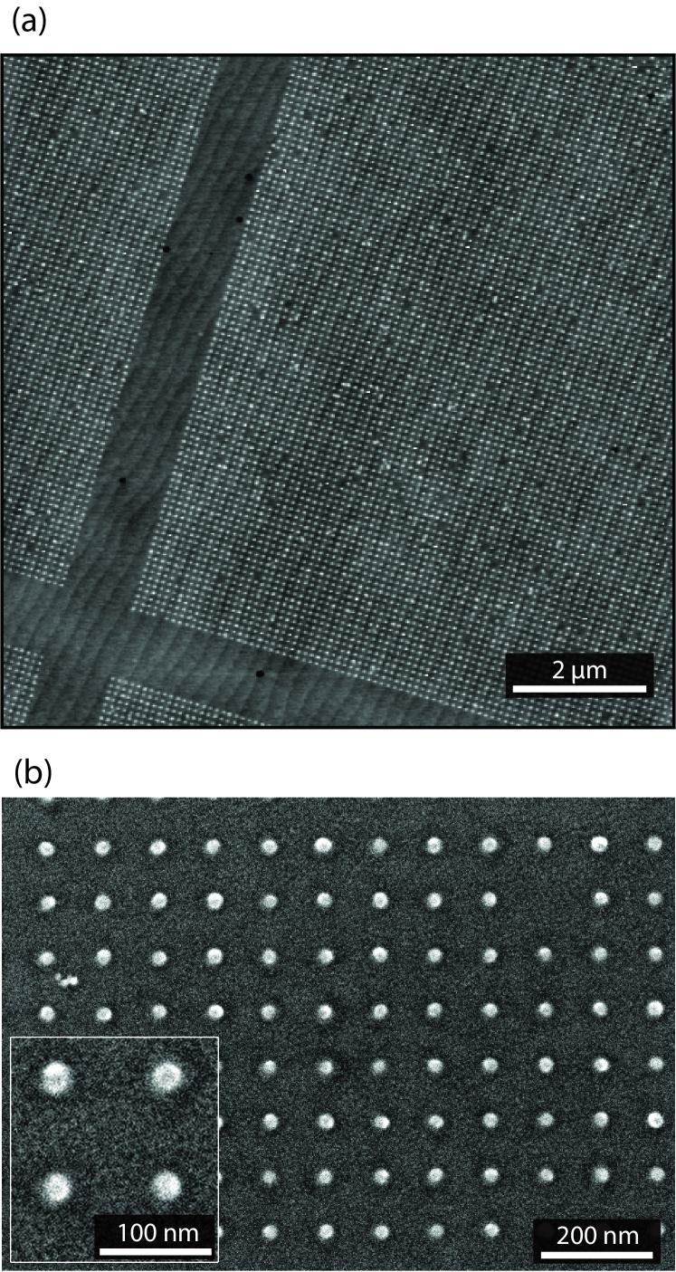
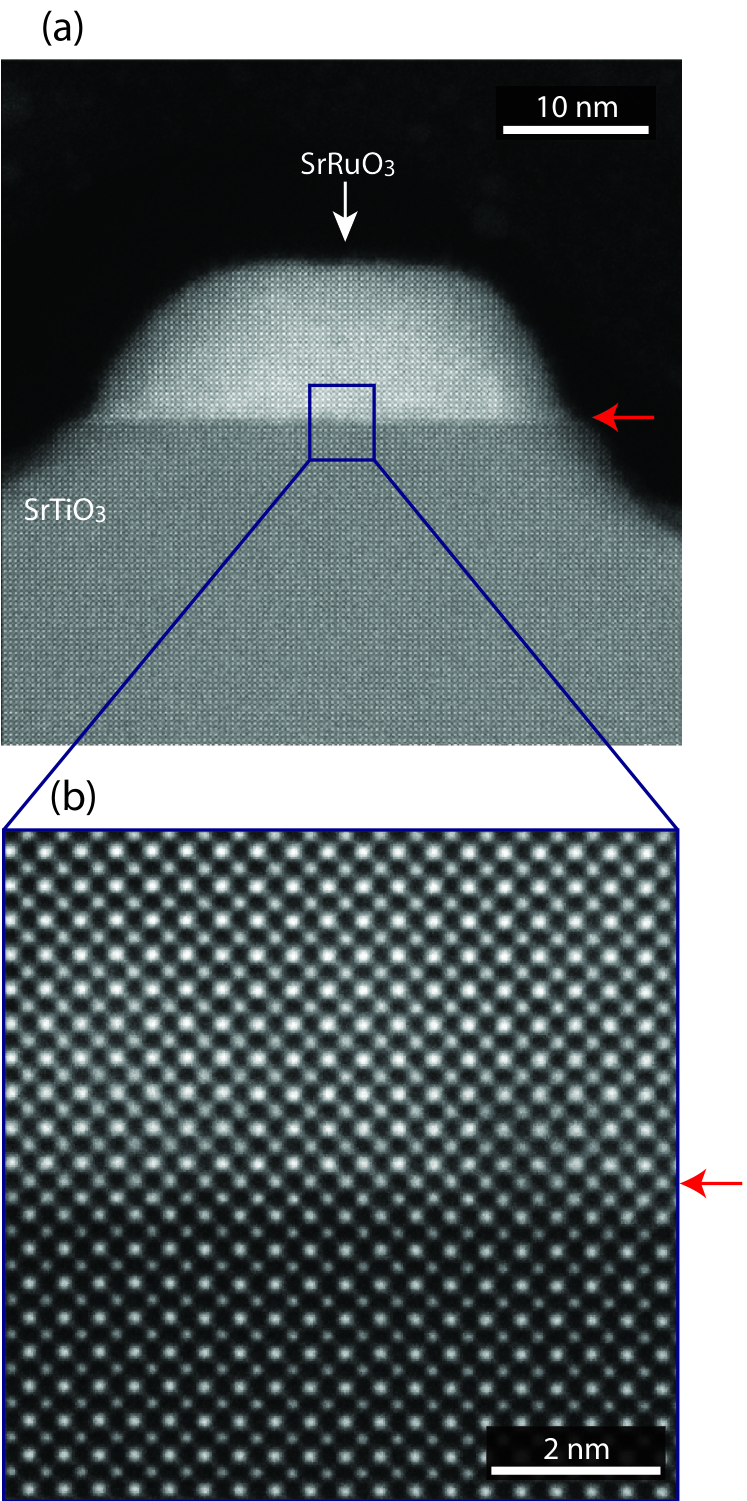
Figures 1 and 2 give an overview of the dots’ microscopic properties. Figure 1(b) is a scanning electron microscopy (SEM) image of a sample with a rectangular array of 20-nm SrRuO3 dots. A Z-contrast STEM image of a single-dot cross section from a different sample is shown in Fig. 2(a), which depicts a clear contrast between the SrRuO3 and the substrate material with a sharp interface. This is magnified in Fig. 2(b). During the sample preparation for TEM, the dot was cut through its center with a lamella thickness of nm. Therefore, the cross section shown in Fig. 2(a) provides a projection through almost the entire dot. The curved shape of the substrate near the dot and the shape of the dot itself are caused by non-uniform removal of material during dry etching with Ar ions.
The magnetic properties of different samples were measured using a SQUID magnetometer (Quantum Design MPMS) equipped with the reciprocating sample option (RSO) head. For all samples, the thickness of the SrRuO3 film equaled 12 nm (i.e., 32 unit cells of SrRuO3). Every sample was measured twice at different steps of the fabrication process: directly after the thin-film growth and then after being patterned into nanodots. To measure the zero-field-cooled and the field-cooled behavior of the magnetization, the samples were cooled to 4 K in zero magnetic field, after which an out-of-plane magnetic field of 0.1 T was applied. The samples were then warmed to room temperature and cooled again.
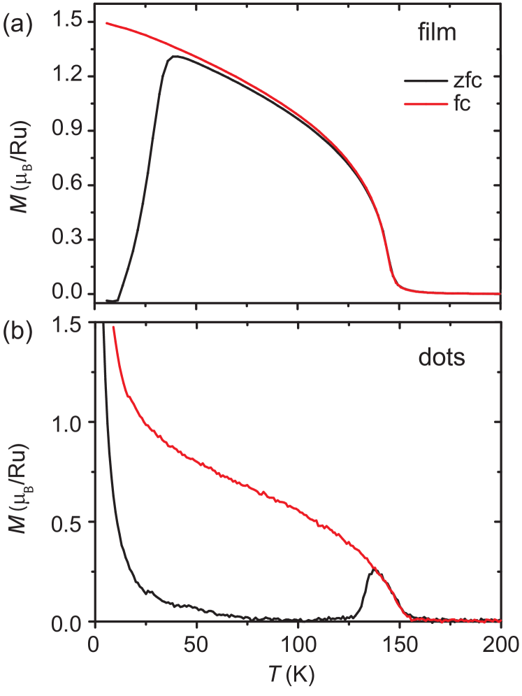
A typical characteristic of the temperature-dependent magnetization of a SrRuO3 film is shown in Fig. 3(a). The shape of the curve and the saturation magnetization of 1.5 B/Ru are in good agreement with the literature data Tian et al. (2007); Grutter et al. (2010). The Curie temperature TC is determined by the linear extrapolation of the transition curve to , although a finite magnetic moment exists above this temperature, attributed to the domain structure and film reorientation Xia et al. (2009). For all films, the transition has been found at a TC = 1491 K, which is comparable to the TC values reported in the literature for equally thick films deposited by pulsed laser deposition Bern et al. (2013); Chang et al. (2009). Fig. 3(b) shows an example of the magnetic transition curve for a patterned sample with a dot diameter of 20 nm. Considerably different is the behavior of the magnetic response at low temperatures, where a significant increase of the magnetization is observed. This is due to the paramagnetism inherent in SrTiO3 Coey, Venkatesan, and Stamenov (2016), which causes difficulties for measuring the dot magnetization because of the very small SrRuO3 volume compared to the SrTiO3 substrate. However, this contributes only to the low-temperature properties and does not affect the magnetization close to the ferromagnetic transition region, in which we are primarily interested here.
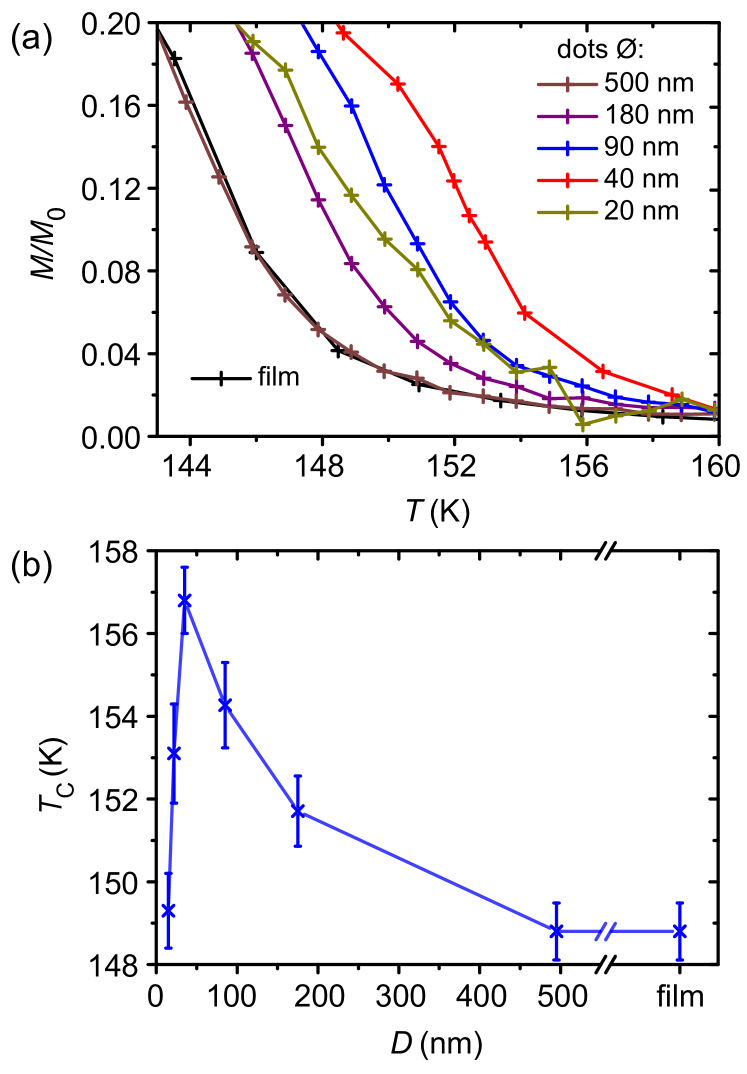
After patterning, the sample remains ferromagnetic with a TC = 153 K, i.e., 4 K higher than that of the film. This increase of the Curie temperature is systematically observed for dots of different sizes. To clarify this effect in more detail, a series of samples with different dot sizes (from 500 to 15 nm) was fabricated. The initial film morphology and their magnetic properties were similar. With decreasing dot size, the distance between them was scaled proportionally to keep the total amount of SrRuO3 constant. After patterning, the temperature dependence of the magnetization was measured for all samples using the procedure described above. The results of the measurements for dots of different sizes are depicted in Fig. 4(a) and the extracted variation of the Curie temperature in Fig. 4(b). The TC does not change after patterning for dots equal to or larger than 500 nm. For smaller dots, a gradual increase of TC with decreasing dot size is observed. This is valid down to a dot size of approximately 30 nm, after which TC starts to decrease, presumably due to surface defects and dead layers. A decrease of TC with shrinking feature size is well known for thin films Chang et al. (2009); Himpsel et al. (1998) and has been observed in nanoparticles of other perovskites Vasseur et al. (2006) and also for metals Rong et al. (2006). This reduction of TC is generally attributed to the reduced number of neighbors and the corresponding destabilization of the magnetic ordering Rong et al. (2006). Even for the smallest dot sizes, however, the Curie temperature exceeds that of the unstructured film.
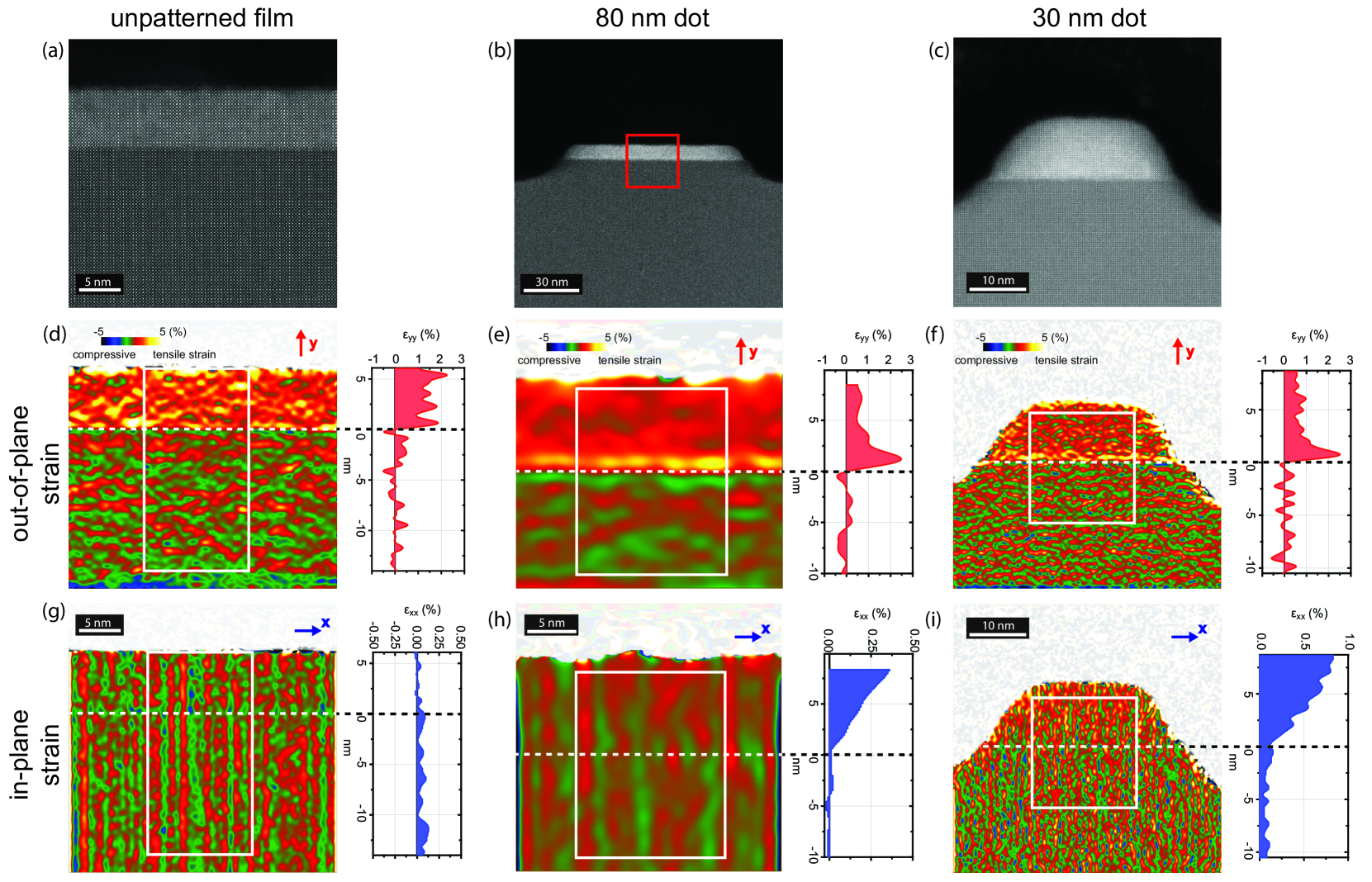
Strain is one of the mechanisms known to influence magnetic properties of SrRuO3. Using ab-initio density functional theory (DFT) calculations, it was shown in Ref. 29 that uniaxial and epitaxial strain in SrRuO3 significantly alters its magnetic properties. Experimental studies of SrRuO3 grown on different substrates Lu et al. (2015) demonstrate that the magnetic properties differ depending on the amount of strain in the film. Furthermore, SrRuO3 films released from their substrates demonstrate a 10 K higher TC of 160 K Gan et al. (1998). A different study Thomas et al. (2017) showed that a SrTiO3 capping layer grown on SrRuO3 epitaxial films deposited on DyScO3 modifies the oxygen octahedral structure in the SrRuO3 with a corresponding increase of the Curie temperature. To explore whether strain relief is responsible for the TC increase in our dot structures, we studied the strain in the dots by STEM. We used geometric phase analysis to analyze high spatial resolution STEM images in the in-plane and out-of-plane directions Hytch, Snoeck, and Kilaas (1998); Hytch, Purtaux, and Penisson (2003). The lattice constant of the SrTiO3 substrate was taken as a reference level. Fig. 5(d,g) shows the strain distribution of a SrRuO3 thin film grown on SrTiO3. The data reveals that the film is fully strained, i.e., the lattice constant in the in-plane direction remains unchanged across the interface (Fig. 5(g), right panel), whereas in the out-of-plane direction the unit cell of SrRuO3 is elongated by a constant value of 1.40.3 % compared to SrTiO3 (Fig. 5(d), right panel). These strain characteristics are altered by patterning the epitaxial film into nanodots, as shown by Fig. 5(e,h) for a 80-nm-diameter dot and Fig. 5(f,i) for a 30-nm-diameter dot. For both dot sizes, in the in-plane direction (Fig. 5(h,i)), starting from the interface, the lattice constant of SrRuO3 increases gradually, which indicates strain relaxation. For the 80-nm dot, the lattice constant has relaxed by 0.350.10 % at the top of the dot, whereas for the 30-nm dot the relaxation is even stronger. It reaches 0.750.10 %, matching fully relaxed SrRuO3. We link this lattice relaxation to the observed increase of the Curie temperature. In the out-of-plane direction (Fig. 5(e,f)) the behavior for dots of both sizes is similar. Here, in the first two unit cells close to the interface, we observed the strain close to that of the film, which, as expected, then decays together with the lateral strain relaxation to approach a three-dimensionally relaxed structure. A similar mechanism of patterning-induced strain relaxation has been observed before in patterned semiconductor nanostructures, for example Si Himcinschi et al. (2007), InGaN/GaN Ramesh et al. (2010) or (Ga, Mn)As Wenisch et al. (2007). We therefore conclude that the strain relaxation is responsible for the increase of the TC in these SrRuO3 nanodots.
IV Summary
In summary, using e-beam lithography of epitaxial SrRuO3 films, we have succeeded in fabricating nanosized dots of SrRuO3 ranging in size from several hundred nm down to 15 nm. SrRuO3 shows ferromagnetism even in the smallest dots. Unexpectedly, magnetometry reveals that the magnetic properties are enhanced for dot sizes below 500 nm, which manifests itself in an increase of the Curie temperature for small dots. We demonstrate that the Curie temperature depends on the size of the dots, increasing gradually from 149 K in the thin film and dots larger than 500 nm to 157 K at 30 nm dot size. This behavior is attributed to strain relaxation in the material caused by the removal of lateral constraint around the dot.
V Acknowledgements
GL acknowledges E. Goering (MPI for Intelligent Systems, dept. Modern Magnetic Systems) and E. Bruecher (MPI for Solid State Research, Chemical Service) for the support with magnetometry measurements. We thank T. Reindl, U. Waizmann and J. Weis for the technical support with sample fabrication. Discussions with J. Mydosh and M. Ternes are gratefully appreciated. HW gratefully acknowledges the China Scholarship Council (No. 201504910813) and the Max Planck Society for financial support. We thank Y. Wang, U. Salzberger, K. Hahn and P. Kopold for their support during TEM sample preparation and the TEM experiments. We acknowledge the assistance by B. Fenk for preparing FIB lamellas and by L. Jin from the Ernst Ruska-Centre Juelich for the nanomill preparation of TEM lamellas.
References
- Ashoori (1996) R. Ashoori, Nature 379, 413 (1996).
- Kastner (1993) M. Kastner, Phys. Today 46, 24 (1993).
- Bibes, Villegas, and Barthelemy (2011) M. Bibes, J. E. Villegas, and A. Barthelemy, Adv. Phys. 60, 5 (2011).
- Mannhart and Schlom (2010) J. Mannhart and D. G. Schlom, Science 327, 1607 (2010).
- Hwang et al. (2012) H. Hwang, Y. Iwasa, M. Kawasaki, B. Keimer, N. Nagaosa, and Y. Tokura, Nat. Mater. 11, 103 (2012).
- Baiutti et al. (2015) F. Baiutti, G. Logvenov, G. Gregori, G. Cristiani, Y. Wang, W. Sigle, P. A. van Aken, and J. Maier, Nat. Commun. 6, 8586 (2015).
- Yoshimatsu et al. (2011) K. Yoshimatsu, K. Horiba, H. Kumigashira, T. Yoshida, A. Fujimori, and M. Oshima, Science 333, 319 (2011).
- Bern et al. (2013) F. Bern, M. Ziese, A. Setzer, E. Pippel, D. Hesse, and I. Vrejoiu, J. Phys.: Condens. Matter 25, 496003 (2013).
- Mannhart et al. (2016) J. Mannhart, H. Boschker, T. Kopp, and R. Valenti, Rep. Prog. Phys. 79, 084508 (2016).
- Cen et al. (2009) C. Cen, S. Thiel, J. Mannhart, and J. Levy, Science 323, 1026 (2009).
- Cheng et al. (2011) G. Cheng, P. F. Siles, F. Bi, C. Cen, D. F. Bogorin, C. W. Bark, C. M. Folkman, J.-W. Park, C.-B. Eom, G. Medeiros-Ribeiro, and J. Levy, Nat. Nanotechnol. 6, 343 (2011).
- Ruzmetov et al. (2005) D. Ruzmetov, Y. Seo, L. J. Belenky, D.-M. Kim, X. Ke, H. Sun, V. Chandrasekhar, C.-B. Eom, M. S. Rzchowski, and X. Pan, Adv. Mater. 17, 2869 (2005).
- Landau, Reiner, and Klein (2012) L. Landau, J. W. Reiner, and L. Klein, J. Appl. Phys. 111, 07B901 (2012).
- Katine et al. (2003) J. Katine, M. Ho, Y. Ju, and C. Rettner, Appl. Phys. Lett. 83, 401 (2003).
- Koster et al. (2012) G. Koster, L. Klein, W. Siemons, G. Rijnders, J. S. Dodge, C.-B. Eom, D. H. A. Blank, and M. R. Beasley, Rev. Mod. Phys. 84, 253 (2012).
- Ishigami et al. (2015) K. Ishigami, K. Yoshimatsu, D. Toyota, M. Takizawa, T. Yoshida, G. Shibata, T. Harano, Y. Takahashi, T. Kadono, V. K. Verma, V. R. Singh, Y. Takeda, T. Okane, Y. Saitoh, H. Yamagami, T. Koide, M. Oshima, H. Kumigashira, and A. Fujimori, Phys. Rev. B 92, 064402 (2015).
- Chang et al. (2009) Y. J. Chang, C. H. Kim, S.-H. Phark, Y. S. Kim, J. Yu, and T. W. Noh, Phys. Rev. Lett. 103, 057201 (2009).
- Siemons et al. (2007) W. Siemons, G. Koster, A. Vailionis, H. Yamamoto, D. H. A. Blank, and M. R. Beasley, Phys. Rev. B 76, 075126 (2007).
- Lu et al. (2015) W. Lu, W. Song, P. Yang, J. Ding, G. M. Chow, and J. Chen, Sci. Rep. 5, 10245 (2015).
- Thomas et al. (2017) S. Thomas, B. Kuiper, J. Hu, J. Smit, Z. Liao, Z. Zhong, G. Rijnders, A. Vailionis, R. Wu, G. Koster, and J. Xia, Phys. Rev. Lett. 119, 177203 (2017).
- Jäger et al. (2018) M. Jäger, A. Teker, J. Mannhart, and W. Braun, Appl. Phys. Lett. 112, 116601 (2018).
- Tian et al. (2007) W. Tian, J. H. Haeni, D. G. Schlom, E. Hutchinson, B. L. Sheu, M. M. Rosario, P. Schiffer, Y. Liu, M. A. Zurbuchen, and X. Q. Pan, Appl. Phys. Lett. 90, 022507 (2007).
- Grutter et al. (2010) A. Grutter, F. Wong, E. Arenholz, M. Liberati, A. Vailionis, and Y. Suzuki, Appl. Phys. Lett. 96, 082509 (2010).
- Xia et al. (2009) J. Xia, W. Siemons, G. Koster, M. R. Beasley, and A. Kapitulnik, Phys. Rev. B 79, 140407 (2009).
- Coey, Venkatesan, and Stamenov (2016) J. M. D. Coey, M. Venkatesan, and P. Stamenov, J. Phys.: Condens. Matter 28, 485001 (2016).
- Himpsel et al. (1998) F. J. Himpsel, J. E. Ortega, G. J. Mankey, and R. F. Willis, Adv. Phys. 47, 511 (1998).
- Vasseur et al. (2006) S. Vasseur, E. Duguet, J. Portier, G. Goglio, S. Mornet, E. Hadova, K. Knizek, M. Marysko, P. Veverka, and E. Pollert, J. Magn. Magn. Mater. 302, 315 (2006).
- Rong et al. (2006) C. Rong, D. Li, V. Nandwana, N. Poudyal, Y. Ding, Z. L. Wang, H. Zeng, and J. P. Liu, Adv. Mater. 18, 2984 (2006).
- Zayak et al. (2008) A. T. Zayak, X. Huang, J. B. Neaton, and K. M. Rabe, Phys. Rev. B 77, 214410 (2008).
- Gan et al. (1998) Q. Gan, R. Rao, C. Eom, J. Garrett, and M. Lee, Appl. Phys. Lett. 72, 978 (1998).
- Hytch, Snoeck, and Kilaas (1998) M. J. Hytch, E. Snoeck, and R. Kilaas, Ultramicroscopy 74, 131 (1998).
- Hytch, Purtaux, and Penisson (2003) M. J. Hytch, J.-L. Purtaux, and J.-M. Penisson, Nature 423, 270 (2003).
- Himcinschi et al. (2007) C. Himcinschi, R. Singh, I. Radu, A. P. Milenin, W. Erfurth, M. Reiche, U. Gösele, S. H. Christiansen, F. Muster, and M. Petzold, Appl. Phys. Lett. 90, 021902 (2007).
- Ramesh et al. (2010) V. Ramesh, A. Kikuchi, K. Kishino, M. Funato, and Y. Kawakami, J. Appl. Phys. 107, 114303 (2010).
- Wenisch et al. (2007) J. Wenisch, C. Gould, L. Ebel, J. Storz, K. Pappert, M. J. Schmidt, C. Kumpf, G. Schmidt, K. Brunner, and L. W. Molenkamp, Phys. Rev. Lett. 99, 077201 (2007).