Photoinduced Rashba spin to charge conversion via interfacial unoccupied state
Abstract
At interfaces with inversion symmetry breaking, Rashba effect couples the motion of electrons to their spin; as a result, spin – charge interconversion mechanism can occur. These interconversion mechanisms commonly exploit Rashba spin splitting at the Fermi level by spin pumping or spin torque ferromagnetic resonance. Here, we report evidence of significant photoinduced spin to charge conversion via Rashba spin splitting in an unoccupied state above the Fermi level at the Cu(111)/-Bi2O3 interface. We predict an average Rashba coefficient of at 1.98 eV above the Fermi level, by fully relativistic first – principles analysis of the interfacial electronic structure with spin orbit interaction. We find agreement with our observation of helicity dependent photoinduced spin to charge conversion excited at 1.96 eV at room temperature, with spin current generation of . The present letter shows evidence of efficient spin – charge conversion exploiting Rashba spin splitting at excited states, harvesting light energy without magnetic materials or external magnetic fields.
Rashba effect has provided fertile ground for basic research and innovative device proposals in condensed matter. Particularly attractive is the fact that in crystals lacking spatial inversion symmetry the induced spin orbit field couples to the electron’s magnetic moment. This spin orbit coupling (SOC) allows the conversion of spin current to transverse electrical charge, or vice versa, the conversion of unpolarized electrical current to spin polarization and diffusion as spin current. These mechanisms have been confirmed in a variety of systems lacking spatial inversion symmetry, opening the condensed matter sub-field of spin orbitronics Otani ; Manchon . Although, the first demonstration of spin – charge interconversion occurred in semiconductor bulk systems, the recent focus has been the lack of spatial inversion symmetry at metal/metal, metal/semiconductor, metal/oxide and oxide/oxide interfaces; as well as surface states in topological insulators Ando . Common techniques for exploring the spin – charge interconversion phenomena at interfaces are the spin pumping and spin transfer torque ferromagnetic resonance. These techniques allow studying the conversions at occupied states below the Fermi level. Arguably, the hybrization of states at interfaces of seemingly different material systems lead to a complex modified electronic structure with multiple Rashba SOC crossings below and above the Fermi level, and even topological points. This statement has been tested by evidence showing a significant modulation of SOC as the Fermi level is increased and new states are occupied Liang ; Herranz ; Kondou . However, feasibility of spin to charge conversion via Rashba spin splitting at unoccupied states has been elusive.
In this letter we show evidence of photoinduced spin to charge conversion via Rashba spin splitting of unoccupied states at the Cu(111)/-Bi2O3 interface. Recent reports showed the efficient spin - charge interconversion phenomena at the Cu(111)/-Bi2O3 interface by microwave photon spin pumping Tsai , acoustic spin pumping Mingran and magneto optical Kerr effect detection of current induced spin polarization Puebla ; Florent . The origin of the formation of the two dimensional gas (2DEG) with SOC at this interface between polycrystalline layers is an ongoing topic of debate. One leading hypothesis is the formation of 2DEG by interfacial charge transfer facilitated by the presence of a significant concentration of oxygen defects; hypothesis recently proposed as mechanism for the formation of 2DEG at the amorphous / crystalline perovskite oxide interfaces Li . We recently reported the properties of the two dimensional electron gas formation in the Cu(111)/-Bi2O3 interface with spin orbit coupling by spectroscopic ellipsometry Manuel . Polycrystalline interfaces have the advantage of reduced interfacial strain and higher carrier concentrations when compared with highly crystalline interfaces. Here, we performed density functional calculations of our Cu(111)/-Bi2O3 Suppl . Figure 1a shows the calculated layer-projected density of states (LDOS) at the Cu(111)/-Bi2O3 interface (dashed line zone) and its vicinity. At the interface, it is possible to observe a modification of the LDOS at both sides close to the interface, corresponding to Cu and Bi2O3 hybridization of Cu-O-Bi states due charge transfer. We sketched the calculated charge density of the electronic state of the Cu(111)/-Bi2O3 interface in figure 1b; where blue, red and purple spheres are Cu, O and Bi atoms, respectively; yellow clouds represent the Cu-O-Bi states.
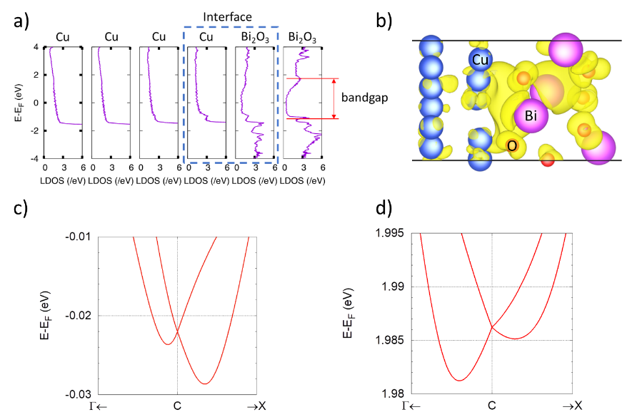
Band structure analysis around the C-point of states below the Fermi level, show a Rashba-like band splitting (see figure 1c). We evaluated Rashba parameters at C point (0.5, 0.5) in the unit of two-dimensional reciprocal lattice vectors. From the spin split energy band dispersion, the Rashba parameter is calculated by using an expression ER/kR, where ER is the Rashba energy and kR is the Rashba momentum offset Ishizaka . The averaged Rashba coefficient eV.m accounts for the energy band spin splitting around the Fermi energy as shown in Fig 1 (c), which is same order of magnitude of values reported by spin to charge conversion Mingran ; Tsai . Remarkably, around 1.98 eV above the Fermi level we locate another Rashba splitting of an unoccupied state. The averaged Rashba coefficient eV.m accounts for the large energy band spin splitting around 1.98 eV above the Fermi energy as shown in Fig 1 (d), almost two times larger than that observed around the Fermi level. The energy of this unoccupied state with Rashba splitting is in close proximity to the well-known interband transition between -states and -states of Cu, with both states participating at the interfacial hybrization.
We test the photoinduced Rashba spin to charge conversion with excitation energy of 1.96 eV at room temperature. The configuration of our photoinduced spin to charge conversion experiment is sketch in figure 2(a). We generate spin currents by the absorption of angular momentum from light, via the photovoltaic conversion. The angular momentum of light is dictated by its degree of circular polarization or helicity. Notice that, unlike standard heterostructures for photovoltaic devices where photovoltaic collection occurs at bottom and top electrodes, in our device the photovoltaic collection occurs in transverse geometry, following the inverse Edelstein effect (IEE) spin to charge conversion, E Mingran ; Tsai ; Rojas , where is the vector of spin polarization and is the flow direction of spin current. The interface is formed between a 30 nm thick Cu layer and 20 nm thick Bi2O3. These thicknesses are selected to suppress interaction of Si/SiO2 substrate and the excitation light. The laser beam has an incidence angle and an azimuthal angle . The photon polarization is controlled by a linear polarizer and a quarter wave plate mounted on a rotator.
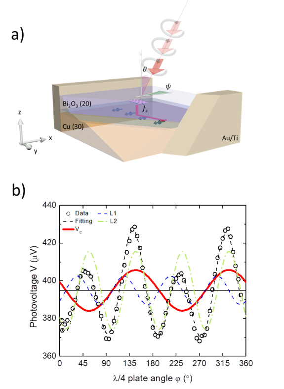
In figure 2(b), we show the helicity dependent photovoltaic measurement obtained with excitation laser energy of 1.96eV. Changing contributions of polarized light due to the rotation of the quarter wave plate () leads to periodic modulation in photovoltage with a periodicity of 90∘. Photovoltage peaks have different amplitudes, showing periodically two different values. This asymmetry comes from the circularly polarized light modulation analogous to the circular photogalvanic effect Ganichev . To better describe the contributions in our modulated signal, we fit the data with the following phenomenological formula Yuan ; Niesner .
| (1) |
Here, represents the amplitude associated with the degree of circular polarization of light or helicity (red solid line in Fig. 2), is the amplitude associated with the linear polarization of light (blue dash line in Fig. 2), depends on the Fresnel coefficients Okada (green dash line in Fig. 2) and is a non-modulated photovoltage offset. and are independent of light polarization. From the fitting we can obtain the amplitude of the photovoltage , which depends exclusively to the helicity of light, , and estimate the optical generated spin current by Mingran ; Rojas
| (2) |
Where is the inverse Edelstein effect length directly proportional to the Rashba parameter by ; is the momentum relaxation time governed by CuTsai ; is the width of our interface and is the sample resistance. We estimate the spin current by taking the voltage due to circular polarization from fitting of figure 2b, V, 10-9 m, 10 and giving a resistivity , we obtain 102, a value comparable with the spin current commonly generated by spin pumping experiments Mingran ; Rojas and previous reports of circular photovoltaic conversion by inverse spin Hall effect Isella ; Ando2 . This estimation is valid when the contribution from Schottky barrier is negligible. Such is the case for our Cu(111)/-Bi2O3 Suppl .
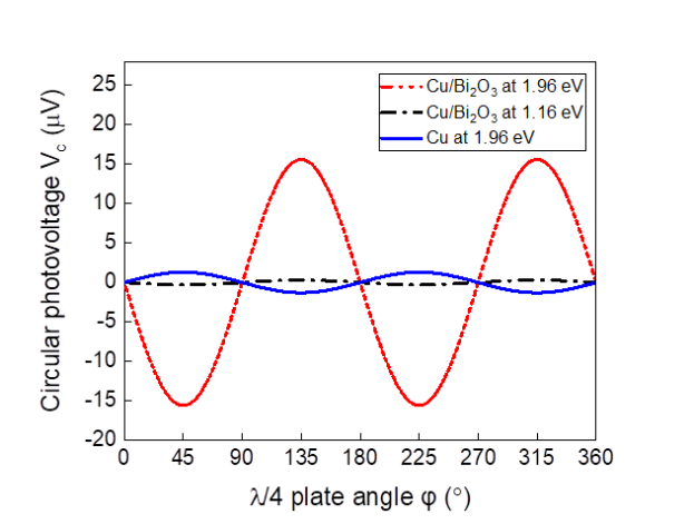
In further scrutiny figure 3 compares generation in three scenarios: excitation of Cu(111)/-Bi2O3 by 1.96eV (red dash line), 1.16eV (black dash-dot line) energy lasers and excitation of only Cu layer at 1.96eV (blue solid line), at ∘ and ∘. Figure 3 shows that (1.96eV) (1.16eV) for Cu(111)/-Bi2O3, indicating drastic suppression of the detected photovoltage coming from the circular polarization of light at 1.16eV, and also showing negligible contribution of circular polarized photovoltage coming from Si substrate, which has a band gap of 1.10eV. We also observe that (Cu(111)/-Bi2O3) (Cu(111)) with excitation at 1.96eV, indicating the relevance of the Cu(111)/-Bi2O3 interface. Moreover, we observe an opposite phase of spin to charge conversion for Cu(111)/-Bi2O3 and Cu(111), in agreement with the opposite sign of spin to charge conversion between Cu(111)/-Bi2O3 Tsai ; Mingran ; Puebla and the recent reports of conversion of the natural oxide in Cu An .
First-principle calculations showed hybrization of Cu-O-Bi charge states at our interface and Rashba splitting around 1.98eV above the Fermi energy, allowing the interfacial charge separation mechanism and IEE spin to charge conversion. Transverse photovoltage induced by circular polarized light can be also generated in surface state polaritons via an asymmetric variation of the photon drag effect Hatano ; Bliokh . This mechanism requires only surface state plasmons in metals and not necessarily the assistance of a semiconductor such as plasmon induced hot electrons mechanism Tatsuma ; Clavero . We tested the response of a Cu (111) layer to circular polarized light at 1.96eV. While the Cu (111) preserved the optical absorption due to Shockley surface states, we do not observe significant transverse photovoltage related to circular polarized light. Therefore, furthering suggesting combination of interfacial induced charge transfer and IEE as the origin for our circular polarized photovoltage at the Cu(111)/-Bi2O3 interface.
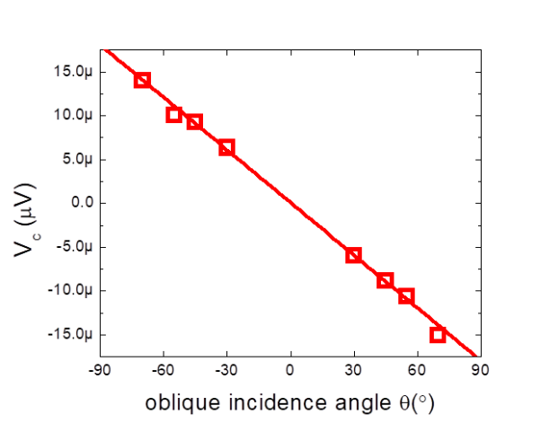
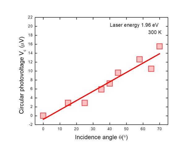
Finally we study the oblique incidence angle dependence of our photoinduced spin to charge conversion (see Fig. 4). The oblique incidence dependence shows an increase of circular photovoltaic signal as the projection is increase onto the plane, and reverses its sign at opposite oblique incidence angles, following spin to charge conversion mechanisms. The interpretation of our data works under the assumption of a interband transition of the -states to the partially filled -states of Cu, as suggested by the typical interband optical absorption, the hybrization of our first principles analysis and the prediction of a Rashba splitting of states at 1.98eV above the Fermi level.
To summarize, we showed the spin photovoltaic conversion at Cu(111)/-Bi2O3 interface. Due to the increasing number of interfaces with broken spatial inversion symmetry Ando ; Mingran ; Tsai ; Puebla ; Florent ; Li , we expect that the present work motivates further studies, advancing conversion efficiencies and understanding towards spin orbitronics in photovoltaics Amnu . From our present and previous reports, we have indication of spin to charge conversion at Cu(111)/-Bi2O3 interface due to Rashba spin orbit coupling Mingran ; Tsai ; Puebla ; Florent ; Rojas . Rashba spin orbit coupling is suggested as key component to suppress carrier recombination and enhanced carrier lifetime in perovskites Even ; Zheng . We observed an efficient photovoltaic conversion arising from a charge transfer mechanism at our Cu(111)/-Bi2O3 interface and Rashba spin splitting in an excited state. The photoinduced spin to charge conversion via Rashba spin splitting in an excited state motivates further studies in similar structures, and further understanding of the mechanism involved. Very recently, a related report shows circular photovoltaic signal at metal/metal interface Hirose , the interpretation of our results may shed new light in the understanding of this recent report and motive further studies. Our device is compatible with complementary metal-oxide-semiconductor (CMOS) technology, opening a new venue for exploring spin orbitronics at interfaces towards spin electronic devices beyond the Moore’s law Intel .
We acknowledge Naoki Ogawa and Kouta Kondo for fruitful discussions. This work was supported by Grant-in-Aid for Scientific Research on Innovative Area, Nano Spin Conversion Science (Grant No. 26103002 and No. 17H05180) and RIKEN Incentive Research Project Grant No. FY2016. The first-principles calculation was supported in part by MEXT as a social and scientific priority issue (Creation of new functional devices and high-performance materials to support next-generation industries) to be tackled by using post-K computer (Project ID: hp180206). F.A. was supported by the Ministry of Education, Culture, Sports, Science and Technology (MEXT) Scholarship, Japan
References
- (1) Y. Otani, M. Shiraishi, A. Oiwa, E. Saitoh and S. Murakami, Spin conversion on the nanoscale, Nature Physics 13, 829-832 (2017)
- (2) A. Manchon, et al., New prespectives for Rashba spin-orbit coupling, Nat. Mater. 14, 871-882 (2015)
- (3) Y. Ando and M. Shiraishi, Spin to Charge Interconversion Phenomena in the Interface and Surface States, J. Phys. Soc. Jpn. 86, 011001 (2017)
- (4) H. Liang, L. Cheng, L. Wei, Z. Luo, G. Yu, Ch. Zeng and Z. Zhang, Nonmonotonically tunable Rashba spin-orbit coupling by multiple-band filling control in SrTiO3-based interfacial d-electron gases, Phys. Rev. B 92, 075309 (2015)
- (5) G. Herranz, G. Singh, N. Bergeal, A. Jouan, J. Lesueur, J. Gázquez, M. Varela, M. Scigaj, N. Dix, F. Sánchez and J. Fontcuberta, Engineering two-dimensional superconductivity and Rashba spin–orbit coupling in LaAlO3/SrTiO3 quantum wells by selective orbital occupancy, Nat. Comm. 6:6028 (2015)
- (6) K. Kondou, R. Yoshimi, A. Tsukazaki, Y. Fukuma, J. Matsuno, K. S. Takahashi, M. Kawasaki, Y. Tokura and Y. Otani, Fermi-level-dependent charge-to-spin current conversion by Dirac surface states of topological insulators, Nat. Phys. 12, 1027–1031 (2016)
- (7) H. Tsai, S. Karube, K. Kondou, N. Yamaguchi, F. Ishii, Y. Otani, Clear variation of spin splitting by changing electron distribution at non-magnetic metal/Bi2O3 interfaces, Scientific Reports 8:1, 5564 (2018)
- (8) M. Xu, J. Puebla, F. Auvray, B. Rana, K. Kondou and Y. Otani, Inverse Edelstein effect induced by magnon-phonon coupling, Phys. Rev. B 97, 180301(R) (2018)
- (9) J. Puebla, F. Auvray, M. Xu, B. Rana, A. Albouy, H. Tsai, K. Kondou, G. Tatara, and Y. Otani, Direct optical observation of spin accumulation at nonmagnetic metal/oxide interface, Appl. Phys. Lett. 111, 092402 (2017)
- (10) F. Auvray, J. Puebla, M. Xu, B. Rana, D. Hashizume, Y. Otani, Spin accumulation at nonmagnetic interface induced by direct Rashba-Edelstein effect, Journal of Materials Science: Materials in Electronics 29, 18, 15664–15670 (2018)
- (11) C. J. Li, Y. P. Hong, H. X. Xue, X. X. Wang, Y. Li, K. Liu, W. Jiang, M. Liu, L. He, R. F. Dou, C. M. Xiong and J. C. Nie, Formation of Two-dimensional Electron Gas at Amorphous/Crystalline Oxide Interfaces, Sci. Rep. 8:404 (2018)
- (12) J.M. Flores-Camacho, J. Puebla, F. Auvray, Y. Otani, R.E. Balderas-Navarro, Two-dimensional electron gas in the Cu/Bi2O3 interface detected by mid-infrared ellipsometry, arXiv:1901.08671 [cond-mat.mes-hall] (2019)
- (13) See supplemental material in appendix
- (14) K. Ishizaka, et al., Giant Rashba-type spin splitting in bulk BiTeI, Nature Materials,10, 521 (2011)
- (15) J. C. Rojas-Sanchez, L. Vila, G. Desfonds, S. Gambarelli, J. P. Attane, J. M. De Teresa, C. Magen, and A. Fert, Spin-to-charge conversion using Rashba coupling at the interface between non-magnetic materials, Nat. Commun. 4, 2944 (2013)
- (16) S.D. Ganichev and W. Prettl, Spin photocurrents in quantum wells, J. Phys.: Condens. Matter 15 R935–R983 (2013)
- (17) H. Yuan, et al., Generation and electric control of spin–valley-coupled circular photogalvanic current in WSe2, Nat. Nano. 9, 851857 (2014)
- (18) D. Niesner, et al., Structural fluctuations cause spin-split states in tetragonal (CH3NH3)PbI3 as evidenced by the circular photogalvanic effect, PNAS 115 (38), 9509-9514 (2018)
- (19) K.N. Okada, et al., Enhanced photogalvanic current in topological insulators via Fermi energy tuning, Phys. Rev. B 93, 081403(R) (2016)
- (20) G. Isella, et al., Photon energy dependence of photo-induced inverse spin-Hall effect in Pt/GaAs and Pt/Ge, Appl. Phys. Lett. 106, 232402 (2015)
- (21) K. Ando, et al., Photoinduced inverse spin-Hall effect: Conversion of light-polarization information into electric voltage, Appl. Phys. Lett. 96, 082502 (2010)
- (22) H. An, Y. Kageyama, Y. Kanno, N. Enishi and K. Ando, Spin–torque generator engineered by natural oxidation of Cu, Nature Comm. 7:13069 (2016)
- (23) T. Hatano, et al., Transverse Photovoltage Induced by Circularly Polarized Light, Phys. Rev. Lett. 103, 103906 (2009)
- (24) K.Y. Bliokh and F. Nori, Transverse spin of a surface polariton, Phys. Rev. A 85, 061801(R) (2012)
- (25) T. Tatsuma, H. Nishi, and T. Ishida, Plasmon-induced charge separation: chemistry and wide applications, Chem. Sci. 8, 3325 (2017)
- (26) C. Clavero, Plasmon-induced hot-electron generation at nanoparticle/metal-oxide interfaces for photovoltaic and photocatalytic devices, Nat. Photo. 8, 95-103 (2014)
- (27) K. Amnuyswata, P. Thanomngam, Roles of spin-orbit coupling in tetragonal hybrid halide perovskite for photovoltaics light-absorber, Materials Today: Proceedings Vol. 5, Issue 7, Part 1, 14857-14861 (2018)
- (28) J. Even, L. Pedesseau, J-M Jancu and C. Katan, Importance of Spin–Orbit Coupling in Hybrid Organic/Inorganic Perovskites for Photovoltaic Applications, J. Phys. Chem. Lett., 4 (17), 2999–3005 (2013)
- (29) F. Zheng, L. Z. Tan, S. Liu and A. M. Rappe, Rashba Spin–Orbit Coupling Enhanced Carrier Lifetime in CH3NH3PbI3, Nano Lett., 15 (12), pp 7794–7800 (2015)
- (30) H. Hirose, N. Ito, M. Kawaguchi, Y.C. Lau, M. Hayashi, Circular photogalvanic effect in Cu/Bi bilayers, Appl. Phys. Lett. 113, 222404 (2018)
- (31) S. Manipatruni, D.E. Nikonov, I.A.,Young, Beyond CMOS computing with spin and polarization, Nature Physics 14, 338–343 (2018)
- (32) T. Ozaki, Variationally optimized atomic orbitals for large-scale electronic structures, Phys. Rev. B 67, 155108 (2003)
- (33) T. Ozaki and H. Kino, Efficient projector expansion for the ab initio LCAO method, Phys. Rev. B 72, 045121 (2005)
- (34) J. Perdew, K. Burke and M. Ernzerhof, Generalized Gradient Approximation Made Simple, Phys. Rev. Lett. 77, 3865 (1996)
- (35) G. Theurich and N. A. Hill, Self-consistent treatment of spin-orbit coupling in solids using relativistic fully separable ab initio pseudopotentials, Phys. Rev. B 64, 073106 (2001)
- (36) T. Ozaki and H. Kino, Numerical atomic basis orbitals from H to Kr, Phys. Rev. B 69, 195113 (2005)
- (37) M. Otani and O. Sugino, First-principles calculations of charged surfaces and interfaces: A plane-wave nonrepeated slab approach, Phys. Rev. B 73, 115407 (2006)
- (38) T. Ohwaki, M. Otani, T. Ikeshoji and T. Ozaki, Large-scale first-principles molecular dynamics for electrochemical systems with O(N) methods, J. Chem. Phys. 136, 134101 (2012)
I Appedix
I.1 Methods
I.1.1 Device fabrication and experimental setup
Our samples consist of a Cu(30nm)/Bi2O3(20nm) bilayer prepared on a Si substrate with a 300nm thick SiO2 layer. The sample is patterned by using mask-less UV-Lithography. The resists consist of a primer (hexamethyl-disilazane) and AZ1500, both are coated at 4000 rpm for 45 seconds and baked respectively for 5min and 10min. Depositions are done in-situ using e-beam evaporation at a vacuum pressure of 510-5 Pa at a rate of 1 Å/s for Cu and 0.2 Å/s for Bi2O3. Two electrodes made of Au(150nm)/Ti(5nm), also deposited by e-beam evaporation, are added to measure the voltage generated by illuminating a laser beam onto the sample. The laser beam has an incidence angle and an azimuthal angle . Our light excitations are continuous wave lasers at energies of 1.16eV and 1.96 eV. The laser spots are adjusted to approximately 400m for all the lasers, and placed at the center of our sample surface to minimize the effect of thermal gradients. The photon polarization is controlled by a linear polarizer and a quarter wave plate mounted on a mechanical rotator. The voltage is detected by a lock-in amplifier in open circuit mode synced at 400 Hz with a mechanical chopper.
I.1.2 First-principles calculation (Computational details)
Our density functional calculations were performed using OpenMX code Ozaki ; Ozaki2 within the generalized gradient approximation Perdew . We used 16121 regular k-point mesh and the fully relativistic total angular momentum dependent pseudo-potentials taking spin-orbit interaction (SOI) into account Theu . We adopted norm-conserving pseudopotentials with an energy cutoff of 300 Ry for charge density including the 5d, 6s and 6p-states as valence states for Bi; 2s and 2p for O; 3s, 3p, 3d and 4s for Cu.
The numerical pseudo atomic orbitals Ozaki3 are used as follows: the numbers of the s-, p- and d-character orbitals are three, three and two, respectively; The cutoff radii of Bi, O, and Cu are 8.0, 5.0 and 6.0, respectively, in units of Bohr. The dipole-dipole interaction between slab models can be eliminated by the effective screening medium (ESM) method OtaniM ; Oh . A Rashba energy ER and a Rashba momentum kR were obtained from a difference in energy and a distance in momentum space, respectively between the band crossing point, that is, C point (0.5, 0.5) and the band bottom point.
I.2 Additional data fittings
I.2.1 Polarization dependent photovoltage of Cu and Cu/Bi2O3
In figure 3 of our main text we showed a comparison of circular polarization photovoltage for Cu/Bi2O3 excited by laser energy of 1.96eV, 1.16eV and Cu layer excited by laser energy of 1.96eV. The circular polarization photovoltage is extracted from fitting following eq. (1) of our main text. For completeness, here we provide full fitting plots of similar device under same conditions (figure 5).
For our present study the most relevant component is the photovoltage associated to the circular polarization of light (VC). Similar to our results in the main text, we find that the maximum circular polarization photovoltage occurs for Cu/Bi2O3 excited by laser energy of 1.96eV. We also observed that the sign for circular polarization photovoltage for Cu/Bi2O3 and Cu layer have opposite signs, suggesting opposite spin to charge photo-conversion, in agreement with previous reports of spin to charge conversion in natural oxide in Cu An .
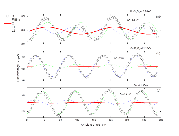
Additional to the circular polarization photovoltage VC, we also extract the two linear polarization photovoltage, L1 and L2. These two linear polarization components are spin independent, therefore out of the main scope of our present study. Nevertheless, we find appropriate to make some brief comments of our linear polarization photovoltages. In a general form, both the circular photovoltaic effect (VC in our manuscript) and linear photovoltaic effect (L1 and L2 in our manuscript) exist in non-centrosymmetric systems, meaning systems with spatial inversion symmetry breaking. While the circular photovoltaic effect is time reversal invariant, the linear photovoltaic effect is time reversal variant. Under homogeneous excitation and transverse geometry of incidence (the geometry of our experiments), there are two main sources of linear photovoltage: 1) the scattering of free carriers in phonons, defects and other carriers in noncentrosymmetric media (L1); and 2) The optical response and momentum transfer of s and p linear polarization, related to the Fresnel coefficients, as indicated in our manuscript (L2). Since the linear polarization is significantly affected by the refractive index of materials and the interaction of light with scattering centers, the presence or absence of a top Bi2O3 layer and changes of the excitation energy may significantly modify the linear polarization components L1 and L2, as we indeed observe in figure 5. For completeness, in figure 6 we provide an additional oblique incidence dependence plot of circular photovoltage excited at 1.96eV of a Cu/Bi2O3 device from a different batch to the data of figure 4 of our main text.
I.3 I-V characterization
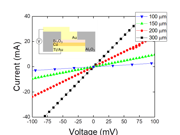
We measured I-V characteristics of our Cu/Bi2O3 heterojunction. I-V measurement indicates the formation of an Ohmic heterojunction, which minimize the influence of Schottky barrier rectification as mechanism of our photovoltaic conversion. I-V measurements were done using a stacking of top contact Ti(5nm)/Au(150nm), Cu(30nm)/Bi2O3(20nm), bottom contact Au(300nm), 200nm of Al2O3 were also deposited to avoid leakage current. Figure 7 shows I-V measurement with Ohmic junction behavior between Cu and Bi2O3 for samples with different contact area.
I.4 Optical absorption spectroscopy
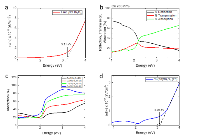
Optical absorption of Cu/Bi2O3 device by UV-Vis-NIR absorption spectroscopy (Shimadzu UV-3600 Plus) in the range from 0.9eV to 4eV, see figure 8. Figure 8a shows the Tauc plot of Bi2O3 (20nm) grown on sapphire (0001) showing a band gap at 3.21eV. Figure 8b shows the Transmission, Reflection and Absorption of Cu (30nm). Fig 8c shows the thickness dependence of Cu(X)/Bi2O3. The drastic change of absorption around 2eV corresponds to the interband transition from the 3d bands to the 4s band of Cu. Figure 8d shows the Tauc plot of Cu(30nm)/Bi2O3 showing a shift of band gap energy of Bi2O3 at 3.09 eV.
I.5 XRD spectroscopy
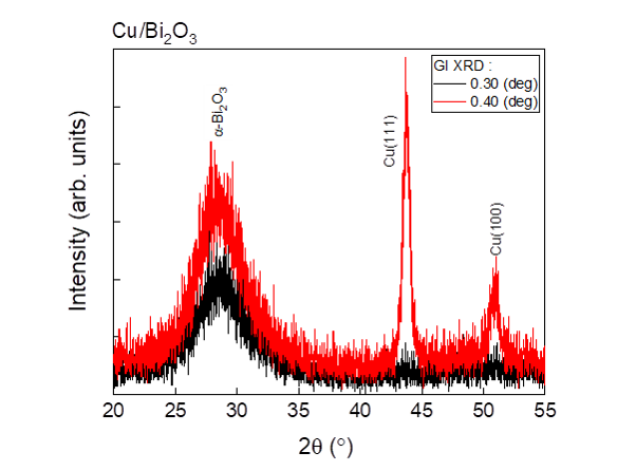
X-ray diffraction at grazing incident (GI) spectroscopy measurements were done for Cu/Bi2O3 with Rigaku SmartLab high resolution X-ray diffractometer (Fig.9). At an angle of 0.30∘, GI incidence (black line), only one feature appears, a broad peak at 28∘ at the interface of Cu/Bi2O3. This broad peak is the characteristic peak of our top Bi2O3 layer, and it indicates a amorphous structure in -phase, the most stable phase at room temperature for Bi2O3. At a GI angle of 0.40∘ (red line), the Cu layer shows preferential crystallinity at the interface in the (111) direction.