Cryogenic light detectors with enhanced performance for rare event physics
Abstract
We have developed and tested a new way of coupling bolometric light detectors to scintillating crystal bolometers based upon simply resting the light detector on the crystal surface, held in position only by gravity. This straightforward mounting results in three important improvements: (1) it decreases the amount of non-active materials needed to assemble the detector, (2) it substantially increases the light collection efficiency by minimizing the light losses induced by the mounting structure, and (3) it enhances the thermal signal induced in the light detector thanks to the extremely weak thermal link to the thermal bath.
We tested this new technique with a 16 cm2 Ge light detector with thermistor readout sitting on the surface of a large TeO2 bolometer. The light collection efficiency was increased by greater than 50% compared to previously tested alternative mountings. We obtained a baseline energy resolution on the light detector of 20 eV RMS that, together with increased light collection, enabled us to obtain the best vs discrimination ever obtained with massive TeO2 crystals. At the same time we achieved rise and decay times of 0.8 and 1.6 ms, respectively. This superb performance meets all of the requirements for the CUPID (CUORE Upgrade with Particle IDentification) experiment, which is a 1-ton scintillating bolometer follow up to CUORE.
keywords:
Double Beta Decay , Dark Matter , Scintillating bolometers , Cherenkov radiation , Particle identification methods , Cryogenic DetectorsPACS:
07.20.Mc , 07.57K.Kp , 23.40.-s , 29.40Ka , 29.40.Mc1 Introduction
The use of Low Temperature Detectors (LTDs) for sensing X-ray and -ray signals is quite widespread and well established [1]. LTDs are also widely used in the field of fundamental physics, especially for Double Beta Decay (DBD), and Dark Matter (DM) searches [2]. In these surveys the need for a hybrid detector, in which an energy release can be measured through different mechanisms, is of primary importance in order to distinguish the nature of interacting particles. For instance hybrid detectors can help identify and reject events caused by the natural background. With thermal detectors this can be achieved using scintillating or luminescent crystals. The simultaneous and independent readout of the heat and the (escaping) light produced by the interaction reveals the nature of the interacting particles thanks to the different scintillation yields of , and events. This discrimination technique is presently used for DM searches [3, 4, 5], DBD searches [6, 7, 8], and it can be also implemented for rare nuclear decays [9, 10, 11].
At milli-Kelvin temperatures, the light detectors are usually bolometers themselves: a dark thin crystal absorbs the photons, producing heat (phonons) that is measured by a suitable thermometer. The main difference among the various Bolometric Light Detector (BLD) instruments currently in use is the choice of the thermometer element, e.g. Transition Edge Sensors (TES) [12], Neutron Transmutation Doped (NTD) thermistors [13] or Micro Magnetic Calorimeters (MMC) [14].
The work presented here was performed within the CUPID framework [15, 16], the future follow up of CUORE [17] that represents the largest world-wide bolometric experiment to date. The aim was to develop NTD-based BLDs with improved performance in terms of sensitivity, time response and simplified packaging for large arrays. Using the tiny Cherenkov light emission of TeO2 [18, 19] to decrease by two order of magnitude the -induced background, requires a BLD with a S/N ratio of the order of 5 [16]: this corresponds to a RMS baseline resolution of the BLD of the order of 20 eV being the Cherenkov light signal of the order of 100 eV. Actually one can work towards the optimization of the light collection [20] and/or towards the energy resolution of the BLD or -as we made in this work- both. Additionally, in case of 100Mo-based compounds, beside the same need to suppress the surface -induced background, a fast time response of the BLD ( 1 ms) is mandatory to suppress the background induced the pile-up of the 2 DBD [21]: also in this case the S/N ratio will play an important role [22].
Our work has therefore focused on two aspects of BLD performance: (1) improving the response of the NTD thermometer and (2) increasing the light collection. While the first aspect is strictly related to a specific technique, the second aspect is worthy of additional remarks. The working principle of a BLD is irrespective of the sensor: a thin crystal wafer (usually Si or Ge) absorbs the emitted photons and converts them into heat. Unlike a conventional bolometric approach, we have to avoid the optical coupling between crystal and BLD made with optical grease or similar substance since the unavoidable heat flow through the optical coupling and the increase of the heat capacity of the system would reduce the independence of the two detectors, eliminating the possibility of particle discrimination afforded by the different scintillation yields. Therefore the thermal contact between the luminescent crystal and BLD has to be avoided, especially in the case of extremely low scintillation yields. This is true for most of the Mo-based compounds [7] and, even more importantly in case of Cherenkov signals. A 2615 keV -ray energy release in a CUORE-like TeO2 absorber produces a light signal in the BLD on the order of 100 eV [20]. For this reason the BLD is always facing the scintillating crystal without directly contacting it via a coupling medium.
In the following section it is shown that if the BLD is simply resting on the crystal surface, held in position only by gravity, the thermal coupling between the BLD and the crystal is almost negligible and the leakage of the BLD thermal signal through the scintillating crystal vanishes. This fact can be explained considering the acoustic mismatch described in the diffused mismatch model whereby the heat carriers (phonons) in insulating materials are scattered at the interfaces [23, 24]. This approach shows that the thermal resistance between two dielectric crystals is strongly dependent on the surface state, on the different phonon characteristics in the two materials (density and Debye temperature), and on the applied force. This latter parameter has a significant effect. When two solids are placed in contact with each other, the actual contact area can be much smaller than the cross sections involved due to surface irregularities. By rising the applied force between the materials, a plastic or permanent deformation occurs and the ”real” contact surface area increases. The result of this action is that the thermal conductance of the contact is directly proportional to the applied force [25, 26].
Although such simple stand will clearly not produce a so-called ”optical matching,” the light collection will be definitively larger due to geometrical factors 111For instance if the BLD is held in its own structure, depending on the mounting scheme, there are generally a few mm of distance from the BLD to the scintillating crystal. This increases the chance for photon escape or absorption by the holding structure rather than the BLD.. In addition, removing the BLD mounting structure decreases the presence of materials and surfaces close to the detector which reduces possible radioactive contamination, a fundamental aspect of dealing with rare event searches.
2 Bolometric Light Detectors
Our BLDs are usually constituted by electronic grade undoped Ge wafers, coupled with Ge NTD thermistors. We started to develop these detectors coupled with several scintillating DBD crystals [27] and we deeply characterized their operation and performances [28] to finally realize the LUCIFER [29] experiment, which has been renamed CUPID-0 [30].
Each BLD of CUPID-0 (totalling 26 detectors) was made by a double side polished electronic grade undoped Ge wafer (44.5 mm diameter, 0.17 mm thick). The NTD thermistor, with dimension of (2.85 2 0.5) mm3, is glued through six small glue dots ( 0.5 mm diameter, 0.05 mm height) made with Araldit® Rapid glue. The performance of six of these detectors was evaluated in a dedicated test run [31] and the results are summarized in Tab. 1.
To further optimize our BLDs, we produced a set of devices based on the pioneering work of Coron et.al. [32]. For this study we (1) decreased the heat capacity (size) of the thermistor, (2) increased the thermal conductance between the thermistor and the Ge wafer, and (3) decreased the thermal conductance to the thermal bath. With respect to the thermistor size, we used thermistors with a dimension of (2.85 1 0.4) mm3, roughly 2.5 times smaller than the CUPID-0 devices. We also decided to replace the six glue dots with an uniform glue layer, thus increasing the thermal conductance between the thermistors and light-absorbing Ge wafer.
It should be noted that in our experience the use of glue dots instead of a more effective thin gluing layer is preferred when coupling inherently different materials (e.g. TeO2 crystals and Ge thermistors). The dot approach reduces the mechanical stresses induced by differential thermal contraction of the materials when cooled. In such cases, and especially when working with larger-sized thermistors, we sometimes observed cracks on the crystal surface after a cooling cycle. This phenomenon is greatly reduced in our case since we glue Germanium thermistors to Germanium light absorbers and use smaller thermistors. Even in this case, however, there are some small unavoidable stresses due to misorientation between the thermistor and absorber crystallographic planes, but we have found that these effects never led to visible cracks.
With respect to the mounting (i.e. the conductance to the thermal bath), there are many ways to hold the BLD in place. In earlier work we adopted two [28] or three [30] small PTFE clamps that squeeze the edge of the Ge, keeping it fixed in a Cu standalone holder. PTFE is a common material also used by other groups working with NTD sensors [33] and with MMC detectors [14]. Other clamping schemes and material choices have been demonstrated by the CRESST group. These include bronze clamps and Silicon or CaWO4-based sticks [34]. The design used in [32], however, is probably the most complex from a construction point of view, using several ultra thin superconductive wires to suspend the Ge wafer from a copper frame to produce a negligible thermal link that maximizes the heat flow from the wafer to the NTD.
| Rwork | Response | Baseline RMS | ||
| [M] | [V/keV] | [eV] | [ms] | [ms] |
| 0.87 | 1.36 | 43 | 1.77 | 5.06 |
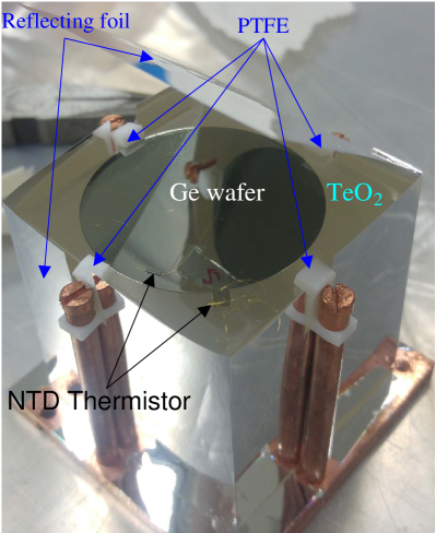
We decided to avoid any kind of holding structure whatsoever so we laid the BLD directly on the crystal, kept in position only by its weight (1.1 g). In this configuration the main thermal link between the BLD and the cryostat is represented by the thin gold NTD thermistor wires ( 2 15 mm length, 25 m diameter). As mentioned above, the expected thermal conductance to the scintillating crystal is negligible. The crystal chosen for this test was a (50.5 50.5 50.5) mm3 TeO2 crystal. The aim was to test the new setup with a light signal on the order of few tens of eV. The Ge light-absorbing wafer belongs to the batch used for CUPID-0, which include a 70 nm SiO anti-reflecting coating [35] that was deposited on the side that rests on the TeO2 crystal.
3 Experimental details
The TeO2 crystal was mounted in a similar way as described in [19, 36] with the only exception that the TeO2 crystal was standing on the reflecting foil and both TeO2 and BLD were not equipped with Si heaters. These heaters were normally glued on the bolometer to inject pulsed thermal signals for gain stabilization. The TeO2 face supporting the BLD and the opposite one were polished at (nearly) optical level. The remaining four lateral faces were matted in order to increase light collection [20].
The TeO2 crystal is held by four S-shaped PTFE supports that are fixed to Cu columns. The PTFE contracts upon cooling, creating a tensioned support that maintains the crystal position.
In order to maximize light collection, the crystal is completely surrounded by a plastic reflecting sheet (3M VikuitiTM), in the same way as in [19, 36]. A photograph of the detectors is presented in Fig. 1.
The entire setup was enclosed in a Cu box and thermally coupled to the mixing chamber of the CUPID R&D cryostat, a 3He/4He dilution refrigerator installed deep underground within Hall C of the Laboratori Nazionali del Gran Sasso, Italy. To avoid vibrations reaching the detectors, the box is mechanically decoupled from the cryostat by utilizing a two-stage pendulum system [37].
The thermistors of the detectors are biased with a quasi-constant current produced by applying a fixed voltage through large (27+27 or 2+2 G) load resistors [38]. When light is absorbed in the Ge wafer, a thermal pulse is produced which is subsequently transferred to the NTD sensor, changing the resistance of the thermistor. This, in turn, creates a voltage change across the current-biased NTD which is amplified using front end electronics located just outside the cryostat [39]. The signals are then filtered by an anti-aliasing 6-pole Bessel filter (with a cutoff frequency of 16 Hz for the TeO2 crystal and 550 Hz for the BLD) and finally fed into a NI PXI-6284 18-bit ADC.
The sampling rate of the ADC was 1 kHz for the TeO2 crystal and 8 kHz for the BLD.
The two independent triggers are software generated such that when a trigger fires, the
corresponding waveform is recorded. Moreover, when the trigger of the
TeO2 crystal fires, the corresponding waveform of the BLD is always
recorded, irrespective of its trigger. A detailed description of the DAQ system can
be found in [40].
The amplitude and the shape of the voltage pulses are then determined via off-line analysis.
The pulse amplitude of the thermal signals is estimated by the Optimum Filtering (OF)
technique [41, 42], that maximizes the signal-to-noise ratio
in a way that improves the energy resolution and lowers the threshold of the detector.
The amplitude of the light signal, however, is evaluated from the filtered waveform
at a fixed time delay with respect to the TeO2 bolometer, as described in detail
in [43].
The amplitude of the acquired TeO2 heat signals is energy-calibrated using several
-ray peaks from a 228Th source.
The BLD, on the contrary, is calibrated thanks to the 5.9 keV and 6.5 keV X-ray
quanta produced by a 55Fe X-ray source permanently faced to the detector.
4 Data analysis and results
4.1 BLD performance
The crystals were tested at a cryostat base temperature of 11 mK. In order to obtain a fast response, we operated the BLD in the so-called ”over-biased” configuration whereby the biasing current of the circuit is set much larger than the current that would ensure the highest absolute thermal response [13]. This choice ensures a small working resistance, thus minimizing the effect of the low pass filtering induced by the overall capacity (200 pF) of the front end readout wires.
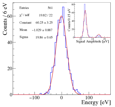
In Fig. 2 we show the 55Fe calibration spectrum obtained with the BLD. The baseline energy resolution (ie, the absolute sensitivity) of the BLD is given by the width of randomly acquired baselines (noise) after the application of OF. As is typical for this style of detectors, the energy resolution of monochromatic energy absorption events is much worse than the baseline resolution, irrespective of the type of sensor [13, 12].
The noise and signal power spectra of the BLD are presented in Fig. 3.
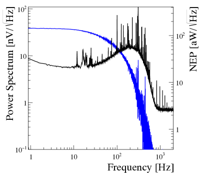
The bump that can be observed in Fig. 3 at 400 Hz arises from a resonance that enhances the thermal noise generated within the thermistor. This occurs when the impedance of the parasitic capacitance of the link becomes smaller than that of the thermistor, which is a fed-backed device [44]. The bump is found at the border of the bandwidth of the signal and is rejected from the optimum filter algorithm.
Fig. 4 shows the corresponding rise and decay times of 55Fe X-rays absorption events.
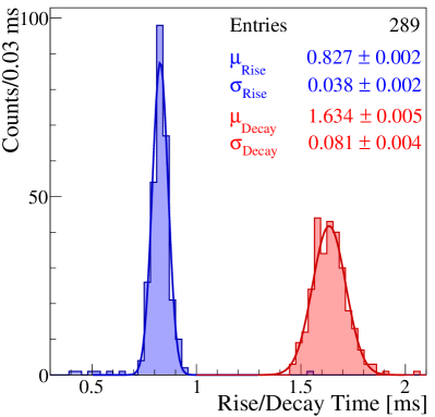
The measured rise time shown in Fig. 4 is most likely slower than the intrinsic rise time of the detector since it contains contributions from the Bessel filter (independent from the thermistor impedance) and from the capacitance of the readout wires. This last contribution is difficult to measure since it involves the dynamic resistance of the thermistor. The contribution of the 550 Hz Bessel filter to the rise time was evaluated in [13] and reported as 0.65 ms. Thus, after applying a quadratic deconvolution, the intrinsic rise time of our BLD should be of the order of 0.5 ms, compatible with the expectation of [32]. The overall performance of the BLD is summarized in Tab. 2.
| Rwork | Response | Baseline RMS | ||
| [M] | [V/keV] | [eV] | [ms] | [ms] |
| 1.47 | 3.86 | 20 | 0.83 | 1.63 |
4.2 Heat and Light measurement
In order to evaluate the long-term discriminatory performance of our BLD, we performed a 70 h run that included two event-generating calibration sources embedded into the setup. A 228Th source was placed a few cm away from the TeO2 crystal and a smeared 238U source was applied to the inside of the light reflector facing the TeO2. The aim of the source was to directly measure the discrimination capability between and in the DBD region of interest of 130Te. The source was made using 2 of a standard calibrated solution (0.1 %) of 238U, and the dried source deposition was covered with a 6 aluminized Mylar foil to smear the energy.
The light vs heat scatter plot is presented in Fig. 5 and shows an unexpected feature.
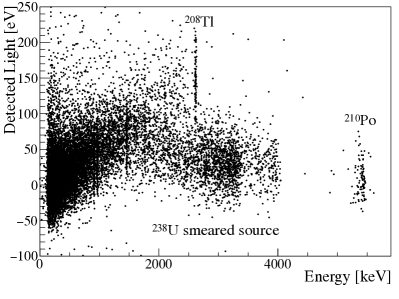
The 238U -events arising from the smeared source clearly show a tiny light emission that increases towards lower energies. This feature can only be ascribed to an energy loss in the Mylar which emits few scintillation photons. To avoid this effect we usually face the aluminized surface of the Mylar towards the crystal so as to reflect the (very few) photons that could be produced in this plastic. This time however, we mistakenly mounted the Mylar with the uncoated side towards the detector. This was confirmed after subsequently opening the cryostat and checking.
The result is shown in Fig. 5: the amount of Cherenkov light, produced by a 2615 keV , that is collected with this new set-up is (151 4) eV, 50 % larger with respect to all our previous measurements with massive crystals [20], as well as roughly 50 % larger with respect to a measurement recently performed with a NTD-based light detector [33] of the same type (considering the 40 % reduced transmission area between BLD and crystal, as declared in the article). The light distribution of the 74 events belonging to the internal 210Po at 5407 keV (5304 keV + 103 keV nucleus recoil) shows a mean value of (5.8 3.3) eV, still compatible with zero (see Sec. 5) as it should be if the light only arises from the Cherenkov effect. More importantly, the width of the light distribution of ’s is =(22.7 2.7) eV, fully compatible with the RMS noise of the BLD of Tab. 2. The light signal induced by the 2615 keV -on the contrary- shows a width of =(31.5 4.3) eV which is a result of the photostatistics and the light collection.
In order to evaluate the Discrimination Power (DP) that can be obtained between the and distributions at 2528 keV (the Qββ-value of the DBD of 130Te) we use the same formula and arguments used in [19, 33]: the DP can be quantified as the difference between the average values of the two distributions normalized to the square root of the quadratic sum of their widths:
| (1) |
Re-scaling the light signal from 2615 to 2528 keV, we obtain DP=3.6, using one highly likely assumption that an particle at 2528 keV will show a light signal equal than the same particle at 5304 keV (210Po). This DP is the best ever achieved with large mass TeO2 crystals (M 7 g) and without the need for additional Neganov-Luke amplification [33, 45, 46], or more sophisticated TES sensors [47] or both [48].
5 Thermal conductance
As stated in Sec. 1, the actual goal of this work was to experimentally demonstrate that the BLD can rest on the scintillating or luminescent crystal without heat sinking to it. Using the results in the previous section we can now calculate a limit on the heat flow through the Ge wafer and the TeO2. If one assumes that a 5407 keV energy release in the TeO2 produces a mean value BLD signal that only depends on the heat flow (assuming no light emission), then we have an upper limit for the ratio of the heat flow through TeO2 and Ge: 5.8 eV/5407 keV10-6.
In our case, an extremely low heat conductance was determined experimentally using static conditions. We measured the base resistance of the BLD as 223.5 M (corresponding to 11.8 mK), keeping the TeO2 thermistor unbiased (i.e. no power dissipation in it). We then gave the maximum (allowed by our biasing set-up) bias to the TeO2 thermistor, corresponding to 4.8 nA, and the TeO2 thermistor changed its resistance from 626 M (bias 0) to 1.71 M. The power dissipated on the TeO2 was therefore 40 pW. The base resistance of the BLD decreased to 222.8 M, which corresponds to a temperature increase of only 4.3 0.2 K. The same operation was performed with the BLD in working condition, i.e. bias current of 3.7 nA and a resistance of 1.47 M (corresponding to 23 mK), and no variation of the baseline of the BLD was registered. A further investigation of the thermal conductance between a Ge-BLD and a TeO2 crystal was performed by exploiting a small TeO2 crystal ( mm3, 34 g mass). We used a standard BLD, i.e., the same thickness and height as in the previous discussion, but with the Ge wafer held with PTFE clamps in a stand-alone Cu mounting [13]. For this experiment we rested the mm2 surface of the 34 g crystal on the Ge wafer. The NTD thermistor-equipped TeO2 crystal was surrounded with the same reflecting foil and we performed the same measurement described in Sec. 4.2 with the same overall setup. This time a 5304 keV 210Po decay occurring in the TeO2 created a mean signal in the BLD of (317 29) eV, definitively not compatible with the result of Sec. 4.2. The mean (light) signal registered in coincidence with the 2615 keV -line of 208Tl was (336 5) eV. The -induced signal in the BLD, therefore, has to be ascribed to an effective thermal transfer from the TeO2 to the BLD. We can make a very rough estimation of the size of this transfer using the results of the measurement of Sec. 4.2. If we assume the heat conductance to be linearly proportional to the pressure force between the two mediums, then we may simply compare the weight differences: 1.1 g in the case of the wafer resting onto the TeO2 crystal versus 34 g in this last configuration. Their ratio, i.e. 31, should be, in first approximation, the ratio between the thermal conductance in the two setups. Ascribing the signal of Sec. 4.2 exclusively to thermal transfer we would expect a thermal transfer signal of (180 90) eV, which is compatible with the 317 eV observed during this measurement. On the other hand, under the same assumption, we can evaluate the 2615-keV induced Cherenkov light signal of this crystal as the difference between the observed signal and the re-scaled thermal transfer evaluated from the . In this way we observe that the energy of the Cherenkov light emission in this 34 g crystal is (185 15) eV.
6 Conclusions
We have demonstrated the possibility of mounting BLDs by simply resting them on the surface of the corresponding scintillating crystal. With this new mounting method the light collection can increase up to 50% with respect to standard setups. We do not observe appreciable heat flow between the scintillating crystal and BLD. We also improved the time response of our thermistor-based light detectors, reaching a rise time of 0.8 ms and demonstrating that 0.5 ms is achievable. This time response is necessary to remove the background induced by the pile-up of the 2-DBD mode in the case of 100Mo-based crystals. We reached a baseline resolution of 20 eV RMS, more than 2 times better than the average value our previous CUPID-0-like detectors. Thanks to these developments, we definitively demonstrated that standard thermistor-based BLDs can be used for CUPID, both to read out the tiny Cherenkov light of TeO2 as well as to read out the Mo-based scintillating crystals.
We do believe that this simplified technique could be applied to any kind of BLD, irrespective of the sensor type. The first approximation thermal conductance between crystal and BLD does not depend upon the energy of the phonons, so we would expect that thermal transfer would be as negligible in TES or MMC devices as it is in our NTDs. More generally this new technique could be also applied in the case of stacked, standard small bolometers, provided that the weight does not exceed a few grams. However, since the measured thermal transfer is rather small, the weight of the bolometer will not be a significant limiting factor in low energy threshold applications.
7 Acknowledgments
This work was performed within the CUPID experiment founded by INFN and supported by the National Science Foundation under Grant NSF-PHY-1614611.
We thank the CUPID-0 and the CUORE collaborations for the overall support and for sharing their DAQ and software. We express our gratitude to LNGS for the generous hospitality and, in particular, to the mechanical workshop personnel including E. Tatananni, A. Rotilio, A. Corsi, and B. Romualdi for their continuous and constructive help. We are also grateful to M. Guetti for his invaluable support and expertise in the cryostat facility maintenance. We acknowledge Dr. C. Arnaboldi for his precious support, even though he has left this field of research many years ago. We are especially grateful to E. Ferri for her kind support in the thermistor wire-bonding.
References
- [1] J.N. Ullom, D.A. Bennet, Supercond. Sci. Technol. 28 (2015) 084003
- [2] S. Pirro, P. Mauskopf, Annu. Rev. Nucl. Part. Sci. 67 (2017) 161
- [3] G. Angloher, et al., Eur. Phys. J. C 76 (2016) 25
- [4] G. Angloher et al., JINST 12 (2017) P11007
- [5] G. Angloher et al., Astropart. Phys. 84 (2016) 70
- [6] O. Azzolini, et al., Phys. Rev. Lett. 120 (2018) 232502
- [7] E. Armengaud, et al., Eur. Phys. J. C 77 (2017) 785
- [8] G.B. Kim, et al., Astropart. Phys. 91 (2017) 105
- [9] P. de Marcillac, et al., Nature 422 (2003) 876
- [10] N. Casali, et al., Journal of Physics G 41 (2014) 075101
- [11] L. Pattavina, et al., Eur. Phys. J. A 54 (2018) 79
- [12] J. Rothe, et al., J. Low Temp. Phys. 193 (2018) 1160
- [13] J.W. Beeman, et al., JINST 8 (2013) P07021
- [14] H.J. Lee, et al., Nucl. Instr. and Meth. 784 (2015) 508
- [15] D.R. Artusa, et al., Eur. Phys. J. C 74 (10) (2014) 1
- [16] The CUPID Group of Interest, arXiv:1504.03612 [physics.ins-det]
- [17] CUORE Coll.: C. Alduino, et al., Phys. Rev. Lett. 120 (2018) 132501
- [18] T. Tabarelli de Fatis, Eur. Phys. J. C 65 (2010) 359
- [19] D.R. Artusa, et al., Phys. Lett. B 767 (2017) 321
- [20] N. Casali, Astropart. Phys. 91 (2017) 44
- [21] D.M. Chernyak, et al., Eur. Phys. J. C 72 (2012) 1989
- [22] D.M. Chernyak, et al., Eur. Phys. J. C 77 (2017) 3
- [23] D.S. Matsumoto , et al., Phys. Rev. B 16 3303 (1977) 3303
- [24] E.T. Swartz, R.O. Pohl, Rev. Mod. Phys. 61, 605 (1989)
- [25] M. Barucci, et al., J. Low Temp. Phys. 123 (2001) 303
- [26] G. Ventura, L. Risegari, in The Art of Cryogenics ISBN: 9780080444796 Elsevier, 2008 pp 89-102
- [27] S. Pirro, et al., Phys. Atom. Nucl.69 (2006) 2109
- [28] J.W. Beeman, et al., J. of Instr. 8 (2013) P07021
- [29] J.W. Beeman, et al., Adv. in High Energy Phys. (2013) 237973
- [30] O. Azzolini, et al., Eur. Phys. J. C 78 (2018) 428
- [31] D.R. Artusa, et al., Eur. Phys. J. C 76 (2016) 364
- [32] N. Coron, et al., Optical Engineering, 43 No. 7 (2004) 1568
- [33] L. Bergé, et al., Phys. Rev. C 97 (2018) 032501
- [34] R. Strauss, et al., Nuc. Instr. Meth. A 845 (2017) 414
- [35] M. Mancuso, et al., EPJ Web of Conferences 65 (2014) 04003
- [36] N. Casali, et al., Eur. Phys. J. C (2015) 75: 12
- [37] S. Pirro, Nucl. Instrum. Methods A 559 (2006) 672
- [38] C. Arnaboldi, et al., IEEE Trans. on Nucl. Science 49 (2002) 1808
- [39] C. Arnaboldi, et al., Nucl. Instrum. Meth. A 520 (2004) 578
- [40] S. Di Domizio et al., JINST 12 (2018) P12003
- [41] E. Gatti, P. Manfredi, Riv. Nuovo Cimento 9 (1986) 1
- [42] C. Alduino, et al., Phys. Rev. C 93 (2016) 045503
- [43] G. Piperno, S. Pirro, M. Vignati, JINST 6 (2011) P10005
- [44] C. Arnaboldi, et al., IEEE Transaction on Nuclear Science 52(2005) 1630
- [45] L. Pattavina et al., J. Low. Temp. Phys. 184 (2016) no.1-2, 286
- [46] L. Gironi et al., Phys. Rev. C 94 (2016) 054608
- [47] K. Schäffner, et al., Astropart. Phys. 69 (2015) 30
- [48] M. Willers, et al., J. of Instr. 10 (2015) P03003