Shape effect on the valley splitting in lead selenide nanowires
Abstract
We study the cross-section shape and size effects on the valley splitting in PbSe nanowires within the framework of empirical tight-binding method. We consider ideallized prismatic nanowires, grown along [110], with the cross-section shape varying from rectangular (terminated by and facets) to rhombic (terminated mostly by facets). The valley splitting energies have the maximal value (up to hundreds meV) in rectangular nanowires, while in rhombic ones they are almost absent. The shape dependence is shown to be similar for a wide range cross-section sizes and different point symmetries of nanowires.
I Introduction
Lead chalcogenide nanowires (NWs) have a wide range of possible applications. They can be used as circuit components Talapin and Murray (2005); Kim et al. (2011), light emitting (detecting) Sukhovatkin et al. (2009); Padilha et al. (2010) and energy harvesting Gesuele et al. (2012); Davis et al. (2015) devices. Throughout the past decades a big effort has been made towards experimental NW growth techniques Lifshitz et al. (2003); Cho et al. (2005); Fardy et al. (2007); Talapin et al. (2007); Koh et al. (2010); Akhtar et al. (2012). They include colloidal synthesis Talapin et al. (2007), solution-liquid-solid Akhtar et al. (2012) methods and even oriented attachment of lead salt nanocrystals Cho et al. (2005). Nowadays it is not only possible to grow a nanowire a few nm thin Graham and Yu (2012), but also to control its shape Jun et al. (2006); Mokari et al. (2007); Jawaid et al. (2011), size Placencia et al. (2015) and growth direction Jang et al. (2010). Nonetheless, theoretical modelling of lead chalcogenide NWs is quite challanging due to the multivalley band structure and strong intervalley coupling in these systems. It was shown An et al. (2007) that the valley splitting can exceed the excitonic exchange splitting, so the study of the valley splitting is very important to understand the fundamental electronic and optical properties of PbSe NWs.
Lead selenide is a narrow direct band gap semiconductor ( eV Wei and Zunger (1997)) with the band extrema located at four inequivalent valleys. In bulk crystal the ground electron and hole states are eight-fold degenerate by spin and valley degree of freedom, while in NWs this degeneracy is removed. There are two main mechanisms that split the valley multiplets (sets of confined states originated from different valleys) in PbSe NWs: the mass anisotropy Bartnik et al. (2010) and the intervalley coupling Allan and Delerue (2004) at the NW surface Nestoklon et al. (2006). The first one is readily incorporated in the and splits the valley multiplets in NWs only partially Bartnik et al. (2010). The second one fully removes the valley degeneracy and can be included in the phenomenologically Nestoklon et al. (2006), but for careful theoretical description it requires an atomistic approach An et al. (2006); Paul and Klimeck (2011) as it is very sensitive to the microscopic structure of the NW Poddubny et al. (2012); Avdeev et al. (2017).
It was shown Avdeev et al. (2017) for cylindrical PbSe NWs and spherical quantum dots Poddubny et al. (2012), that the valley splitting depends on diameter and the point symmetry of the considered structure. In this work we also take the shape of the NW into account. Following the theoretical Argeri et al. (2011); Deringer and Dronskowski (2016) and experimental Cho et al. (2005) data, PbSe nanowires tend to have faceted structure, therefore instead of cylindrical it is more convenient to consider prismatic shape of the NWs. For simplicity we consider idealized prismatic wires, carved out from ideal bulk PbSe crystal. With this approach, the microscopic structure of NWs is fully determined by the cross section and the spatial orientation of the covering prism. Even though the most natural growth direction of PbSe NWs is Cho et al. (2005), we consider as the growth direction for the following reason: along this axis the two pairs of the valleys remain inequivalent Paul and Klimeck (2011) which allows us to explicitly evaluate the valley splitting energies for each pair and study their dependencies on the NW shape parameters.
Among many atomistic methods we chose the empirical tight binding approach in nearest neighbour approximation, proved to be useful for many cubic semiconductors Jancu et al. (1998). The use of the recent parametrization Poddubny et al. (2012), which accurately reproduces experimental effective masses in the valleys and show good agreement with experiment Poddubny et al. (2017), allow us to study a wide range of NW sizes and shapes. We neglect the surface passivation, as the surface states in highly ionic crystals lie far outside the band gap Allan and Delerue (2004) and there is no need to saturate the dangling bonds Paul and Klimeck (2011). Note, even though the ab initio methods, such as DFT Wrasse et al. (2011); Liu et al. (2018) and GW Hummer et al. (2007); Svane et al. (2010), are more accurate, complexity and demand in computational power make them hardly applicable to relatively large structures (more than a few hundreds of atoms).
In this paper we show, that the valley splitting drastically depends on the NW shape. The valley splitting is almost absent in NWs with the surface terminated mostly by facets and has the maximal value in NWs with and terminated surface. We also notice that these are the most stable PbSe surfaces Argeri et al. (2011); Deringer and Dronskowski (2016). Despite the polar nature, the facets are also present in real systems, especially in colloidal solvents, where they can be passivated by ligands Zherebetskyy et al. (2014); Liu et al. (2018).
II valley coupling in nanowires
The structure of the valley splittings is easier to analyse using the perturbative approach Nestoklon et al. (2006). Without the valley coupling all the valleys are independent and their energy spectra are fully determined by mass anisotropy Bartnik et al. (2010) and quantum confinement Goupalov (2011). The latter we associate with a set of quantum numbers , well established for cylindrical PbSe nanowires Avdeev et al. (2017). It is important, that sets of states with a certain (valley multiplets) are well distinguishable in the tight binding Avdeev and Nestoklon (2016); Avdeev et al. (2017); Pawłowski et al. (2018), where we consider the abrupt NW boundary as a perturbation that mix the valley states.
For further discussion, we enumerate the valleys and corresponding wave vectors by index
| (1) |
where is the lattice constant. In idealized NWs with translation period two of the valleys, and , project on the NW axis to the edge of the NW’s Brillouin zone (), while the others, and , to the point (). Therefore and intervalley scattering processes are independent. In each of them, the mass anisotropy does not contribute to the valley splitting, since and with respect to the NW axis. Following Poddubny et al. (2012) one may estimate the matrix element of the intervalley scattering at the NW surface as
| (2) |
where is an envelope function, is a lattice node and is a microscopic constant, an intergal over the primitive cell. Despite the deceptive simplicity, evaluation of the matrix element is difficult as one has to compute the microscopic constant, exact envelopes and deal with the spin degeneracy. The spin can not be excluded due to its strong influence on the PbSe bandstructure. Eq. (2), however, helps to compare the two and scatterings processes. One can show, that the phase factors, and , are the same, which assumes similar dependencies of the valley splitting on the microscopic NW structure.

For numerical simulations we use the supercell approach YU and Cardona (2010) without accounting for surface reconstruction and relaxation. We control the structure of NW supercells by four integers: size parameter , shape parameter , and two additional numbers to adjust the NW symmetry. The NW supercells are prepared in two steps: first we make a parallelepiped consisting of atomic layers along the and directions. Due to the periodicity, the supercell is only 2 atomic layers thick along the translation vector . Then we form the NW shape by cutting atomic layers from the corners of the parallelepiped along and directions, as shown in Fig. 1. Below we will refer the NWs with as “rectangular” and the ones with as “rhombic”.
In total we consider four different NW types with (I), (II, III) and (IV) symmetries, summarized in Table 1. Note that NWs of type II and III have different orientation of axes and the NWs of type IV have non symmorphic spatial group. More details on the NW symmetry is given in Appendix A.
| NW Type | I | II | III | IV |
|---|---|---|---|---|
| symmetry | ||||
| 1, 0 | 0, 0 | 1, 1 | 0, 1 |
III Results and discussion
In this work we focus on NWs of intermediate size, where the valley splittings are large enough and the NWs are not too small. It was shown Avdeev et al. (2017), that the valley splitting is negligible (compared to exchange energy An et al. (2007)) in relatively large systems and is the most pronounced for wires with diatemeters Å. Here we limit ourselves with size parameters corresponding to the range of NW cross section sizes from to Å.
Regarding the symmetry, the first three types of NWs are simple. Indeed, the only spinor representations of (type I) and (II, III) are two dimensional and , respectively Koster et al. (1963). In the NWs, with inversion center being at cation, consecutive valley multiplets have opposite parity, therefore the valley multiplets are split via self-scattering at the NW surface. In the NWs, the lack of spatial inversion also allows for the valley coupling with high energy multiplets, though this assumed to be negligible. In the NWs (type IV), the spatial symmetry forbids the splitting of the multiplets and the main mechanism of the valley splitting becomes the coupling with high energy states. Detailed analysis of this case is given below and in Appendix B.
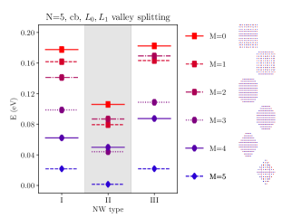
In Fig. 2 we show the valley splitting energies of the ground conduction multiplet as a function of the shape parameter in NWs of the first three types (see Table 1) with the shape parameter (approximate lateral size Å). The valley splittings are maximal in rectangular NWs () and almost absent in rhombic NWs (). These NWs have their surfaces terminated either by and facets, or mostly by facets, respectively. The very similar dependence on the parameter holds for each . Even thought the facets of PbSe are polar, in this work we assume that this charge is compensated and therefore neglect the built-in electric field. Note that the NWs of type III have one extra and one extra atomic planes compared to the NWs of type II, but their splitting energies of the ground multiplet are almost twice as large. The type IV is not shown here, as in this case the valley multiplet acquires an extra degeneracy due to the time reversal symmetry, see Appendix B.
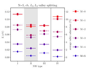
The valley splitting energies of the ground conduction multiplet as a function of the shape parameter in NWs with are summarized in Fig. 3. They are only about two thirds of the corresponding splittings of the multiplet, which is mostly due to the mass anisotropy. Indeed, the and valleys lie within (110) plane, while the and are tilted towards the wire axis and therefore have lighter effective in-plane masses, see (5). Also note, that there is almost no difference in splitting energies in the NWs of type II and III.
Now let us turn to the NWs of type IV, shown in right column in Fig. 3. In these NWs the and ground valley multiplet is split via completely different mechanism. Since inversion center in NWs of type IV is located between atoms (see Table. 1), the and valleys have different parity and can not mix directly. The parity of an valley is related to phase factors at lattice nodes. For , positions of the two closest to inversion center cations, these phases are for the valley and for the . This implies that valley is odd (even) and that the valley coupling in this case is only possible via far energy states.
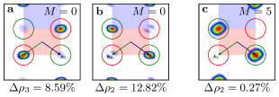
In fact, this possibility is realized and is the most pronounced in rectangular NWs (shape parameter ), similarly to the valley splittings. To illustrate this, in Fig. 4 we show the local density of states in reciprocal space (kLDOS, see Refs. Nestoklon et al. (2016); Avdeev et al. (2017) for details). For quantitative description of the valley coupling we introduce “valley admixture”
| (3) |
where is the valley density, integrated over small region near the valley shown by red (green) circles in Fig. 4. One can see that the valley admixture in rectangular NWs is much higher that in rhombic ones. The value in rhombic NW () is % and the corresponding kLDOS is not shown in Fig. 4. The density distributions near the main peaks in Figs. 4a–4c are -like (correspond to the ground multiplet), while distributions near the secondary peaks in Figs. 4a and 4b are - and -like, respectively. It proves that the admixed states belong to different valley multiplets. Note, for convenience in Fig. 3 we show the average valley admixtures for the NWs of type IV.
Before we discussed NWs with the size parameter (ten atomic layers along the and directions). Next, in Figs. 5 and 6 we show both size () and shape () dependencies of the valley splitting. We show the data only for the NWs of type II, since the others behave very similar. We vary the size parameter from to so the lateral size of NWs changes from Å2 to Å2 along the and axes respectively. In order to highlight the shape and size dependencies, in Figs. 5 and 6 we connect data points with the same parameter by color lines (solid red for , dashed blue for ). For each size parameter , the shape parameter satisfies , therefore each line in Figs. 5 and 6 starts from . The starting point of each line (except for and ) is indicated by marker.
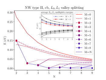
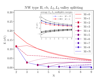
Fig. 5 shows the valley splitting energies of the ground conduction multiplet. Inset shows the average energies (without the valley splitting) of the two valley multiplets with lowest energies in conduction and valence bands in rectangular (, dashed lines) and rhombic (, solid lines) NWs as a function of size parameter . Average energies of the ground conduction multiplet are additionally indicated by color to match the main plot (red for , blue for ). Note, that the rhombic NWs exhibit larger confinement energies than their rectangular counterparts, while the valley mixing in rhombic NWs is strongly suppressed.
The same data for the ground conduction multiplet is shown in Fig. 6. We do not discuss it in details, but mention, that all the size and shape dependencies of the valley splitting (coupling) are almost the same, except for their absolute values. Therefore we conclude, that the shape induced suppression of the valley splitting in NWs is rather a physical phenomena.
IV Conclusion
We studied the valley splitting in -grown nanowires with different size, shape and symmetry. We demonstrate, that the valley splittings substantially depend on the NW shape, for particular case of prismatic octagonal NWs which is determined by relative fraction of facets compared to facets at the NW surface. The values of valley splittings are large, up to meV in NWs about nm diameter. The splittings tend to have maximal values in rectangular NWs ( and facets at the surface) and are almost absent in rhombic NWs (mostly facets at the surface). This result holds for a wide range of NW sizes and different point symmetries.
We also found a special type of NWs with non symmorphic spatial group, where valley multiplets become fourfold degenerate and the splitting of multiplets is due to the intervalley coupling via far energy states
Results of this work, except for the absolute values of the valley splittings, also apply for PbS and PbTe, due to the very similar band structures of these materials.
Acknowledgements.
The author acknowledges fruitful discussions with M. O. Nestoklon and financial support by RFBR Project No. 17-02-00383 A.Appendix A Microscopic wire structure
PbSe has the rocksalt crystal structure with
| (4) |
lattice vectors, where Å is the lattice constant Poddubny et al. (2012). Reciprocal lattice vectors are conveniently related with the valleys 1 as .
With the used tight binding parametrization Poddubny et al. (2012) the first conduction band effective mass ratios along the and directions ( NW axes) are
| (5) |
where denotes the effective mass along of the first conduction band electron at the valley.
The first three NW types, see Table 1, have , and point groups, respectively. Their symmetries are determined by orientation of axes and the position of the point symmetry origin relative to the cation, marked by “x” in Table 1. NW type I has inversion center, three rotation axes (in the NW coordinates frame) and three corresponding reflection planes . NW type II has rotation axis and reflection planes with the point symmetry origin being at . NW type III has rotation axis and reflection planes with the point symmetry origin being at .
NW type IV has non symmorphic spatial group with point symmetry. We use point (relative to the cation) as the point symmetry origin, which results in the following quotient group
| (6) |
Note, that this is not the only possible, but is the most convenient way to choose the point symmetry origin.
Appendix B Symmetry analysis
Symmetry analysis for the first three NW types is trivial and therefore omitted. Instead, we focus on the NW type IV to describe the absence of the valley splitting in valley multiplets.
Following ref. Bir and Pikus (1974), we use projective representations to classify the states of valley multiplets, because these valleys project onto the edge of the NW Brillouin zone. In there are two projective classes: and . Class has only one dimensional (vector and spinor) representations Koster et al. (1963), while in there is only one two-dimensional representation .
Since the valleys project onto the point, states of the multiplets belong to the class and can be classified according to ref. Koster et al. (1963). States of the valley multiplets belong to the class , and therefore transform according to . Indeed, the factor system
| (7) |
on elements (6) with or , (1), has the form
| (8) |
which is the standard form for the class Bir and Pikus (1974). Note, since all , the factor system depends only on projection of the wave vector onto the NW axis.
Next we consider time reversal symmetry by means of Herring criterion Herring (1937); Bir and Pikus (1974), which is about relation of and , where is the time reversal operator. The criterion reads as a sum over quotient group
| (9) |
There are three options: and are (a) llinearly dependent, (b) linearly independent and tranform according to conjugate representations or (c) equivalent representations. In cases (b) and (c) time reversal symmetry leads to additional degeneracy of states.
The fact that the factor system for multiplets, eq. (8), has the standard form, allow us to use the explicit form of generator matrices for representation from ref. Bir and Pikus (1974). With generators matrices the sum (9) for states is easily evaluated
| (10) |
and we see that the case (c) is realized. Here due to the antiunitary nature of time reversal operator for spinors. Therefore the states of multiplets are fourfold degenerate.
References
- Talapin and Murray (2005) Dmitri V. Talapin and Christopher B. Murray, “Pbse nanocrystal solids for n- and p-channel thin film field-effect transistors,” Science 310, 86–89 (2005).
- Kim et al. (2011) David K. Kim, Tarun R. Vemulkar, Soong Ju Oh, Weon-Kyu Koh, Christopher B. Murray, and Cherie R. Kagan, “Ambipolar and unipolar pbse nanowire field-effect transistors,” ACS Nano, ACS Nano 5, 3230–3236 (2011).
- Sukhovatkin et al. (2009) Vlad Sukhovatkin, Sean Hinds, Lukasz Brzozowski, and Edward H. Sargent, “Colloidal quantum-dot photodetectors exploiting multiexciton generation,” Science 324, 1542–1544 (2009).
- Padilha et al. (2010) Lazaro A. Padilha, Gero Nootz, Scott Webster, David J. Hagan, Eric W. Van Stryland, Larissa Levina, Vlad Sukhovatkin, and Edward H. Sargent, “Two-photon absorption and multi-exciton generation in lead salt quantum dots,” in Ultrafast Phenomena in Semiconductors and Nanostructure Materials XIV, edited by Jin-Joo Song, Kong-Thon Tsen, Markus Betz, and Abdulhakem Y. Elezzabi (SPIE-Intl Soc Optical Eng, 2010).
- Gesuele et al. (2012) Felice Gesuele, Chee Wei Wong, Matt Sfeir, Weon kyu Koh, Chris B. Murray, and Tony Heinz, “Ultrafast supercontinuum spectroscopy of multiple exciton states in lead chalcogenide nanorods and nanocrystals,” in Conference on Lasers and Electro-Optics 2012 (Optical Society of America, 2012) p. QM2G.2.
- Davis et al. (2015) Nathaniel J. L. K. Davis, Marcus L. Böhm, Maxim Tabachnyk, Florencia Wisnivesky-Rocca-Rivarola, Tom C. Jellicoe, Caterina Ducati, Bruno Ehrler, and Neil C. Greenham, “Multiple-exciton generation in lead selenide nanorod solar cells with external quantum efficiencies exceeding 120%,” Nature Communications 6, 8259 (2015).
- Lifshitz et al. (2003) E. Lifshitz, M. Bashouti, V. Kloper, A. Kigel, M. S. Eisen, and S. Berger, “Synthesis and characterization of PbSe quantum wires, multipods, quantum rods, and cubes,” Nano Letters 3, 857–862 (2003).
- Cho et al. (2005) Kyung-Sang Cho, Dmitri V. Talapin, Wolfgang Gaschler, and Christopher B. Murray, “Designing pbse nanowires and nanorings through oriented attachment of nanoparticles,” Journal of the American Chemical Society, Journal of the American Chemical Society 127, 7140–7147 (2005).
- Fardy et al. (2007) M. Fardy, A. I. Hochbaum, J. Goldberger, M. M. Zhang, and P. Yang, “Synthesis and thermoelectrical characterization of lead chalcogenide nanowires,” Advanced Materials 19, 3047–3051 (2007).
- Talapin et al. (2007) Dmitri V. Talapin, Heng Yu, Elena V. Shevchenko, Arun Lobo, and Christopher B. Murray, “Synthesis of colloidal pbse/pbs core−shell nanowires and pbs/au nanowire−nanocrystal heterostructures,” The Journal of Physical Chemistry C, The Journal of Physical Chemistry C 111, 14049–14054 (2007).
- Koh et al. (2010) Weon-kyu Koh, Adam C. Bartnik, Frank W. Wise, and Christopher B. Murray, “Synthesis of monodisperse PbSe nanorods: A case for oriented attachment,” J. Am. Chem. Soc. 132, 3909–3913 (2010).
- Akhtar et al. (2012) Javeed Akhtar, Masood Akhtar, Mohammad Azad Malik, Paul O’Brien, and James Raftery, “A single-source precursor route to unusual pbse nanostructures by a solution–liquid–solid method,” Journal of the American Chemical Society, Journal of the American Chemical Society 134, 2485–2487 (2012).
- Graham and Yu (2012) Rion Graham and Dong Yu, “High carrier mobility in single ultrathin colloidal lead selenide nanowire field effect transistors,” Nano Letters, Nano Letters 12, 4360–4365 (2012).
- Jun et al. (2006) Young-wook Jun, Jin-sil Choi, and Jinwoo Cheon, “Shape control of semiconductor and metal oxide nanocrystals through nonhydrolytic colloidal routes,” Angewandte Chemie International Edition 45, 3414–3439 (2006).
- Mokari et al. (2007) Taleb Mokari, Minjuan Zhang, and Peidong Yang, “Shape, size, and assembly control of pbte nanocrystals,” Journal of the American Chemical Society, Journal of the American Chemical Society 129, 9864–9865 (2007).
- Jawaid et al. (2011) Ali M. Jawaid, Daniel J. Asunskis, and Preston T. Snee, “Shape-controlled colloidal synthesis of rock-salt lead selenide nanocrystals,” ACS Nano 5, 6465–6471 (2011).
- Placencia et al. (2015) Diogenes Placencia, Janice E. Boercker, Edward E. Foos, and Joseph G. Tischler, “Synthesis and optical properties of PbSe nanorods with controlled diameter and length,” J. Phys. Chem. Lett. 6, 3360–3364 (2015).
- Jang et al. (2010) So Young Jang, Yun Mi Song, Han Sung Kim, Yong Jae Cho, Young Suk Seo, Gyeong Bok Jung, Chi-Woo Lee, Jeunghee Park, Minkyung Jung, Jinhee Kim, Bongsoo Kim, Jin-Gyu Kim, and Youn-Joong Kim, “Three synthetic routes to single-crystalline pbs nanowires with controlled growth direction and their electrical transport properties,” ACS Nano, ACS Nano 4, 2391–2401 (2010).
- An et al. (2007) J. M. An, A. Franceschetti, and A. Zunger, “The excitonic exchange splitting and radiative lifetime in pbse quantum dots,” Nano Letters 7, 2129–2135 (2007).
- Wei and Zunger (1997) Su-Huai Wei and Alex Zunger, “Electronic and structural anomalies in lead chalcogenides,” Phys. Rev. B 55, 13605–13610 (1997).
- Bartnik et al. (2010) A. C. Bartnik, Al. L. Efros, W.-K. Koh, C. B. Murray, and F. W. Wise, “Electronic states and optical properties of PbSe nanorods and nanowires,” Phys. Rev. B 82, 195313 (2010).
- Allan and Delerue (2004) G. Allan and C. Delerue, “Confinement effects in PbSe quantum wells and nanocrystals,” Phys. Rev. B 70, 245321 (2004).
- Nestoklon et al. (2006) M. O. Nestoklon, L. E. Golub, and E. L. Ivchenko, “Spin and valley-orbit splittings in SiGe/Si heterostructures,” Phys. Rev. B 73, 235334 (2006).
- An et al. (2006) J. M. An, A. Franceschetti, S. V. Dudiy, and Alex Zunger, “The peculiar electronic structure of pbse quantum dots,” Nano Letters, Nano Letters 6, 2728–2735 (2006).
- Paul and Klimeck (2011) Abhijeet Paul and Gerhard Klimeck, “Atomistic study of electronic structure of PbSe nanowires,” Applied Physics Letters 98, 212105 (2011).
- Poddubny et al. (2012) A. N. Poddubny, M. O. Nestoklon, and S. V. Goupalov, “Anomalous suppression of valley splittings in lead salt nanocrystals without inversion center,” Phys. Rev. B 86, 035324 (2012).
- Avdeev et al. (2017) I. D. Avdeev, A. N. Poddubny, S. V. Goupalov, and M. O. Nestoklon, “Valley and spin splittings in pbse nanowires,” Phys. Rev. B 96, 085310 (2017).
- Argeri et al. (2011) Mario Argeri, Alberto Fraccarollo, Fabio Grassi, Leonardo Marchese, and Maurizio Cossi, “Density functional theory modeling of pbse nanoclusters: Effect of surface passivation on shape and composition,” The Journal of Physical Chemistry C, The Journal of Physical Chemistry C 115, 11382–11389 (2011).
- Deringer and Dronskowski (2016) Volker L. Deringer and Richard Dronskowski, “Stabilities and reconstructions of clean pbs and pbse surfaces: Dft results and the role of dispersion forces,” The Journal of Physical Chemistry C 120, 8813–8820 (2016).
- Jancu et al. (1998) Jean-Marc Jancu, Reinhard Scholz, Fabio Beltram, and Franco Bassani, “Empirical tight-binding calculation for cubic semiconductors: General method and material parameters,” Phys. Rev. B 57, 6493–6507 (1998).
- Poddubny et al. (2017) Alexander N. Poddubny, Valentina M. Litvyak, Mikhail O. Nestoklon, Roman V. Cherbunin, Valerii V. Golubkov, Petr A. Onushchenko, Anastasiya N. Babkina, Alexei A. Onushchenko, and Serguei V. Goupalov, “Role of valley anisotropy in optical absorption of monodisperse pbs nanocrystals,” The Journal of Physical Chemistry C, The Journal of Physical Chemistry C 121, 27766–27773 (2017).
- Wrasse et al. (2011) E. O. Wrasse, R. J. Baierle, T. M. Schmidt, and A. Fazzio, “Quantum confinement and spin-orbit interactions in pbse and pbte nanowires: First-principles calculation,” Phys. Rev. B 84, 245324 (2011).
- Liu et al. (2018) Yun Liu, Donghun Kim, Owen P. Morris, David Zhitomirsky, and Jeffrey C. Grossman, “Origins of the stokes shift in pbs quantum dots: Impact of polydispersity, ligands, and defects,” ACS Nano, ACS Nano 12, 2838–2845 (2018).
- Hummer et al. (2007) Kerstin Hummer, Andreas Grüneis, and Georg Kresse, “Structural and electronic properties of lead chalcogenides from first principles,” Phys. Rev. B 75, 195211 (2007).
- Svane et al. (2010) A. Svane, N. E. Christensen, M. Cardona, A. N. Chantis, M. van Schilfgaarde, and T. Kotani, “Quasiparticle self-consistent GW calculations for PbS, PbSe, and PbTe: Band structure and pressure coefficients,” Phys. Rev. B 81, 245120 (2010).
- Zherebetskyy et al. (2014) Danylo Zherebetskyy, Marcus Scheele, Yingjie Zhang, Noah Bronstein, Christopher Thompson, David Britt, Miquel Salmeron, Paul Alivisatos, and Lin-Wang Wang, “Hydroxylation of the surface of pbs nanocrystals passivated with oleic acid,” Science (2014), 10.1126/science.1252727.
- Goupalov (2011) S. V. Goupalov, “Comment on “electronic structure and optical properties of quantum-confined lead salt nanowires”,” Phys. Rev. B 84, 037303 (2011).
- Avdeev and Nestoklon (2016) I D Avdeev and M O Nestoklon, “Electronic structure of PbSe nanowires,” Journal of Physics: Conference Series 769, 012074 (2016).
- Pawłowski et al. (2018) J. Pawłowski, D. Żebrowski, and S. Bednarek, “Valley qubit in a gated monolayer quantum dot,” Phys. Rev. B 97, 155412 (2018).
- YU and Cardona (2010) Peter YU and Manuel Cardona, Fundamentals of Semiconductors: Physics and Materials Properties, 4th ed. (Springer-Verlag Berlin Heidelberg, 2010).
- Koster et al. (1963) George F. Koster, John O. Dimmock, Robert G. Wheeler, and Hermann Statz, The Properties of the Thirty-Two Point Groups (M.I.T. Press, Cambridge, 1963).
- Nestoklon et al. (2016) M. O. Nestoklon, A. N. Poddubny, P. Voisin, and K. Dohnalova, “Tuning optical properties of ge nanocrystals by si shell,” The Journal of Physical Chemistry C 120, 18901–18908 (2016).
- Bir and Pikus (1974) G.L. Bir and G.E. Pikus, Symmetry and Strain-Induced Effects in Semiconductors (Wiley, New York, 1974).
- Herring (1937) Conyers Herring, “Effect of time-reversal symmetry on energy bands of crystals,” Phys. Rev. 52, 361–365 (1937).