Scanning Tunneling Thermometry
Abstract
Temperature imaging of nanoscale systems is a fundamental problem which has myriad potential technological applications. For example, nanoscopic cold spots can be used for spot cooling electronic components while hot spots could be used for precise activation of chemical or biological reactions. More fundamentally, imaging the temperature fields in quantum coherent conductors can provide a wealth of information on heat flow and dissipation at the smallest scales. However, despite significant technological advances, the spatial resolution of temperature imaging remains in the few nanometers range. Here we propose a method to map electronic temperature variations in operating nanoscale conductors by relying solely upon electrical tunneling current measurements. The scanning tunneling thermometer, owing to its operation in the tunneling regime, would be capable of mapping sub-angstrom temperature variations, thereby enhancing the resolution of scanning thermometry by some two orders of magnitude.
Thermal imaging of nanoscale systems is of crucial importance not only due to its potential to enable future technologies, but also because it can greatly enhance our understanding of heat transport at the smallest scales. In recent years, nanoscale thermometry has been used in a wide range of fields [1] including thermometry in a living cell [2], local control of chemical reactions [3] and temperature mapping of operating electronic devices [4]. Various studies utilize radiation-based techniques such as Raman spectroscopy [5], fluorescence in nanodiamonds [2, 6] and near-field optical microscopy [7]. The spatial resolution of these radiation-based techniques is limited due to optical diffraction and, to overcome this drawback, scanning probe techniques have seen a flurry of activity in recent years [8]. However, despite their remarkable progress, the spatial resolution remains in the range. A key obstacle to achieving high spatial resolution in scanning probe thermometry has been the fundamental difficulty in designing a thermal probe that exchanges heat with the system of interest but is thermally isolated from the environment.
Since temperature and voltage are both fundamental thermodynamic observables, it is instructive to draw the sharp contrast that exists between the measurement of these two quantities at the nanoscale. Scanning tunneling potentiometry (STP) [9] is a mature technology and can map local voltage variations with sub-angstrom spatial resolution by operating in the tunneling regime. STP has been used to map the local voltage variations in the vicinity of individual scatterers, interfaces or boundaries [10, 11, 12, 13, 14], providing direct observations of the Landauer dipole [15, 16]. STP has been a useful tool in disentangling different scattering mechanisms [14] and can map local potential variations due to quantum interference effects [12, 13]. Similarly, local temperature variations due to quantum interference effects have been theoretically predicted for various nanosystems out of equilibrium [17, 18, 19, 20] but have hitherto remained outside the reach of experiment.
Scanning thermal microscopy [21] (SThM) relies on the measurement of a heat-flux signal that can be sensed, e.g., by a calibrated thermocouple or an electrical resistor [22]. A good thermal contact between the tip and sample is needed for an appreciable heat flux and generally implies a measurement in the contact regime, thus limiting the spatial resolution. Despite the recent progress in adressing contact-related issues in SThM [8, 23], the best spatial resolution is presently [24].
It is well known that, outside equilibrium, the temperatures of different degrees of freemdom (e.g. phonon, photon, electron) do not coincide [25]; Existing SThM schemes cannot distinguish between the contributions of the different degrees of freedom to the heat-flux. A number of nanoscopic devices operate in the elastic transport regime where the electron and phonon degrees of freedom are completely decoupled and, consequently, the distinction between their temperatures becomes extremely important [26].
From a fundamental point of view, a thermometer is a device that equilibrates locally with the system of interest and has some temperature-dependent physical property (e.g. resistance, thermopower, mass density) which can be measured; the temperature measurement seeks to find the condition(s) under which the thermometer is in local thermodynamic equilibrium with the system of interest and concurrently infers the thermometer’s temperature by relying upon those temperature-dependent physical properties. Ideally, the measurement apparatus must not substantially disturb the state of the system of interest [27]. SThM schemes, by relying on heat fluxes in the contact regime, may alter the state of a small system. We propose here a noninvasive thermometer whose local equilibration can be inferred by the measurement of electrical tunneling currents alone. In particular, we find that the conditions required for the local equilibration of the scanning tunneling thermometer (STT) are completely determined by (a) the conductance and thermopower which are both measured using the tunneling current and (b) the bias conditions of the conductor defined by the voltages and temperatures of the contacts.
Our proposed method relies solely upon electrical measurements made in the tunneling regime and provides a measurement of the electronic temperature decoupled from all other degrees of freedom. We predict a dramatic enhancement of the spatial resolution by more than two orders of magnitude, thereby bringing thermometry to the sub-angstrom regime. The method is valid for systems obeying the Wiedemann-Franz (WF) law [28] which relates the electrical () and thermal conducatances () in a material-independent way . The WF law was first observed in bulk metals over 150 years ago and has been verified in a large number of nanoscale conductors. Most recently, it has been validated in atomic contact junctions [29, 30] which represent the ultimate limit of miniturization of electronic conductors.
Temperature measurement
We note a crucial, but often overlooked, theoretical point pertaining to the imaging of temperature fields on a nonequilibrium conductor. The prevailing paradigm for temperature and voltage measurements is the following [31]: (i) a voltage is measured by a probe (voltmeter) when in electrical equilibrium with the sample and (ii) a temperature is measured by a probe (thermometer) when in thermal equilibrium with the sample. We refer to this definition as the Engquist-Anderson (EA) definition.
The fact that the EA definition implicitly ignores thermoelectric effects was pointed out by Bergfield and Stafford [18, 32], and a notion of a joint probe was put forth by requiring both electrical and thermal equilibrium with the sample. It is quite easy to understand this intuitively: A temperature probe lacking local electrical equilibration with the sample develops a temperature bias at the probe-sample junction due to the Peltier effect; similarly, a voltage probe lacking local thermal equilibration with the sample develops a voltage bias at the probe-sample junction due to the Seebeck effect. These errors [32] can be quite large for systems with large thermoelectric responses. A temperature probe therefore has to remain in thermal and electrical equilibrium with the nonequilibrium sample [18, 19, 26, 27, 32, 33], thereby ensuring true thermodynamic equilibrium of the measurement apparatus.
The joint probe measurement was made mathematically rigorous in a recent study by Shastry and Stafford [27] where it was shown that the solution to the probe equilibration problem always exists and is unique, arbitrarily far from equilibrium and with arbitrary interactions within the quantum system. Moreover, it was shown that the EA definition is provably nonunique: The value measured by the EA thermometer depends quite strongly on its voltage and, conversely, the value measured by the EA voltmeter depends on its temperature. These results are intimately connected to the second law of thermodynamics and expose the fatal flaw in the EA definition: the measurement apparatus (thermometer or voltmeter) has to remain in thermodynamic equilibrium, i.e., electrical and thermal equilibrium, with the system of interest which it probes locally. Simply stated, an open system of electrons (a conductor) exchanges both charge and heat. We therefore write
| (1) |
for the simultaneous vanishing of the electric current and the electronic contribution to the heat current flowing into the probe . The above equation determines the conditions under which a local thermodynamic equilibrium is established between the probe (STT) and the nonequilibrium system of interest.
Temperature from tunneling currents
The probe currents depend linearly on the temperature and voltage gradients for transport within the linear response regime:
| (2) |
where the are the Onsager linear response coefficients evaluated at the equilibrium temperature and chemical potential . is the electrical conductance () between the probe and contact . is related to the thermopower () and electrical conductance (). Finally, is related to the thermal conductance () up to leading order in the Sommerfeld series [28] (see also the Supplementary Information).
We solve for the temperature of the STT in Eq. (1) and find [19]
| (3) | ||||
Here denotes the exact solution to the equilibration of the STT, i.e., Eq. (1), within the linear response regime where the currents are expressed by Eq. (2).
Eq. (2) suggests that and can be measured using the tunneling current , whereas appears only in the expression for the heat current and would generally involve the measurement of a heat-flux-related signal. However, for systems obeying the WF law, we may simply relate and using
| (4) |
valid up to leading order in the Sommerfeld series. This allows us to infer using the WF law given by Eq. (4) and we obtain
| (5) | ||||
valid up to leading order in the Sommerfeld series.
requires only the measurement of and , or equivalently, the electrical conductance and thermopower, and lends itself to a simple interpretation: The first term in Eq. (5) is the thermoelectric contribution whereas the second term is the thermal contribution. The second-order corrections in the Sommerfeld series are typically very small
| (6) |
where the characteristic energy scale of the problem is typically much larger than the thermal energy set by : e.g., , the Fermi energy, for bulk systems and for a tunneling probe is of the order of the work function. The breakdown of the Wiedemann-Franz law has been reported in various nanoscale systems. The characteristic energy scale in such cases is comparable to the thermal energy thereby leading to large errors in the Sommerfeld series expansion in Eq. (6). In graphene, the breakdown of the WF law was reported in Ref. [34]. Here, the local chemical potential was tuned (via local doping) such that it is smaller than the thermal energy thereby creating the so-called Dirac fluid. Such systems show a decoupling of charge and heat currents, making it impossible to measure heat currents through electrical means. Although our results apply to a broad array of nanoscale conductors, they do not apply to systems prepared in this manner.
It is clear from Eq. (5) that the measurement of (a) conductance and the thermoelectric coefficient along with the (b) known bias conditions of the system completely determine the conditions under which the STT is in local thermodynamic equilibrium with the system.
Experimental Implementation
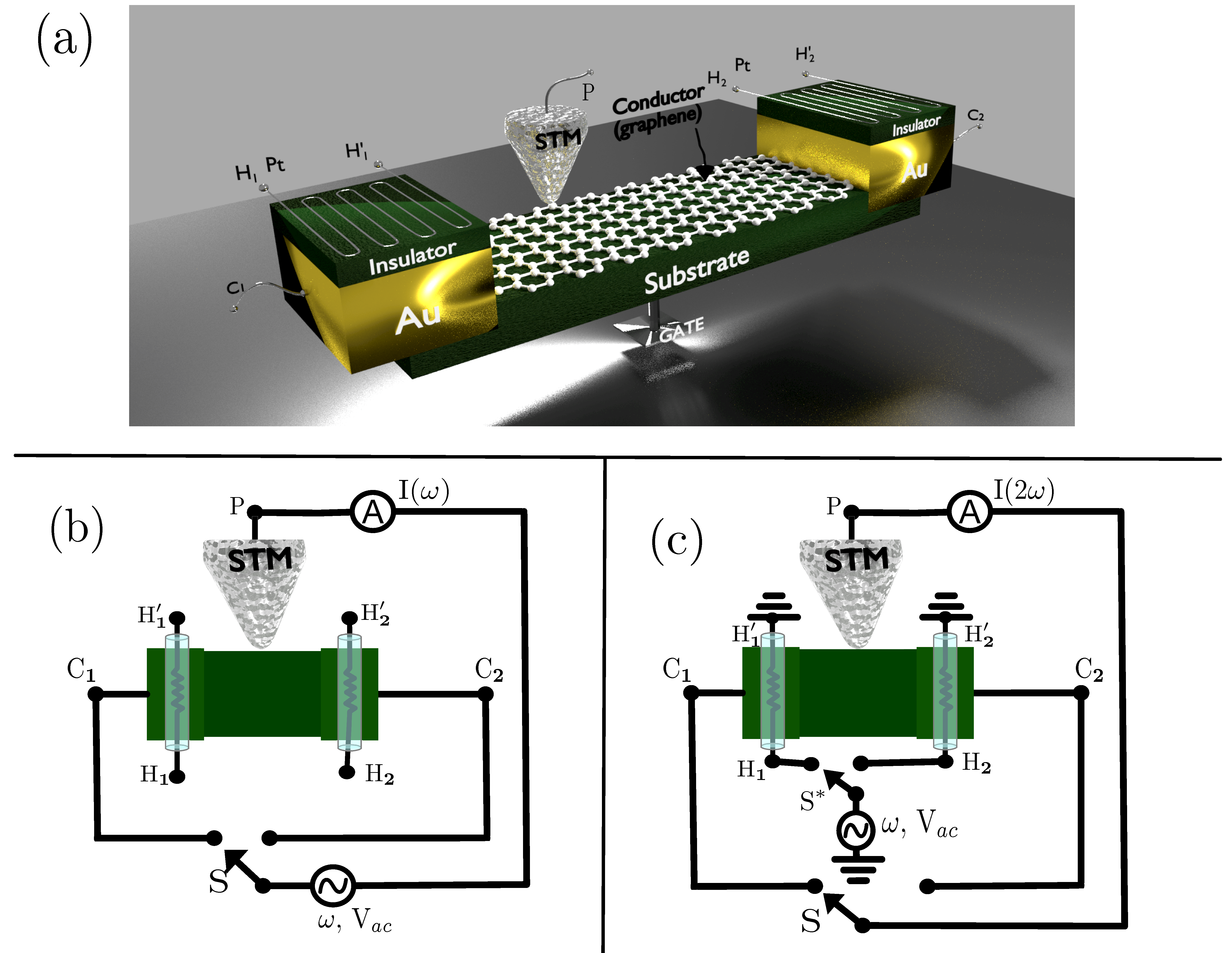
The temperature measurement involves two circuits: (I) The conductance circuit which measures the electrical conductance and (II) The thermoelectric circuit which measures the thermoelectric response coefficient , as shown in Fig. 1 (b) and (c) respectively. The STT involves operating the tip of a scanning tunneling microscope (STM) at a constant height above the surface of the conductor in the tunneling regime. The circuit operations (I) and (II) are described below.
(I) The conductance circuit involves a closed circuit of the probe and the contact . All contacts and the probe are held at the equilibrium temperature . An ac voltage is applied at the probe-contact junction and the resulting tunneling current is recorded using standard lock-in techniques. The STM tip is scanned along the surface. A switch disconnects all contacts except and the tunneling current is therefore
| (7) | ||||
The procedure is repeated for all the contacts by toggling the switch S shown in Fig. (1b) and a scan is obtained for each probe-contact junction. This completes the measurement of the conductance for all the contacts .
(II) The thermoelectric circuit involves a (i) closed circuit of the probe and contact , which is the same as the conductance circuit without the voltage source, and (ii) an additional circuit which induces time-modulated temperature variations in contact ; An ac current at frequency induces Joule heating in the Pt resistor at frequency and results in a temperature modulation in the contact . The probe is held at the equilibrium temperature . The resulting tunneling current , at frequency , is recorded using standard lock-in techniques. The STM tip is scanned along the surface at the same points as before. A switch disconnects all contacts except and the tunneling current is
| (8) | ||||
The procedure is repeated for all the contacts by toggling the switches S and S* shown in Fig. (1c) and a scan is obtained for each probe-contact junction. Note that the switch S* must heat the Pt resistor in the same contact for which the probe-contact tunneling current is measured. This completes the measurement of the thermoelectric coefficient for all the contacts .
Heating elements have been fabricated in the contacts previously [35]. Any system where one may induce Joule heating can be used as the heating element (instead of Pt) in the circuit. For example, another flake of graphene could be used as a heating element as long as it is calibrated accurately. The voltage modulation frequency in the heating elements , where is the thermal time constant of the contacts, so that the contact may thermalize with the heating element. Typically, is of the order of tens of nanoseconds (cf. methods in [18]). We discuss the calibration of the contact temperature in the Supplementary Information. The thermoelectric response of the nanosystem may be quite sensitive to the gate voltage which is also discussed in the Supplementary Information.
Results
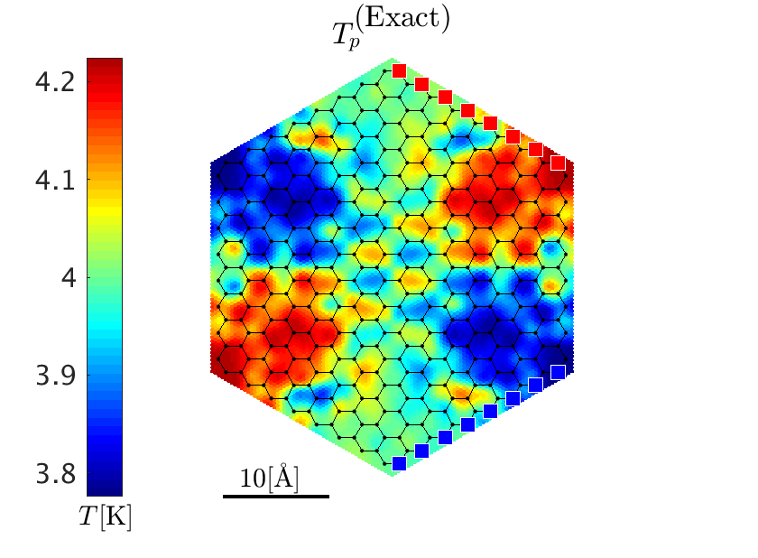
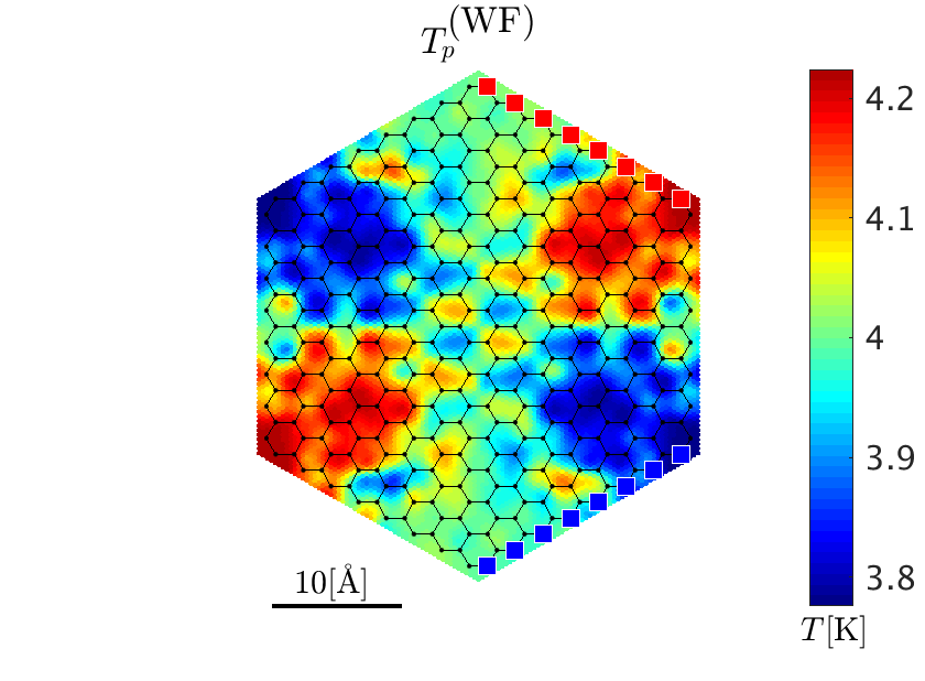
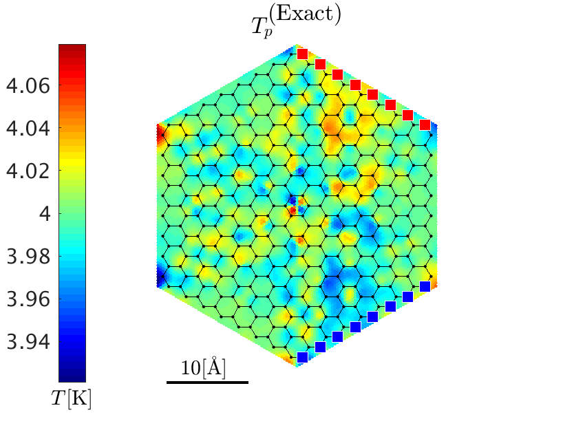
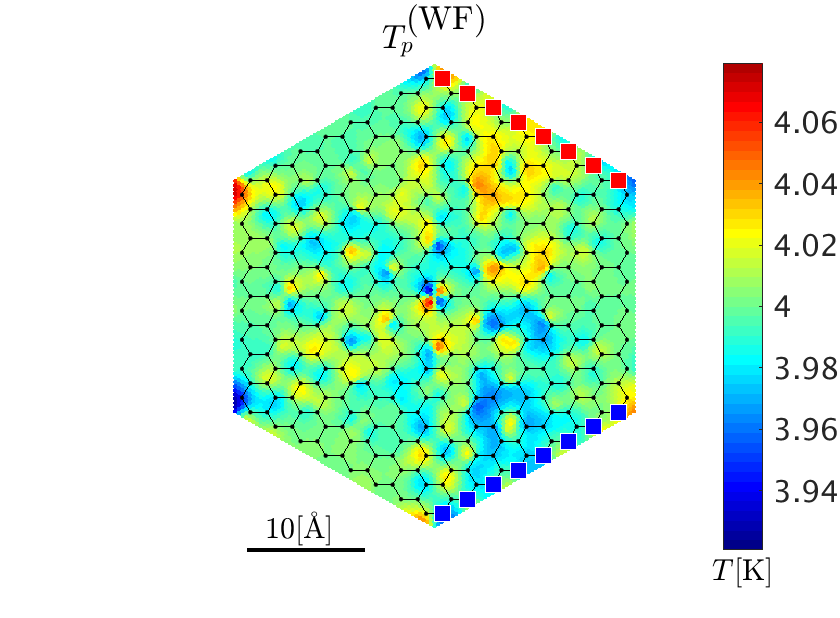
We present model temperature measurements for a hexagonal graphene flake under (a) a thermal bias and (b) a voltage bias. The measured temperature, for a combination of thermal and voltage biases, would simply be a linear combination of the two scenarios (a) and (b) in the linear response regime (under identical gating conditions). Therefore, we present the two cases separately but we note that the gate voltages are not the same for the two scenarios that we present here. The voltage bias case has been gated differently so as to enhance the thermoelectric response of the system. We show the temperature measurement for (a) the thermal bias case in Fig. 2 and (b) the voltage bias case in Fig. 3. The two panels in Figs. 2 and 3 compare (1) the temperature measurement obtained from the exact solution [given by Eq. (3)] and (2) the temperature measurement obtained from our method [given by Eq. (5)] which relies on the WF law.
Graphene is highly relevant for future electronic technologies and provides a versatile system whose transport properties can be tuned by an appropriate choice of the gate voltage — we therefore illustrate our results for graphene. The method itself is valid for any system obeying the WF law. The thermoelectric response coefficient has a quadratic suppression at low temperatures and its measurement from Eq. (8) depends crucially on the choice of gating especially at cryogenic operating temperatures since the resulting tunneling current must be experimentally resolvable. In graphene, we find that the electrical tunneling currents arising from its thermoelectric response are resolvable even at cryogenic temperatures when the system is gated appropriately and, owing to the fact that a number of STM experiments are conducted at low temperatures, we present our results for . Higher operating temperatures result in a higher tunneling current in Eq. (8) and gating would therefore be less important.
The -electron system of graphene is described using the tight-binding model whose basis states are orbitals at each atomic site of carbon. The STT is modeled as an atomically sharp Pt tip operating at a constant height of above the plane of the carbon nuclei. The details of the graphene Hamiltonian as well as the probe-system tunnel coupling are presented in the Methods section. The atomic sites of graphene which are coupled to the contacts are indicated in Figs. 2 and 3 by either a red or blue square. The chemical potential and temperature of the two contacts (red and blue) set the bias conditions for the problem. The coupling to the two contacts is symmetrical and the coupling strength for all the coupling sites (red or blue) is taken as . Additional details regarding the gating and the tunneling currents are included in the Supplementary Information.
Fig. 2 shows the variations in temperature for a symmetrical () temperature bias . The agreement between and given by Eqs. (3) and (5) respectively is excellent. The gating has been chosen to be with respect to the Dirac point in graphene. The same temperature scale is used for both the panels in Fig. 2. The temperature variations in are solely the result of the temperature bias and are given by the second term in Eq. (5). Therefore, we require only the measurement of the conductances for the temperature measurement under these bias conditions. We consider a contact-tip voltage modulation of for the measurement of the conductance. The resulting tunneling currents are of the order of with a maximum tunneling current of about . We present the details in the Supplemental Information.
Fig. 3 shows the variations in temperature for a voltage bias of , with , so that the transport is within the linear response regime. The gating for this case has been chosen to be such that there is an enhanced thermoelectric effect. The tunneling currents from the thermoelectric circuit, under these gating conditions, are of the order of with a maximum tunneling current of about and are resolvable under standard lock-in techniques. The variation of the contact temperature is taken to be with . The resolution of the tunneling current is an important point especially for the measurement of the thermoelectric response coefficient and has been covered in greater detail in the Supplementary Information. The same temperature scale is used for both panels in Fig. 3 and there is excellent agreement between and . The temperature variations shown here are solely the result of the voltage bias and are given by the first term in Eq. (5). Since the variations are purely due to the thermoelectric effect, the EA definition would have noted no temperature variations at all.
The disagreement between the exact solution and our method are due to higher-order contributions in the Sommerfeld series which are extremely small [cf. Eq. (6)]. An explicit expression for the first Sommerfeld correction in the WF law has been derived in the Supplementary Information. The discrepency between and defined by is less than for the temperature bias case in Fig. 2, whereas their discrepency for the voltage bias case in Fig. 3 is less than .
Conclusion
It has proven extraordinarily challenging to achieve high spatial resolution in thermal measurements. A key obstacle has been the fundamental difficulty in designing a thermal probe that exchanges heat with the system of interest but is thermally isolated from the environment. We propose circumventing this seemingly intractable problem by inferring thermal signals using purely electrical measurements. The basis of our approach is the Wiedemann-Franz law relating the thermal and electrical currents flowing between a probe and the system of interest.
We illustrate this new approach to nanoscale thermometry with simulations of a scanning tunneling probe of a model nanostructure consisting of a graphene flake under thermoelectric bias. We show that the local temperature inferred from a sequence of purely electrical measurements agrees exceptionally well with that of a hypothetical thermometer coupled locally to the system and isolated from the environment. Moreover, our measurement provides the electronic temperature decoupled from all other degrees of freedom and can therefore be a vital tool to characterize nonequilibrium device performance. Our proposed scanning tunneling thermometer exceeds the spatial resolution of current state-of-the-art thermometry by some two orders of magnitude.
Methods
System Hamiltonian
The -electron system of graphene is described within the tight-binding model, , with nearest-neighbor hopping matrix element eV. The coupling of the system with the contact reservoirs is described by the tunneling-width matrices . We calculate the transport properties using nonequilibrium Green’s functions. The retarded Green’s function of the junction is given by , where is the tunneling self-energy. We take the contact-system couplings in the broad-band limit, i.e., where is the Fermi energy of the metal leads. We also take the contact-system couplings to be diagonal matrices coupled to -orbitals of the graphene system. The nonzero elements of () are at sites indicated by either a blue or red square in figs. 2 and 3, corresponding to the carbon atoms of graphene covalently bonded to the contact reservoirs. The tunneling matrix element at each coupling site is set as for both the contacts (blue and red). is the overlap-matrix between the atomic orbitals on different sites and we take , i.e., an orthonormal set of atomic orbitals. The tunneling-width matrix describing the probe-sample coupling is also treated in the broad-band limit. The probe is in the tunneling regime and the probe-system coupling is weak (few meV) in comparison to the system-reservoir couplings.
Probe-Sample Coupling
The scanning tunneling thermometer is modeled as an atomically sharp Pt tip operating in the tunneling regime at a height of above the plane of the carbon nuclei in graphene. The probe tunneling-width matrices may be described in general as [36] , where is the local density of states of the apex atom in the probe electrode and , are the tunneling matrix elements between the l-orbital of the apex atom in the probe and the , -orbitals in graphene. The constants and has been determined by matching with the peak of the experimental conductance histogram [37]. We consider the Pt tip to be dominated by the d-orbital character (80%) although other contributions (s – 10% and p – 10%) are also taken as described in Ref. [36]. In the calculation of the tunneling matrix elements, the -orbitals of graphene are taken to be hydrogenic orbitals with an effective nuclear charge [38]. The tunneling-width matrix describing the probe-system coupling is in general non-diagonal.
Acknowledgements
The authors gratefully acknowledge useful discussions with Brian J. LeRoy and Oliver L.A. Monti. This work was supported by the U.S. Department of Energy (DOE), Office of Science, under Award No. DE-SC0006699.
References
- [1] Carlos D. S. Brites, Patricia P. Lima, Nuno J. O. Silva, Angel Millan, Vitor S. Amaral, Fernando Palacio, and Luis D. Carlos. Thermometry at the nanoscale. Nanoscale, 4:4799–4829, 2012.
- [2] G. Kucsko, P. C. Maurer, N. Y. Yao, M. Kubo, H. J. Noh, P. K. Lo, H. Park, and M. D. Lukin. Nanometre-scale thermometry in a living cell. Nature, 500(7460):54–58, Aug 2013. Letter.
- [3] C. Yan Jin, Zhiyong Li, R. Stanley Williams, K.-Cheol Lee, and Inkyu Park. Localized temperature and chemical reaction control in nanoscale space by nanowire array. Nano Letters, 11(11):4818–4825, 2011. PMID: 21967343.
- [4] Matthew Mecklenburg, William A. Hubbard, E. R. White, Rohan Dhall, Stephen B. Cronin, Shaul Aloni, and B. C. Regan. Nanoscale temperature mapping in operating microelectronic devices. Science, 347(6222):629–632, 2015.
- [5] J. S. Reparaz, E. Chavez-Angel, M. R. Wagner, B. Graczykowski, J. Gomis-Bresco, F. Alzina, and C. M. Sotomayor Torres. A novel contactless technique for thermal field mapping and thermal conductivity determination: Two-laser raman thermometry. Review of Scientific Instruments, 85(3):034901, 2014.
- [6] P. Neumann, I. Jakobi, F. Dolde, C. Burk, R. Reuter, G. Waldherr, J. Honert, T. Wolf, A. Brunner, J. H. Shim, D. Suter, H. Sumiya, J. Isoya, and J. Wrachtrup. High-precision nanoscale temperature sensing using single defects in diamond. Nano Letters, 13(6):2738–2742, 2013. PMID: 23721106.
- [7] D. Teyssieux, L. Thiery, and B. Cretin. Near-infrared thermography using a charge-coupled device camera: Application to microsystems. Review of Scientific Instruments, 78(3):034902, 2007.
- [8] Séverine Gomès, Ali Assy, and Pierre-Olivier Chapuis. Scanning thermal microscopy: A review. physica status solidi (a), 212(3):477–494, 2015.
- [9] P. Muralt and D. W. Pohl. Scanning tunneling potentiometry. Applied Physics Letters, 48(8):514–516, 1986.
- [10] B. G. Briner, R. M. Feenstra, T. P. Chin, and J. M. Woodall. Local transport properties of thin bismuth films studied by scanning tunneling potentiometry. Phys. Rev. B, 54:R5283–R5286, Aug 1996.
- [11] Geetha Ramaswamy and A. K. Raychaudhuri. Field and potential around local scatterers in thin metal films studied by scanning tunneling potentiometry. Applied Physics Letters, 75(13):1982–1984, 1999.
- [12] Weigang Wang, Ko Munakata, Michael Rozler, and Malcolm R. Beasley. Local Transport Measurements at Mesoscopic Length Scales Using Scanning Tunneling Potentiometry. Physical Review Letters, 110(23), jun 2013.
- [13] Kendal W. Clark, X.-G. Zhang, Gong Gu, Jewook Park, Guowei He, R. M. Feenstra, and An-Ping Li. Energy gap induced by friedel oscillations manifested as transport asymmetry at monolayer-bilayer graphene boundaries. Phys. Rev. X, 4:011021, Feb 2014.
- [14] Philip Willke, Thomas Druga, Rainer G. Ulbrich, M. Alexander Schneider, and Martin Wenderoth. Spatial extent of a landauer residual-resistivity dipole in graphene quantified by scanning tunnelling potentiometry. Nature Communications, 6:–, March 2015.
- [15] R. Landauer. Spatial variation of currents and fields due to localized scatterers in metallic conduction. IBM Journal of Research and Development, 1(3):223–231, July 1957.
- [16] M. Büttiker. Chemical potential oscillations near a barrier in the presence of transport. Phys. Rev. B, 40(5):3409–3412, Aug 1989.
- [17] Yonatan Dubi and Massimiliano Di Ventra. Thermoelectric effects in nanoscale junctions. Nano Letters, 9:97–101, 2009.
- [18] Justin P. Bergfield, Shauna M. Story, Robert C. Stafford, and Charles A. Stafford. Probing maxwell’s demon with a nanoscale thermometer. ACS Nano, 7(5):4429–4440, 2013.
- [19] J. Meair, J. P. Bergfield, C. A. Stafford, and Ph. Jacquod. Local temperature of out-of-equilibrium quantum electron systems. Phys. Rev. B, 90:035407, Jul 2014.
- [20] Justin P. Bergfield, Mark A. Ratner, Charles A. Stafford, and Massimiliano Di Ventra. Tunable quantum temperature oscillations in graphene nanostructures. Phys. Rev. B, 91:125407, Mar 2015.
- [21] C. C. Williams and H. K. Wickramasinghe. Scanning thermal profiler. Applied Physics Letters, 49(23):1587–1589, 1986.
- [22] A Majumdar. Scanning thermal microscopy. Annual Review of Materials Science, 29:505–585, 1999.
- [23] Fabian Menges, Heike Riel, Andreas Stemmer, and Bernd Gotsmann. Nanoscale thermometry by scanning thermal microscopy. Review of Scientific Instruments, 87(7):074902, 2016.
- [24] Fabian Menges, Philipp Mensch, Heinz Schmid, Heike Riel, Andreas Stemmer, and Bernd Gotsmann. Temperature mapping of operating nanoscale devices by scanning probe thermometry. Nature Communications, 7:10874 EP –, Mar 2016. Article.
- [25] J Casas-Vázquez and D Jou. Temperature in non-equilibrium states: a review of open problems and current proposals. Reports on Progress in Physics, 66(11):1937, 2003.
- [26] Charles A. Stafford. Local temperature of an interacting quantum system far from equilibrium. Phys. Rev. B, 93:245403, Jun 2016.
- [27] Abhay Shastry and Charles A. Stafford. Temperature and voltage measurement in quantum systems far from equilibrium. Phys. Rev. B, 94:155433, Oct 2016.
- [28] Neil W. Ashcroft and N. David Mermin. Solid State Physics. Brooks/Cole - Thomson Learning, 1976.
- [29] Nico Mosso, Ute Drechsler, Fabian Menges, Peter Nirmalraj, Siegfried Karg, Heike Riel, and Bernd Gotsmann. Heat transport through atomic contacts. Nat Nano, 12(5):430–433, May 2017. Letter.
- [30] Longji Cui, Wonho Jeong, Sunghoon Hur, Manuel Matt, Jan C. Klöckner, Fabian Pauly, Peter Nielaba, Juan Carlos Cuevas, Edgar Meyhofer, and Pramod Reddy. Quantized thermal transport in single-atom junctions. Science, 355(6330):1192–1195, 2017.
- [31] H.-L. Engquist and P. W. Anderson. Definition and measurement of the electrical and thermal resistances. Phys. Rev. B, 24:1151–1154, Jul 1981.
- [32] Justin P. Bergfield and Charles A. Stafford. Thermoelectric corrections to quantum voltage measurement. Phys. Rev. B, 90:235438, Dec 2014.
- [33] Abhay Shastry and Charles A. Stafford. Cold spots in quantum systems far from equilibrium: Local entropies and temperatures near absolute zero. Phys. Rev. B, 92:245417, Dec 2015.
- [34] Jesse Crossno, Jing K. Shi, Ke Wang, Xiaomeng Liu, Achim Harzheim, Andrew Lucas, Subir Sachdev, Philip Kim, Takashi Taniguchi, Kenji Watanabe, Thomas A. Ohki, and Kin Chung Fong. Observation of the dirac fluid and the breakdown of the wiedemann-franz law in graphene. Science, 351(6277):1058–1061, 2016.
- [35] Makusu Tsutsui, Tomoji Kawai, and Masateru Taniguchi. Unsymmetrical hot electron heating in quasi-ballistic nanocontacts. Scientific Reports, 2, Jan 2012.
- [36] Justin P. Bergfield, Joshua D. Barr, and Charles A. Stafford. Transmission eigenvalue distributions in highly conductive molecular junctions. Beilstein Journal of Nanotechnology, 3:40–51, 2012.
- [37] M. Kiguchi, O. Tal, S. Wohlthat, F. Pauly, M. Krieger, D. Djukic, J. C. Cuevas, and J. M. van Ruitenbeek. Highly conductive molecular junctions based on direct binding of benzene to platinum electrodes. Phys. Rev. Lett., 101:046801, 2008.
- [38] J. D. Barr, C. A. Stafford, and J. P. Bergfield. Effective field theory of interacting electrons. Phys. Rev. B, 86:115403, Sep 2012.