Robust -orbital half-metallicity and high Curie-temperature in the hole-doped anisotropic () nanosheets
Abstract
Here, we study the magnetism of the distorted 1- (=S,Se) based on first-principles calculation. The magnetism originates from the hole doping due to the density of states near the valence band edge having van Hove singularity feature. The calculated results show that the monolayer can develop an interesting ferromagnetic (FM) half-metallic phase with tunable spin-polarization orientation. The FM half-metallicity and magnetic moments of the hole-doped monolayer are primarily derived from the orbital of S atoms, then, a FM ground phase with a high Curie temperature () (larger than 800 K) is obtained due to the strong - direct exchange interaction. The magnetic order is robust against thermal excitations at finite temperatures because of magnetic anisotropic energy. In the bilayer, the electrons near Fermi level are redistributed when introducing the interlayer interaction, which suppresses the ferromagnetism induced by hole doping. The ferromagnetism can be recovered when the interlayer interaction is weakened.
keywords:
van Hove singularity, hole doping , half-metallicity , orbital, magnetic anisotropic energy , interlayer interaction1 INTRODUCTION
Spintronics, which takes advantage of the spin degree of freedom of electrons for delivering and storing information, have attracted great interest in science and technology. It requires the precise control of magnetic properties in low dimensions with high Curie temperature () for fabricating spintronic devices at the nanoscale. Half metals (HMs) are a kind of important spintronic materials with one spin channel being metallic and opposite spin channel being semiconducting. They can provide the single-spin transport that is demanded in future nanoelectric devices, such as spin-polarized tips in scanning tunneling microscopy. For the practical spintronics application at the nanoscale, the two dimensional (2D) materials should possess the following important feature:(i) a stable ferromagnetic (FM) half-metallic ground phase; (ii) a beyond room temperature. In decades, tremendous new 2D materials have been predicated theoretically and realized experimentally[1, 2, 3, 4, 5, 6, 7, 8, 9]. These materials hold tremendous potential applications in the next-generation high-performance electronics and optoelectronics[10, 11, 12, 13]. However, most of them are limited for practical applications in spintronics due to the absence of ferromagnetism. The experimental discovery of exfoliated 2D intrinsic FM materials [14] and [15] has inspired researchers to hunt for more realizable 2D magnetic materials. Although the high intrinsic ferromagnetism in 2D ScCl monolayer is predicated theoretically[16] and the ferromagnetic ordering of monolayer is maintained above room temperature[17], the magnetism originates from orbital which is not advantageous to low energy cost. Compared to the -orbital counterpart, the orbital magnetic materials can have a higher Fermi velocity and longer spin coherence length due to greater delocalization of orbital, which are advantageous for high-speed and long distance spin-polarized transport. In fact, 2D -orbital magnetism is available in graphene, silicene, phosphorene, etc. by many methods, such as introducing defects[18, 19, 20], adatoms[21, 22, 23, 24], or edges[25]. However, these modified materials are hard to synthesize experimentally due to the uncontrollability of modification. Very recently, a new class of 2D materials are found to possess novel band structure with a flat band edge. This leads to high density of states (DOS) and a sharp van Hove singularity at or near the Fermi level. The high DOS system would lead to an electronic instability, which leads to superconductivity, magnetism and other phenomena[26, 27, 28]. This offers a promising approach to develop controllable magnetism by carrier doping, where the carrier doping density can be controlled by gating technique. From first-principles calculations results, the GaSe[26], [29], [30], [31, 32], the -SnO[33], SiC[34] and monolayer[35] show ferromagnetism and half metallicity with carrier doping. Nevertheless, their half-metallic phases are unstable or the is rather low. Therefore, it remains challenging to obtain robust -orbital FM half-metallicity and high in 2D crystals for spintronic devices.
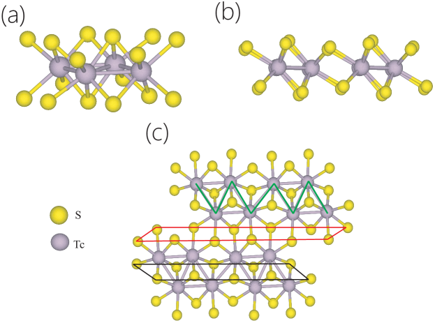
The family of transition metal dichalcogenides (TMDs) has been studied intensively because of the rich physics and tremendous potential for application, such as superconductivity[36] and charge density waves[37, 38]. Traditional TMDs adopt a sandwich-type structure where the metal atoms are located in between two layers of chalcogen atoms and exhibit isotropic behavior owing to high lattice symmetries, which determine their fundamental properties. Among the large family of TMDs, some compounds with low symmetry show more interesting anisotropic properties of both scientific and technologic importance. For example, the distorted lattice structure displays half metallicity and large magnetoresistance effect[39], the single-layer with low symmetry exhibit competitive performance with large current on/off ratios and low subthreshold swings, and a rich Raman spectrum with good signal strength[40]. Similar to bulk, the crystal structure of and bulks are triclinic with low symmetry (space group P), a stable phase with distorted 1T geometry, as shown in Fig. 1(a). In contrast to traditional TMDs, they possess larger and asymmetrical unit cells, corrugated surfaces, highly anisotropic structure, and metal-metal bonds. The and monolayer have been predicated with extracting from bulk form using the first principle calculations, the optical properties were also reported[41]. However, the magnetism of and monolayer have not been explored.
In this work, we systematically explore the magnetism of system with hole doping from first-principles calculations. In the monolayer, the system develops the FM HM over a significant range of hole doping density. More interestingly, the spin-polarization orientation of metallic band can be manipulated. Furthermore, the magnetism arises from the -orbital of S atoms, which realizes strong -orbital magnetism. The is far beyond room temperature. We also study the strain effect on magnetization, spin polarization energy, magnetic anisotropic energy (MAE), and . On the other hand, we find that the interlayer interaction suppresses FM phase in the bilayer. The magnetic state can be reproduced with weakening the interlayer interaction.
2 METHODS
Our first-principles calculations are based on the density functional theory (DFT) as implemented in the Vienna ab initio simulation package (VASP)[42, 43]. The ion-electron interactions is treated by projector augmented-wave (PAW) method[44]. The electron exchange correlation potential is treated with the generalized gradient approximation (GGA) of the Perdew-Bruke-Ernzerhof (PBE) functional[45]. Since the band structure is central to our study, we also perform Hybrid DFT calculations based on the Heyd-Scuseria-Ernzerhof (HSE06) exchange correlation functional[46]. A kinetic cutoff energy is set at 550 eV for the Kohn-Sham orbitals being expanded in the plane-wave basis. The lattice constants and the atomic positions are fully optimized with a conjugated gradient algorithm until the Hellman-Feynman forces are less than 0.01 eV/Å. The interlayer interaction is described with van der Waals (VDW) forces in the DFT-D2 approximation. The convergence criterion for self-consistent field (SCF) energy is set to eV. For Brillouin-zones integration, we employ a -centered Monkhorst-Pack algorithm -points grid and adopt the tetrahedron method with Blöchl corrections. To calculate the MAE, we include the spin-orbit coupling (SOC) in the calculations. The energy convergence criterion is promoted to eV, and the -points grid is enlarged to for calculating the MAE. In our calculation, the hole doping is simulated via changing the total number of electrons in the system, the charge neutrality is maintained by a compensating jellium background.
3 RESULTS AND DISCUSSION
3.1 Electronic structure
The optimized lattice parameters (, and ) for and bulks in our calculations are relatively smaller than those in previous DFT calculations[47]. This is because that the van der Waals forces are considered in our calculations, which could better describe the layer-layer interaction in materials compared with previous theoretical study with the standard DFT method. The band structures of and bulk obtained from PBE calculations indicate that they are both indirect semiconductors with a band gap of 1.04 and 0.86 eV, respectively. Moreover, they are slightly larger than that of previous DFT calculation (0.9 and 0.8 eV). However, the calculated structure parameters and band gap agree well with experimental values (1.0 and 0.88 eV)[48, 49] (see the Table S1 and Figure S1 in the Supplemental Material). These results show that the PBE calculation is sufficient to accurately describe the structures of and bulks. Given the good agreement between theory and experiment, we expect that the PBE is also suitable to investigate the electronic and magnetic property of the single-layer and . In the following, we take the monolayer as a prototype to discuss its band structure and magnetic properties.
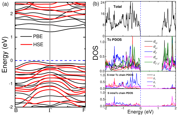
The crystal structure of monolayer is illustrated in Figs. 1(b) and 1(c). The unit cell consists of two hexagonal planes of eight S atoms and an intercalated hexagonal plane of four Tc atoms bound with S atoms forming diamond-shaped chains which are derived from the metal-metal bonds. The symmetry of the monolayer crystal is reduced from the 1T structure to the distorted 1T phase. The calculated two principal and axes are and Å, respectively. The calculated electronic band structure is displayed in Fig. 2(a), which shows that the valence band maximum (VBM) is situated at midpoint along the -B (0.5, 0.0, 0.0) symmetry line, while the conduction band minimum (CBM) is situated at the point. The monolayer has an indirect band gap of 1.28eV. These values are consistent with that of previous report[41]. More interestingly, one band has almost flat dispersion along the -F (0.0, 0.5, 0.0) symmetry line near the Fermi level. This results in a van Hove singularity in DOS near the valence band edge. We also perform HSE calculations to predict more accurate band structure (Fig. 2(a)). It is observed that the band gap is larger than that of PBE, while the flat dispersion near VBM is maintained. As shown in the DOS spectra in Fig. 2(b), a van Hove singularity is found below the Fermi level 0.22 eV. The van Hove singularity characteristic of DOS at or near the Fermi level would generally result in instabilities towards symmetry-breaking phase transitions, and gives rise to ferromagnetism by carrier doping[50]. From analysis of projected density of states (PDOS), we find that the orbital of S atoms and the , orbital of Tc atoms mainly contribute to the VBM (Fig. 2(b)). The contribution of Tc orbital to VBM is stronger than the orbital. Moreover, the hybridization between them results in a peak at about -0.56 eV. The difference between S atoms inter and intra the chains is also highlighted. It suggests that the orbital of DOS near the VBM comes mainly from S atoms inter the Tc diamond-shaped chains.
3.2 Hole doping and ferromagnetism
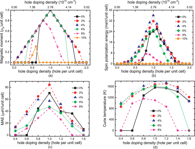
As mentioned above, the monolayer is a non-magnetic semiconductor with zero doping (, where is the hole doping density). However, our first-principles calculations show that the system develops a spontaneous FM phase via hole doping. In Fig. 3(a), we plot the magnetic moment versus the hole doping density. One clearly sees that ferromagnetism is obtained at a doping density (0.7 holes per unit cell). The magnetic moment of monolayer increases linearly as a function of the hole doping density. At the doping density (1 hole per unit cell), the magnetic moment reaches maximum . The magnetic moment is /holes in a wide hole doping range from to , which indicates that the holes are completely spin polarized, namely the spin polarization of holes is . However, the magnetic moment decreases linearly with continually increasing hole doping density , and the monolayer becomes non-magnetic phase at hole doping density larger than (1.6 holes per unit cell). The large DOS not only results in magnetic instability but also gives rise to structural distortions. We relax structure by optimizing the lattice constants and the atomic positions under different hole doping density. The results (seen the Table S2 in the Supplemental Material) indicate that the relaxed structure is little different from the undoped one. We also consider the electron doping effect. The electron doping can also introduce magnetic moment, however, it fluctuates with electron doping density (see Figure S2 in the Supplemental Material). This indicates the electron doped system has no stable obvious magnetic moment compared to the hole doped system. To illustrates the stability of ferromagnetism, we calculate the spin polarization energy of the system versus the hole doping density. Here, the spin polarization energy is defined as the energy difference between the non-spin-polarized and FM phases. We also test the several antiferromagnetic phases, and we find that the antiferromagnetic phases finally converge to non-magnetic phase. Fig. 3(b) shows that the polarization energy increases monotonically and it reaches the maximum (24.1 meV per hole) at the doping density , which is larger than those of (1.4 meV per carrier), (7.0 meV per carrier) and monolayer (8.5 meV per carrier), indicating its superiority for spintronics. After the doping density , the spin polarization energy decreases versus the doping density and drops to zero above .
The physical origin of ferromagnetism can be explained by the Stoner picture[51]. The system would develop ferromagnetism spontaneously when the Stoner criterion is satisfied, where the is Stoner interaction parameter defined as ( is the spin splitting energy and is the magnetic moment) and is the DOS at the Fermi level of the non-spin-polarized phase band structure. Hole doping increases and may introduce magnetism due to the large DOS near the valence band edges. In our calculations, we find that the Stoner criterion is larger than 1 in a wide hole doping range from to . When the hole concentration is not in this range, is not large enough and the Stoner criterion is not satisfied, thus the system is nonmagnetic. For instance, in the case of the hole doping density , the spin splitting eV and the per unit cell, so the interaction parameter is about 0.37 eV/. The required DOS at the Fermi level to satisfy the Stone criterion is . The value of the DOS can reach (Figure S3 in the Supplemental Material), which is sufficiently large to develop ferromagnetism.
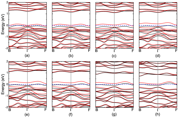
The band structures of monolayer under different hole doping density are displayed in Fig. 4. The calculated results suggest that the monolayer becomes a HM with minority-spin bands being metal characteristic and majority-spin bands being semiconductor characteristic when the hole doping density is larger than , as shown in Fig. 4(a). The spin splitting near the Fermi level increases with increasing the hole doping density and gets to its maximum at the hole doping density (Fig.4(d)), and the monolayer becomes a FM spin gapless semiconductor. Subsequently, the spin splitting decreases with increasing hole doping density, and half-metallicity of the system reproduces but with an inverse spin-polarization direction (minority-spin bands exhibit semiconductor characteristic and majority-spin bands exhibit metal characteristic) (Figs. 4(e)-(h)). Finally, the spin splitting vanishes when the hole doping density is larger than . The reversible spin polarization[52, 53] provides a feasible method for manipulation of spin-polarized currents and hold many advantages in spintronic application. The monolayer shows ferromagnetism over a significant wide range of hole doping density, from to , which is larger than that of previously reported in ( to (0.09 to 0.78 electron per unit cell)). Moreover, the monolayer exhibits half-metallicity over the whole range of hole doping density considered. However, half-metallicity of monolayer is observed at electron doping density from to . The excellent half-metallicity makes monolayer a promising candidate for spintronic applications.
To confirm the hole-doped monolayer is indeed HM, we also calculate the electronic structure and magnetic moment under the hole doping density (0.8 hole per unit cell) at HSE level. It is found that the magnetic moment is also , namely, the holes are fully spin polarized, which is same to that of PBE level. The DOS at HSE level (Figure S4 in the Supplemental Material) also shows the system is half-metallic phase with half-metallic gap 0.48 eV, which indicates that the half-metallicity of monolayer could be preserved from thermally agitated spin-flip transition.
The MAE not only reveals the ground-state magnetization orientation of system, but also indicates the relative stability of the long-range ferromagnetism against thermal excitation at finite temperatures[14]. In this work, we calculate the MAE including the spin-orbit coupling. The MAE is defined as , where the or is the total energy of hole-doped monolayer when the easy axis is along the out-of-plane () or the lowest in plane () orientation. The MAE as a function of hole doping density is shown in Fig. 3(c). It is found that the MAE can reach its maximum of 70.33 eV per hole for the hole doping density . This is much larger than that of monolayer (32 eV per hole)[35]. Considering the MAE per area, the hole-doped monolayer has a value of 3.72. The value is much smaller than that of (219)[54], but comparable to (3.2-21.1)[55] and (12.96)[56]. The comparison suggests that the hole-doped monolayer could be a useful materials in long-distance spin transport.
Here, we use the mean field method to estimate the of the hole-doped monolayer. At the mean field level, the magnetic moment can be estimated by minimizing the electronic free energy of the system at finite temperatures[35, 26, 57]. The effect of increasing temperature is simulated by changing the Gauss smearing factor (). We take doping density as an example to calculate the temperature-dependent magnetic moment(see Figure S5 in the Supplemental Material), which yield a critical exponent of 0.5 for the magnetic moment. By fitting the calculated magnetic moment squared to a linear function of temperature near the phase transition regime, we get an estimation of . The calculated as a function of hole doping density is presented in Fig.3(d). We find that the is higher than 800 K when the hole doing density is larger than , the maximum of can be up to 1557 K at the hole doping density . These are much higher than those of GaSe (about 90 K) and monolayer (about 320 K). One should be cautions that the mean field method tends to overestimate the . The values from mean field method could be modified with the empirical relation[58] (seen Figure S6 in the Supplemental Material for more details). The modified results indicate that the is still higher room temperature.
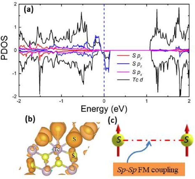

To clearly understand the physical origin of the high-temperature ferromagnetism and half-metallicity near the Fermi level in the hole-doped monolayer, we take the hole doping density as an example. The calculated PDOS (Fig. 5(a)) shows that the electronic states near the Fermi level are mainly derived from the orbital of S atoms inter the Tc chains. Thus, it is concluded that the magnetic moment of the hole-doped monolayer is mainly contributed by the partially occupied oribital of S atoms. Furthermore, the spin density distribution (Fig. 5(b)) also suggests that the magnetism mainly originates from S atoms inter the Tc chains. Therefore, a strong - coupling interaction is dominated around the Fermi level, which is different from the reported half-metallic one-dimensional metal-benzenetetramine ( coupling)[59]. Benefiting from the spatially extended feature of S- orbitals, the - direct exchange interaction (see Fig. 5(c)) is extended and thus results in a strong long-range FM coupling, which can be preserved against the thermal disturbance at high temperature.
3.3 The effect of biaxial tensile strain
Lattice strain is also an effective method to tune the magnetic properties of 2D materials. Hence, we study the strain-dependent magnetic properties of the hole-doped monolayer. In the present work, we only consider the biaxial tensile strain. Actually, it is reported that a critical tensile strain is larger than in monolayer [60]and graphene, phosphorene can sustain tensile strain above [61, 62]. The monolayer can sustain a critical strain of [41]. Below the point, the strained monolayer can return to its original geometry when the tensile strain is released. In Fig. 3(a), we plot the magnetic moment as a function of hole density under various biaxial tensile strain. It is observed that the hole density range for FM half-metallicity substantially increases with small tensile strain. For and tensile strain cases, the range is from 0 to (1.8 holes per unit cell) and from 0 to , respectively, which are much larger than that of zero strain (from to ). However, the range will decrease with larger tensile strain. For the and tensile strain cases, the range is from to and from to , respectively. When the tensile strain reaches , the magnetism is almost suppressed. In Figs. 3(b)-(d), we also plot the calculated spin polarization energy, MAE and versus hole doping density in different strain. A similar trend is observed in the maximal spin polarization energy, MAE and with different strain. These results imply that the strain is a powerful alternative method to tune the magnetism in the monolayer.
In order to understand the strain-dependent magnetism, we plot the band structure of the monolayer without hole doping under different tensile strain in Fig. 6. The band extremum along the -B (circled by the purple line) is gradually lowered with increasing the tensile strain, while the band at B point (circled by the purple line) is elevated gradually, and the band extremum along -F (circled by the green line) is elevated gradually. This leads to the valence band along -B near the Fermi level slowly becoming flat with small tensile strain, subsequently becoming dispersed with continuously increasing strain. However, the band along -F always is dispersed with increasing strain. As a result, the DOS at VBM is first increased, subsequently decreased with increasing strain, then the Stoner Criterion, , gets satisfied easily, and then satisfied hardly. According to the Stoner model, the ferromagnetism is first enhanced, subsequently reduced under hole doping, which is consistent with the discussion above.
3.4 Magnetism of the bilayer with hole doping
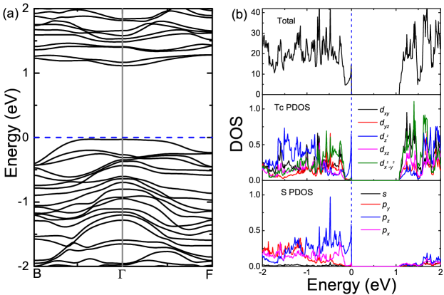
The bilayer is stacked along the -axis with AA-stacking order. The lattice constants ( and Å) are slightly smaller than the ones calculated for the monolayer. Specifically, the VBM of bilayer is switched to point, displaying a direct gap semiconductor, and the band gap decreases slightly to 1.13 eV, as shown in Fig. 7(a), which is consistent with the previous result[41]. The changes indicate that the interlayer interaction plays an important role on both geometrical structure and electronic behaviors. In addition, the flat dispersion of VBM is also observed in bilayer, and a large van Hove singularity characteristic DOS is observed at the VBM (Figs. 7(a) and 7(b)). Different from the monolayer, the contribution of Tc orbital in the VBM dominates over Tc orbital in the bilayer, and the peak at the energy of about -0.56 eV is vanished. Moreover, the peak of S atoms near the Fermi level is also shifted from -0.22 eV to -0.006 eV. These results indicate that of Tc atoms and of S atoms electrons energy is increased when the bilayer introduces the interlayer interaction. In other words, the and electrons states become less stable with interlayer interaction.
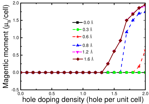
As suggested above, it is expected that the bilayer would develop ferromagnetism under hole doping because of the large DOS with van Hove singularity characteristic at the energy of 0.0016 eV below the Fermi level. To examine the concept, we calculate magnetic moment as a function of hole doping density for the bilayer and present it in Fig. 8. However, the system does not exhibit magnetism under hole doping. In order to investigate whether the interlayer interaction has effect on magnetism of the nanosheet, in Fig. 8, we show the hole-dependent magnetic moment after expanding the layer separation. The magnetism appear at the layer expansion of 0.6 Å and the spin polarization of hole nearly reach saturation at the layer expansion of 1.6 Å. According to this, we conclude that the interlayer interactions have significant effect on magnetism. Since the interlayer interaction contains VDW forces and interlayer electron interaction, the two cases should be considered separately. Firstly, we test the simulation without involving VDW forces. It is found that the layer separation is shrunk by 0.8 Å with VDW forces in the DFT-D2 approximation. Thus, we set the layer separation equivalent to expansion of the layer separation (by 0.8 Å), and calculate the magnetic moment with hole doping before and after removing the DFT-D2 approximation. If VDW forces is crucial to the magnetic behavior, the magnetism should be enhanced after removing the DFT-D2 approximation. However, this do not occur in our calculation. Therefore, we conclude that the interlayer VDW forces hardly affect the formation of ferromagnetism in the bilayer. So the interlayer electron interaction is responsible for the phenomenon.
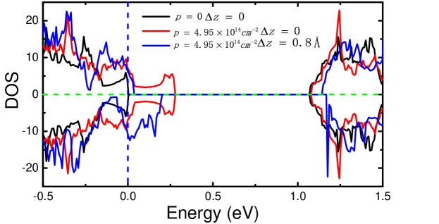
To further study how the interlayer interaction affects the magnetic properties in the system, we plot the DOS of pristine bilayer and that with hole doping (, before and after layer separation expansion of 0.8Å). As displayed in Fig. 9, the hole doping (the red curves) make the VBM move towards the higher-energy level by 0.28 eV and the Fermi level crosses the valence band. On the other hand, the CBM also shifts slightly to high-energy level by 0.016 eV. However, there is no exchange splitting between the majority-spin and minority-spin channel, and the DOS curves is symmetrical. After expanding the layer separation by 0.8 Å, as shown in Fig. 9, the hole doping (the blue curves) makes minority-spin channel shift towards high-energy level by 0.204 eV, and 0.035 eV for the majority-spin channel. The exchange splitting of the two spin channel is 0.169 eV, indicating that the breaking of time symmetry, namely resulting in reproducing ferromagnetism in the system. The reappearance of magnetism suggests that the interlayer interaction is important to develop ferromagnetism for the nanosheets. Based on the band-structure analysis, the flat dispersion of VBM are retained for the bilayer. This indicates that the flat band structure (large DOS at or near the Fermi level) can not guarantee the formation of ferromagnetism for the bilayer, namely, breaking of the time symmetry.
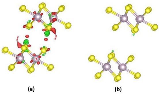
We obtain the charge density difference by subtracting the single layer’s charge density from that of the bilayer for the pristine bilayer and layer separation expansion (0.8 Å) and display them in Fig. 10. As show clearly, for the pristine bilayer, the electrons at the inner S atoms are depleted and the electrons are accumulated within the interlayer space. However, the electrons depletion and accumulation is hardly observed for the case of layer separation expansion. The phenomenon indicates that electrons transfer between layers due to the formation of multilayers. The behavior of interlayer electrons suggests that the interlayer electron interacton is closely correlated to the magnetic coupling. The hybridization of electron wave function is reduced with increasing the layer separation. Therefore, the ferromagnetism reappears upon hole doping. As discussed above, we conclude that the accumulated interlayer electrons can suppress the FM coupling in the hole-doped bilayer. It was also reported that the ferromagnetism in the SnO bilayer depending on the balance of interlayer lone-pair electron interaction and the hole doping[63]
3.5 Discussion
Although our work provides a general way to obtain high-temperature ferromagnetism and robust half-metallicity based on the monolayer, it is necessary to discuss several points in the following: (i) The possibility to obtain monolayer is tested by using two computational strategies[41]. One is to calculate the formation energy , which determines the strength of the interlayer van der Waals interaction in the bulk. The of monolayer is estimated to 76 meV, which is smaller than that of monolayer (94 meV), and comparable to that of monolayer (77 meV)[64], indicating the easy of extracting single-layer from the bulk form. The other route is to exfoliate the sigle-layer from bulk and estimate the cleavage energy . The calculated of monolayer is smaller that of monolayer and analogous to that of graphite. Given the monolayer and graphene have been successfully exfoliated, it is expected that the same should be successful for the monolayer. The dynamical and thermal stabilities of the monolayer are also confirmed by calculating phonon dispersion and ab initio molecular dynamics (AIMD) simulations with PBE functional (see Figure S7 in the Supplemental Material). (ii) The hole doping density can be tuned by the gating technique. For instance, the carrier doping density can reach the order of in graphene by ion liquid gating[65], and the order of in dichalcogenide monolayer by back-gate gating[66], even the order of by electrolyte gating[67]. (iii) In according to the Mermin-Wagner theorem, a 2D Heisenberg system does not exist long-range magnetic order at finite temperature[68]. However, the hypothesis of the theorem can be broken due to the magnetic anisotropy[69] which can stabilize the magnetic order in a finite size and temperature. So it is expected that the half metallicity produced by hole doping in the monolayer can be accessible experimentally.
4 CONCLUSIONS
In conclusion, we show that the -orbital half-metallicity can be introduced when hole are doped into the monolayer from first principles calculation. The half-metallic phase with tunable spin-polarization orientation can be achieved in a wide range of hole doping density from to . Moreover, the half-metallicity is confirmed with the HSE06 method. The strong - direct exchange interaction is responsible for a FM phsae with above room temperature. Additionally, the lattice strain is an effective way to tune magnetism. A similar reversible modulation of magnetic moments and electronic phase transitions between half-metallic and semiconducting phases in zigzag nanoribbons has also been revealed[70]. The monolayer is considered to be promising candidate for spintronic application due to experimental feasible synthesis, robust -orbital FM half-metallicity and high . In the bilayer, the ferromagnetism depends on not only the hole doping density but also the interlayer interaction. In this work, we pave a way for exploring the nanoscale magnetism for spintronic applications and provide a comprehensive picture for the mechanism of the magnetic behavior in the nanosheets.
Conflicts of interest
There are no conflicts to declare.
Acknowledgements
The authors thank Yijie Zeng and Wanxing Lin for helpful discussions. This project is supported by NKRDPC-2017YFA0206203, NKRDPC-2018YFA0306001, NSFC-11574404, NSFG-2015A030313176, the National Supercomputer Center in Guangzhou, Three Big Constructions-Supercomputing Application Cultivation Projects, and the Leading Talent Program of Guangdong Special Projects.
References
References
-
[1]
D. Xiao, G.-B. Liu, W. Feng, X. Xu, W. Yao,
Coupled spin
and valley physics in monolayers of and other group-vi
dichalcogenides, Phys. Rev. Lett. 108 (2012) 196802.
doi:10.1103/PhysRevLett.108.196802.
URL https://link.aps.org/doi/10.1103/PhysRevLett.108.196802 -
[2]
M. Ezawa, A topological
insulator and helical zero mode in silicene under an inhomogeneous electric
field, New J. Phys. 14 (3) (2012) 033003.
URL http://stacks.iop.org/1367-2630/14/i=3/a=033003 -
[3]
A. Kormányos, V. Zólyomi, N. D. Drummond, P. Rakyta, G. Burkard, V. I.
Fal’ko, Monolayer
mos2: Trigonal warping, the valley, and
spin-orbit coupling effects, Phys. Rev. B 88 (2013) 045416.
doi:10.1103/PhysRevB.88.045416.
URL https://link.aps.org/doi/10.1103/PhysRevB.88.045416 -
[4]
S. Lebègue, T. Björkman, M. Klintenberg, R. M. Nieminen, O. Eriksson,
Two-dimensional
materials from data filtering and ab initio calculations, Phys. Rev. X 3
(2013) 031002.
doi:10.1103/PhysRevX.3.031002.
URL https://link.aps.org/doi/10.1103/PhysRevX.3.031002 -
[5]
J. N. Coleman, M. Lotya, A. O’Neill, S. D. Bergin, P. J. King,
U. Khan, K. Young, A. Gaucher, S. De, R. J. Smith, I. V. Shvets, S. K. Arora,
G. Stanton, H.-Y. Kim, K. Lee, G. T. Kim, G. S. Duesberg, T. Hallam, J. J.
Boland, J. J. Wang, J. F. Donegan, J. C. Grunlan, G. Moriarty, A. Shmeliov,
R. J. Nicholls, J. M. Perkins, E. M. Grieveson, K. Theuwissen, D. W. McComb,
P. D. Nellist, V. Nicolosi,
Two-dimensional
nanosheets produced by liquid exfoliation of layered materials, Science
331 (6017) (2011) 568–571.
arXiv:http://science.sciencemag.org/content/331/6017/568.full.pdf,
doi:10.1126/science.1194975.
URL http://science.sciencemag.org/content/331/6017/568 -
[6]
P. Vogt, P. De Padova, C. Quaresima, J. Avila, E. Frantzeskakis, M. C. Asensio,
A. Resta, B. Ealet, G. Le Lay,
Silicene:
Compelling experimental evidence for graphenelike two-dimensional silicon,
Phys. Rev. Lett. 108 (2012) 155501.
doi:10.1103/PhysRevLett.108.155501.
URL https://link.aps.org/doi/10.1103/PhysRevLett.108.155501 -
[7]
J. Lee, W.-C. Tian, W.-L. Wang, D.-X. Yao,
Two-dimensional pnictogen
honeycomb lattice: Structure, on-site spin-orbit coupling and spin
polarization, Sci. Rep. 5 (2015) 11512.
doi:10.1038/srep11512.
URL http://dx.doi.org/10.1038/srep11512 -
[8]
Y. C. Cheng, Z. Y. Zhu, W. B. Mi, Z. B. Guo, U. Schwingenschlögl,
Prediction of
two-dimensional diluted magnetic semiconductors: Doped monolayer mos2
systems, Phys. Rev. B 87 (2013) 100401.
doi:10.1103/PhysRevB.87.100401.
URL https://link.aps.org/doi/10.1103/PhysRevB.87.100401 -
[9]
G. Gao, G. Ding, J. Li, K. Yao, M. Wu, M. Qian,
Monolayer mxenes: promising
half-metals and spin gapless semiconductors, Nanoscale 8 (2016) 8986–8994.
doi:10.1039/C6NR01333C.
URL http://dx.doi.org/10.1039/C6NR01333C -
[10]
K. J. Saji, K. Tian, M. Snure, A. Tiwari,
2d tin
monoxide an unexplored p-type van der waals semiconductor: Material
characteristics and field effect transistors, Advanced Electronic Materials
2 (4) 1500453.
arXiv:https://onlinelibrary.wiley.com/doi/pdf/10.1002/aelm.201500453,
doi:10.1002/aelm.201500453.
URL https://onlinelibrary.wiley.com/doi/abs/10.1002/aelm.201500453 -
[11]
Q. H. Wang, K. Kalantar-Zadeh, A. Kis, J. N. Coleman, M. S. Strano,
Electronics and
optoelectronics of two-dimensional transition metal dichalcogenides, Nature
Nanotechnology 7 (2012) 699.
doi:10.1038/nnano.2012.193.
URL http://dx.doi.org/10.1038/nnano.2012.193 -
[12]
K. S. Novoselov, A. K. Geim, S. V. Morozov, D. Jiang, Y. Zhang, S. V. Dubonos,
I. V. Grigorieva, A. A. Firsov,
Electric field
effect in atomically thin carbon films, Science 306 (5696) (2004) 666–669.
arXiv:http://science.sciencemag.org/content/306/5696/666.full.pdf,
doi:10.1126/science.1102896.
URL http://science.sciencemag.org/content/306/5696/666 -
[13]
C. Lee, Q. Li, W. Kalb, X.-Z. Liu, H. Berger, R. W. Carpick, J. Hone,
Frictional
characteristics of atomically thin sheets, Science 328 (5974) (2010) 76–80.
arXiv:http://science.sciencemag.org/content/328/5974/76.full.pdf,
doi:10.1126/science.1184167.
URL http://science.sciencemag.org/content/328/5974/76 -
[14]
B. Huang, G. Clark, E. Navarro-Moratalla, D. R. Klein, R. Cheng, K. L. Seyler,
D. Zhong, E. Schmidgall, M. A. McGuire, D. H. Cobden, W. Yao, D. Xiao,
P. Jarillo-Herrero, X. Xu,
Layer-dependent ferromagnetism
in a van der waals crystal down to the monolayer limit, Nature 546 (2017)
270.
doi:10.1038/nature22391.
URL http://dx.doi.org/10.1038/nature22391 -
[15]
C. Gong, L. Li, Z. Li, H. Ji, A. Stern, Y. Xia, T. Cao, W. Bao, C. Wang,
Y. Wang, Z. Q. Qiu, R. J. Cava, S. G. Louie, J. Xia, X. Zhang,
Discovery of intrinsic
ferromagnetism in two-dimensional van der waals crystals, Nature 546 (2017)
265.
doi:10.1038/nature22060.
URL http://dx.doi.org/10.1038/nature22060 -
[16]
B. Wang, Q. Wu, Y. Zhang, Y. Guo, X. Zhang, Q. Zhou, S. Dong, J. Wang,
High curie-temperature intrinsic
ferromagnetism and hole doping-induced half-metallicity in two-dimensional
scandium chlorine monolayers, Nanoscale Horiz. 3 (2018) 551–555.
doi:10.1039/C8NH00101D.
URL http://dx.doi.org/10.1039/C8NH00101D -
[17]
M. Bonilla, S. Kolekar, Y. Ma, H. C. Diaz, V. Kalappattil, R. Das, T. Eggers,
H. R. Gutierrez, M.-H. Phan, M. Batzill,
Strong room-temperature
ferromagnetism in vse2 monolayers on van der waals substrates, Nature
Nanotechnology 13 (4) (2018) 289–293.
doi:10.1038/s41565-018-0063-9.
URL https://doi.org/10.1038/s41565-018-0063-9 -
[18]
A. Ramasubramaniam, D. Naveh,
Mn-doped monolayer
mos2: An atomically thin dilute magnetic semiconductor, Phys. Rev. B
87 (2013) 195201.
doi:10.1103/PhysRevB.87.195201.
URL https://link.aps.org/doi/10.1103/PhysRevB.87.195201 -
[19]
K. Pi, K. M. McCreary, W. Bao, W. Han, Y. F. Chiang, Y. Li, S.-W. Tsai, C. N.
Lau, R. K. Kawakami,
Electronic doping
and scattering by transition metals on graphene, Phys. Rev. B 80 (2009)
075406.
doi:10.1103/PhysRevB.80.075406.
URL https://link.aps.org/doi/10.1103/PhysRevB.80.075406 -
[20]
B. Huang, H. Xiang, J. Yu, S.-H. Wei,
Effective
control of the charge and magnetic states of transition-metal atoms on
single-layer boron nitride, Phys. Rev. Lett. 108 (2012) 206802.
doi:10.1103/PhysRevLett.108.206802.
URL https://link.aps.org/doi/10.1103/PhysRevLett.108.206802 -
[21]
A. V. Krasheninnikov, P. O. Lehtinen, A. S. Foster, P. Pyykkö, R. M.
Nieminen,
Embedding
transition-metal atoms in graphene: Structure, bonding, and magnetism, Phys.
Rev. Lett. 102 (2009) 126807.
doi:10.1103/PhysRevLett.102.126807.
URL https://link.aps.org/doi/10.1103/PhysRevLett.102.126807 -
[22]
Y. Yang, M. Guo, G. Zhang, W. Li,
Tuning
the electronic and magnetic properties of porous graphene-like carbon nitride
through 3d transition-metal doping, Carbon 117 (2017) 120 – 125.
doi:https://doi.org/10.1016/j.carbon.2017.02.069.
URL http://www.sciencedirect.com/science/article/pii/S0008622317301999 -
[23]
S. Zhang, R. Chi, C. Li, Y. Jia,
Structural,
electronic and magnetic properties of 3d transition metals embedded
graphene-like carbon nitride sheet: A dft + u study, Physics Letters A
380 (14) (2016) 1373 – 1377.
doi:https://doi.org/10.1016/j.physleta.2016.01.051.
URL http://www.sciencedirect.com/science/article/pii/S0375960116000943 -
[24]
J. Du, C. Xia, W. Xiong, X. Zhao, T. Wang, Y. Jia,
Tuning the electronic structures
and magnetism of two-dimensional porous c2n via transition metal embedding,
Phys. Chem. Chem. Phys. 18 (2016) 22678–22686.
doi:10.1039/C6CP03210A.
URL http://dx.doi.org/10.1039/C6CP03210A -
[25]
E.-j. Kan, Z. Li, J. Yang, J. G. Hou,
Half-metallicity in edge-modified
zigzag graphene nanoribbons, Journal of the American Chemical Society
130 (13) (2008) 4224–4225, pMID: 18331034.
arXiv:https://doi.org/10.1021/ja710407t, doi:10.1021/ja710407t.
URL https://doi.org/10.1021/ja710407t -
[26]
T. Cao, Z. Li, S. G. Louie,
Tunable
magnetism and half-metallicity in hole-doped monolayer gase, Phys. Rev.
Lett. 114 (2015) 236602.
doi:10.1103/PhysRevLett.114.236602.
URL https://link.aps.org/doi/10.1103/PhysRevLett.114.236602 -
[27]
H. Sevin?li, Quartic
dispersion, strong singularity, magnetic instability, and unique
thermoelectric properties in two-dimensional hexagonal lattices of group-va
elements, Nano Letters 17 (4) (2017) 2589–2595, pMID: 28318269.
arXiv:https://doi.org/10.1021/acs.nanolett.7b00366, doi:10.1021/acs.nanolett.7b00366.
URL https://doi.org/10.1021/acs.nanolett.7b00366 -
[28]
E. V. Castro, N. M. R. Peres, T. Stauber, N. A. P. Silva,
Low-density
ferromagnetism in biased bilayer graphene, Phys. Rev. Lett. 100 (2008)
186803.
doi:10.1103/PhysRevLett.100.186803.
URL https://link.aps.org/doi/10.1103/PhysRevLett.100.186803 -
[29]
M. Zulfiqar, Y. Zhao, G. Li, S. Nazir, J. Ni,
Tunable conductivity and half
metallic ferromagnetism in monolayer platinum diselenide: A first-principles
study, The Journal of Physical Chemistry C 120 (43) (2016) 25030–25036.
arXiv:https://doi.org/10.1021/acs.jpcc.6b06999, doi:10.1021/acs.jpcc.6b06999.
URL https://doi.org/10.1021/acs.jpcc.6b06999 -
[30]
N. Miao, B. Xu, N. C. Bristowe, J. Zhou, Z. Sun,
Tunable magnetism and
extraordinary sunlight absorbance in indium triphosphide monolayer, Journal
of the American Chemical Society 139 (32) (2017) 11125–11131, pMID:
28731338.
arXiv:https://doi.org/10.1021/jacs.7b05133, doi:10.1021/jacs.7b05133.
URL https://doi.org/10.1021/jacs.7b05133 -
[31]
S. Gong, W. Wan, S. Guan, B. Tai, C. Liu, B. Fu, S. A. Yang, Y. Yao,
Tunable half-metallic magnetism
in an atom-thin holey two-dimensional c2n monolayer, J. Mater. Chem. C 5
(2017) 8424–8430.
doi:10.1039/C7TC01399J.
URL http://dx.doi.org/10.1039/C7TC01399J -
[32]
Z. Liang, B. Xu, H. Xiang, Y. Xia, J. Yin, Z. Liu,
Carrier-tunable magnetism in two
dimensional graphene-like c2n, RSC Adv. 6 (2016) 54027–54031.
doi:10.1039/C6RA08254H.
URL http://dx.doi.org/10.1039/C6RA08254H -
[33]
L. Seixas, A. S. Rodin, A. Carvalho, A. H. Castro Neto,
Multiferroic
two-dimensional materials, Phys. Rev. Lett. 116 (2016) 206803.
doi:10.1103/PhysRevLett.116.206803.
URL https://link.aps.org/doi/10.1103/PhysRevLett.116.206803 -
[34]
C.-W. Wu, J.-H. Huang, D.-X. Yao,
Tunable
room-temperature ferromagnetism in the sic monolayer, Journal of Magnetism
and Magnetic Materials 469 (2019) 306 – 314.
doi:https://doi.org/10.1016/j.jmmm.2018.08.054.
URL http://www.sciencedirect.com/science/article/pii/S0304885318316858 -
[35]
S.-H. Zhang, B.-G. Liu,
Hole-doping-induced half-metallic
ferromagnetism in a highly-air-stable pdse2 monolayer under uniaxial stress,
J. Mater. Chem. C 6 (2018) 6792–6798.
doi:10.1039/C8TC01450G.
URL http://dx.doi.org/10.1039/C8TC01450G -
[36]
B. Sipos, A. F. Kusmartseva, A. Akrap, H. Berger, L. Forr , E. Tuti?,
From mott state to
superconductivity in?1t-tas2, Nature Materials 7 (2008) 960.
doi:10.1038/nmat2318.
URL http://dx.doi.org/10.1038/nmat2318 -
[37]
A. H. Castro Neto,
Charge density
wave, superconductivity, and anomalous metallic behavior in 2d transition
metal dichalcogenides, Phys. Rev. Lett. 86 (2001) 4382–4385.
doi:10.1103/PhysRevLett.86.4382.
URL https://link.aps.org/doi/10.1103/PhysRevLett.86.4382 -
[38]
J. Wilson, F. D. Salvo, S. Mahajan,
Charge-density waves and
superlattices in the metallic layered transition metal dichalcogenides,
Advances in Physics 24 (2) (1975) 117–201.
arXiv:https://doi.org/10.1080/00018737500101391, doi:10.1080/00018737500101391.
URL https://doi.org/10.1080/00018737500101391 -
[39]
M. N. Ali, J. Xiong, S. Flynn, J. Tao, Q. D. Gibson, L. M. Schoop, T. Liang,
N. Haldolaarachchige, M. Hirschberger, N. P. Ong, R. J. Cava,
Large, non-saturating
magnetoresistance in wte2, Nature 514 (2014) 205.
doi:10.1038/nature13763.
URL http://dx.doi.org/10.1038/nature13763 -
[40]
E. Liu, Y. Fu, Y. Wang, Y. Feng, H. Liu, X. Wan, W. Zhou, B. Wang, L. Shao,
C.-H. Ho, Y.-S. Huang, Z. Cao, L. Wang, A. Li, J. Zeng, F. Song, X. Wang,
Y. Shi, H. Yuan, H. Y. Hwang, Y. Cui, F. Miao, D. Xing,
Integrated digital inverters
based on two-dimensional anisotropic res2 field-effect transistors, Nature
Communications 6 (2015) 6991.
doi:10.1038/ncomms7991%****␣TcS2_revised_MAGMA_2018_3536.bbl␣Line␣400␣****https://www.nature.com/articles/ncomms7991#supplementary-information.
URL http://dx.doi.org/10.1038/ncomms7991 -
[41]
Y. Jiao, L. Zhou, F. Ma, G. Gao, L. Kou, J. Bell, S. Sanvito, A. Du,
Predicting single-layer
technetium dichalcogenides (tcx2, x = s, se) with promising applications in
photovoltaics and photocatalysis, ACS Applied Materials & Interfaces 8 (8)
(2016) 5385–5392, pMID: 26859697.
arXiv:https://doi.org/10.1021/acsami.5b12606, doi:10.1021/acsami.5b12606.
URL https://doi.org/10.1021/acsami.5b12606 -
[42]
G. Kresse, D. Joubert,
From ultrasoft
pseudopotentials to the projector augmented-wave method, Phys. Rev. B 59
(1999) 1758–1775.
doi:10.1103/PhysRevB.59.1758.
URL https://link.aps.org/doi/10.1103/PhysRevB.59.1758 -
[43]
G. Kresse, J. Hafner,
Ab initio
molecular-dynamics simulation of the liquid-metal–amorphous-semiconductor
transition in germanium, Phys. Rev. B 49 (1994) 14251–14269.
doi:10.1103/PhysRevB.49.14251.
URL https://link.aps.org/doi/10.1103/PhysRevB.49.14251 -
[44]
P. E. Blöchl,
Projector
augmented-wave method, Phys. Rev. B 50 (1994) 17953–17979.
doi:10.1103/PhysRevB.50.17953.
URL https://link.aps.org/doi/10.1103/PhysRevB.50.17953 -
[45]
J. P. Perdew, K. Burke, M. Ernzerhof,
Generalized
gradient approximation made simple, Phys. Rev. Lett. 77 (1996) 3865–3868.
doi:10.1103/PhysRevLett.77.3865.
URL https://link.aps.org/doi/10.1103/PhysRevLett.77.3865 -
[46]
J. Heyd, G. E. Scuseria, M. Ernzerhof,
Hybrid functionals based on a
screened coulomb potential, The Journal of Chemical Physics 118 (18) (2003)
8207–8215.
arXiv:https://doi.org/10.1063/1.1564060, doi:10.1063/1.1564060.
URL https://doi.org/10.1063/1.1564060 -
[47]
P. F. Weck, E. Kim, K. R. Czerwinski,
Semiconducting layered technetium
dichalcogenides: insights from first-principles, Dalton Trans. 42 (2013)
15288–15295.
doi:10.1039/C3DT51903A.
URL http://dx.doi.org/10.1039/C3DT51903A -
[48]
H.-J. Lamfers, A. Meetsma, G. Wiegers, J. de Boer,
The
crystal structure of some rhenium and technetium dichalcogenides, Journal of
Alloys and Compounds 241 (1) (1996) 34 – 39.
doi:https://doi.org/10.1016/0925-8388(96)02313-4.
URL http://www.sciencedirect.com/science/article/pii/0925838896023134 -
[49]
X. Gonze, C. Lee,
Dynamical matrices,
born effective charges, dielectric permittivity tensors, and interatomic
force constants from density-functional perturbation theory, Phys. Rev. B 55
(1997) 10355–10368.
doi:10.1103/PhysRevB.55.10355.
URL https://link.aps.org/doi/10.1103/PhysRevB.55.10355 -
[50]
Y. Nie, M. Rahman, P. Liu, A. Sidike, Q. Xia, G.-h. Guo,
Room-temperature
half-metallicity in monolayer honeycomb structures of group-v binary
compounds with carrier doping, Phys. Rev. B 96 (2017) 075401.
doi:10.1103/PhysRevB.96.075401.
URL https://link.aps.org/doi/10.1103/PhysRevB.96.075401 - [51] E. C. Stoner, Collective electron ferromagnetism. ii. energy and specific heat, Proceedings of the Royal Society A Mathematical Physical and Engineering Sciences 169 (169) (1939) 339–371.
-
[52]
X. Li, X. Wu, Z. Li, J. Yang, J. G. Hou,
Bipolar magnetic semiconductors:
a new class of spintronics materials, Nanoscale 4 (2012) 5680–5685.
doi:10.1039/C2NR31743E.
URL http://dx.doi.org/10.1039/C2NR31743E -
[53]
S.-J. Gong, C. Gong, Y.-Y. Sun, W.-Y. Tong, C.-G. Duan, J.-H. Chu, X. Zhang,
Electrically induced 2d
half-metallic antiferromagnets and spin field effect transistors,
Proceedings of the National Academy of Sciences 115 (34) (2018) 8511–8516.
arXiv:http://www.pnas.org/content/115/34/8511.full.pdf, doi:10.1073/pnas.1715465115.
URL http://www.pnas.org/content/115/34/8511 -
[54]
P. Chen, J.-Y. Zou, B.-G. Liu,
Intrinsic ferromagnetism and
quantum anomalous hall effect in a cobr2 monolayer, Phys. Chem. Chem. Phys.
19 (2017) 13432–13437.
doi:10.1039/C7CP02158E.
URL http://dx.doi.org/10.1039/C7CP02158E -
[55]
H. L. Zhuang, Y. Xie, P. R. C. Kent, P. Ganesh,
Computational
discovery of ferromagnetic semiconducting single-layer
, Phys. Rev. B 92 (2015) 035407.
doi:10.1103/PhysRevB.92.035407.
URL https://link.aps.org/doi/10.1103/PhysRevB.92.035407 -
[56]
E. Torun, H. Sahin, C. Bacaksiz, R. T. Senger, F. M. Peeters,
Tuning the
magnetic anisotropy in single-layer crystal structures, Phys. Rev. B 92
(2015) 104407.
doi:10.1103/PhysRevB.92.104407.
URL https://link.aps.org/doi/10.1103/PhysRevB.92.104407 -
[57]
B. Fu, W. Feng, X. Zhou, Y. Yao,
Effects of hole doping
and strain on magnetism in buckled phosphorene and arsenene, 2D Materials
4 (2) (2017) 025107.
URL http://stacks.iop.org/2053-1583/4/i=2/a=025107 - [58] Zhifeng, Junyan, Jijun, Zhao, Yn2 monolayer novel p-state dirac half metal for high-speed spintronics, Nano Research 10 (6) (2017) 1972–1979.
-
[59]
Y. Wan, Y. Sun, X. Wu, J. Yang,
Ambipolar half-metallicity in
one-dimensional metal c(1,2,4,5-benzenetetramine) coordination polymers via
carrier doping, The Journal of Physical Chemistry C 122 (1) (2018) 989–994.
arXiv:https://doi.org/10.1021/acs.jpcc.7b12022, doi:10.1021/acs.jpcc.7b12022.
URL https://doi.org/10.1021/acs.jpcc.7b12022 -
[60]
S. Guan, Y. Cheng, C. Liu, J. Han, Y. Lu, S. A. Yang, Y. Yao,
Effects of strain on electronic and
optic properties of holey two-dimensional c2n crystals, Applied Physics
Letters 107 (23) (2015) 231904.
arXiv:https://doi.org/10.1063/1.4937269, doi:10.1063/1.4937269.
URL https://doi.org/10.1063/1.4937269 -
[61]
K. S. Kim, Y. Zhao, H. Jang, S. Y. Lee, J. M. Kim, K. S. Kim, J.-H. Ahn,
P. Kim, J.-Y. Choi, B. H. Hong,
Large-scale pattern growth of
graphene films for stretchable transparent electrodes, Nature 457 (2009)
706.
doi:10.1038/nature07719https://www.nature.com/articles/nature07719#supplementary-information.
URL http://dx.doi.org/10.1038/nature07719 -
[62]
X. Peng, Q. Wei, A. Copple,
Strain-engineered
direct-indirect band gap transition and its mechanism in two-dimensional
phosphorene, Phys. Rev. B 90 (2014) 085402.
doi:10.1103/PhysRevB.90.085402.
URL https://link.aps.org/doi/10.1103/PhysRevB.90.085402 -
[63]
L. Guan, J. Tao,
Mechanism of
magnetic coupling in carrier-doped sno nanosheets, Phys. Rev. Applied 8
(2017) 064019.
doi:10.1103/PhysRevApplied.8.064019.
URL https://link.aps.org/doi/10.1103/PhysRevApplied.8.064019 -
[64]
H. L. Zhuang, R. G. Hennig,
Computational search for
single-layer transition-metal dichalcogenide photocatalysts, The Journal of
Physical Chemistry C 117 (40) (2013) 20440–20445.
arXiv:https://doi.org/10.1021/jp405808a, doi:10.1021/jp405808a.
URL https://doi.org/10.1021/jp405808a -
[65]
D. K. Efetov, P. Kim,
Controlling
electron-phonon interactions in graphene at ultrahigh carrier densities,
Phys. Rev. Lett. 105 (2010) 256805.
doi:10.1103/PhysRevLett.105.256805.
URL https://link.aps.org/doi/10.1103/PhysRevLett.105.256805 -
[66]
Y. J. Zhang, T. Oka, R. Suzuki, J. T. Ye, Y. Iwasa,
Electrically
switchable chiral light-emitting transistor, Science 344 (6185) (2014)
725–728.
arXiv:http://science.sciencemag.org/content/344/6185/725.full.pdf,
doi:10.1126/science.1251329.
URL http://science.sciencemag.org/content/344/6185/725 -
[67]
X. Li, X. Wu, J. Yang,
Half-metallicity in mnpse3
exfoliated nanosheet with carrier doping, Journal of the American Chemical
Society 136 (31) (2014) 11065–11069, pMID: 25036853.
arXiv:https://doi.org/10.1021/ja505097m, doi:10.1021/ja505097m.
URL https://doi.org/10.1021/ja505097m -
[68]
N. D. Mermin, H. Wagner,
Absence of
ferromagnetism or antiferromagnetism in one- or two-dimensional isotropic
heisenberg models, Phys. Rev. Lett. 17 (1966) 1133–1136.
doi:10.1103/PhysRevLett.17.1133.
URL https://link.aps.org/doi/10.1103/PhysRevLett.17.1133 -
[69]
M. Bander, D. L. Mills,
Ferromagnetism of
ultrathin films, Phys. Rev. B 38 (1988) 12015–12018.
doi:10.1103/PhysRevB.38.12015.
URL https://link.aps.org/doi/10.1103/PhysRevB.38.12015 -
[70]
L. Kou, C. Tang, Y. Zhang, T. Heine, C. Chen, T. Frauenheim,
Tuning magnetism and electronic
phase transitions by strain and electric field in zigzag mos2 nanoribbons,
The Journal of Physical Chemistry Letters 3 (20) (2012) 2934–2941, pMID:
26292229.
arXiv:https://doi.org/10.1021/jz301339e, doi:10.1021/jz301339e.
URL https://doi.org/10.1021/jz301339e