Electronically enhanced layer buckling and Au-Au dimerization in epitaxial LaAuSb films
Abstract
We report the molecular beam epitaxial growth, structure, and electronic measurements of single-crystalline LaAuSb films on Al2O3 (0001) substrates. LaAuSb belongs to a broad family of hexagonal intermetallics in which the magnitude and sign of layer buckling have strong effects on properties, e.g., predicted hyperferroelecticity, polar metallicity, and Weyl and Dirac states. Scanning transmission electron microscopy reveals highly buckled planes of Au-Sb atoms, with strong interlayer Au-Au interactions and a doubling of the unit cell. This buckling is four times larger than the buckling observed in other s with similar composition, e.g. LaAuGe and LaPtSb. Photoemission spectroscopy measurements and comparison with theory suggest an electronic driving force for the Au-Au dimerization, since LaAuSb, with a 19-electron count, has one more valence electron per formula unit than most stable s. Our results suggest that the electron count, in addition to conventional parameters such as epitaxial strain and chemical pressure, provides a powerful means for tuning the layer buckling in ferroic s.
pacs:
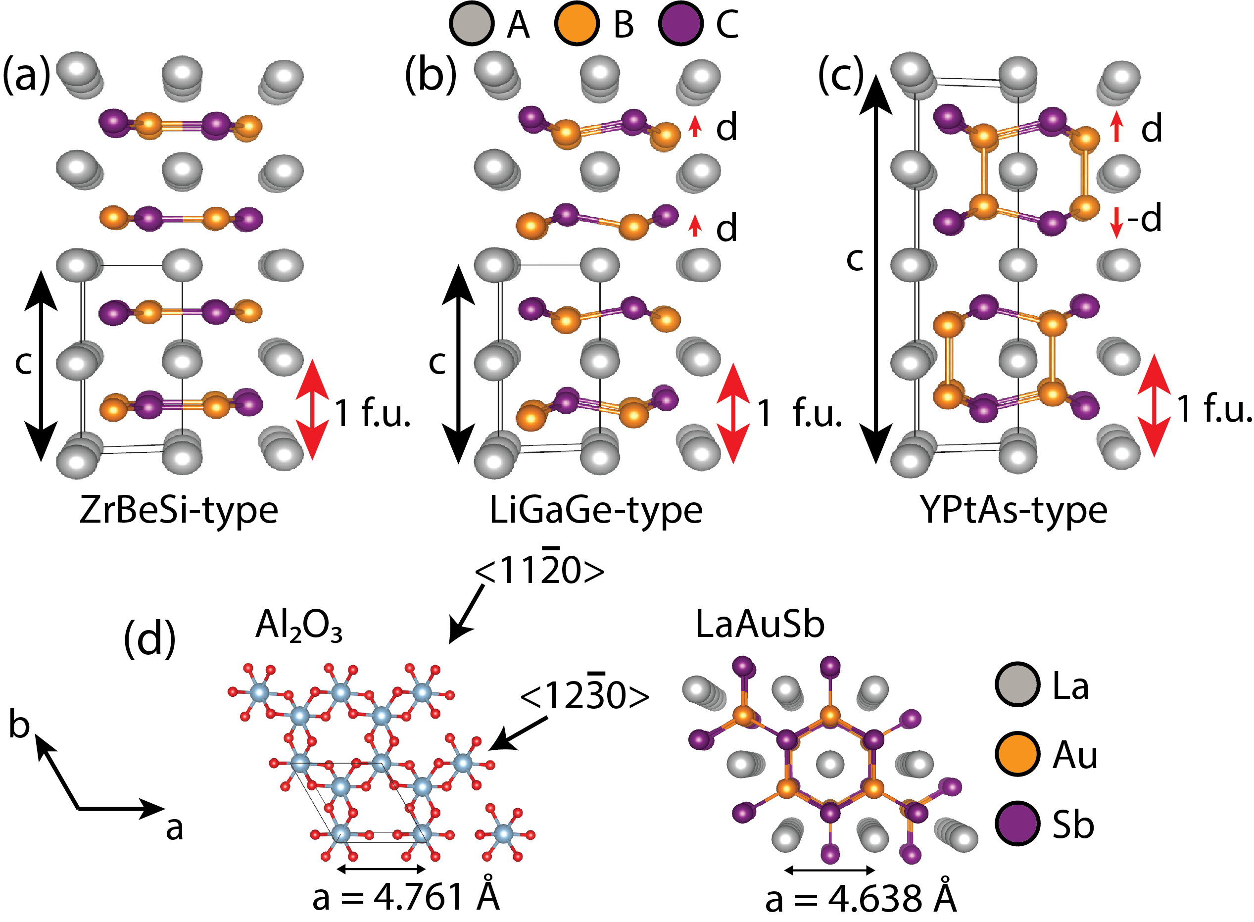
Valid PACS appear hereStructural distortions, especially layer buckling, are key to understanding and controlling the ferroic properties of hexagonal ternary intermetallics (composition ) Gao et al. (2018); Bennett et al. (2012); Narayan (2015). For example, consider the parent centrosymmetric ZrBeSi-type structure (space group ), which consists of planar graphitic layers that are “stuffed” with an spacer (Fig. 1(a)). Compounds with this structure are typically semimetals or Dirac semimetals, e.g., LaCuSn Casper et al. (2008) and BaAgBi Du et al. (2015). Upon decreasing the cation size via isovalent substitution, the planes typically buckle in a unidirectional pattern due to increased interlayer interactions, to yield the polar LiGaGe-type structure Bennett et al. (2012); Seibel et al. (2015) (space group , Fig. 1(b)). Here, the polar distortion gives rise to polar metallicity in the metallic state (e.g. LaAuGe, LaPtSb Du et al. (2018); Benedek and Birol (2016)) and predicted hyperferroelectricity in the insulating state (e.g. LiZnAs, NaZnSb), in which the long-range polarization is robust against the depolarizing field Bennett et al. (2012); Garrity et al. (2014). In such compounds the properties are determined by both the magnitude and the long-range ordering of the planar buckling, d, defined as the displacement along the axis between dissimilar atoms in the buckled plane Bennett et al. (2012). Due to this breaking of inversion symmetry, Weyl nodes are also predicted to exist in many LiGaGe-type s (e.g. KMgBi, LiZnBi) Di Sante et al. (2016); Gao et al. (2018); Cao et al. (2017). Tuning the magnitude and sign of buckling is proposed to change the crystal momenta and chirality of the Weyl nodes, or cause them to merge into a single Dirac point Gao et al. (2018). All of these predicted properties are defined by the buckling d in the system, therefore it is crucial to understand the origins of the buckling observed in these structures.
Recent experiments and theory suggest that in addition to cation size, the electron count may be an important handle for controlling the layer buckling. Whereas most stable s have 18 (or 8) valence electrons per formula unit corresponding to a filled (or ) configuration, the family AuSb ( lanthanide) has 19 valence electrons. The extra electron destabilizes the unidirectionally buckled LiGaGe-type structure, instead favoring a highly buckled structure with significant Au-Au interlayer bonding (Fig. 1c, YPtAs-type) Seibel et al. (2015). Importantly, although the resulting dimer buckled structure is centrosymmetric, the magnitude of buckling in the AuSb planes is predicted to be much larger than that observed in the LiGaGe-type polar structure Seibel et al. (2015). First principles calculations also suggested that LaAuSb hosts a Dirac cone within 100 meV of the Fermi energy Seibel et al. (2015). Therefore, an understanding of the coupling between electronic structure (electron count) and layer buckling in AuSb may be a path towards tuning the buckling, and hence ferroic properties, of LiGaGe-type compounds.
Here we use molecular beam epitaxy (MBE) to demonstrate the first epitaxial growth of LaAuSb. Our large area single crystalline films enable detailed structure and electronic property measurements and provide a path towards integration in layered heterostructures. The films are single crystalline and epitaxial to the -plane Al2O3 substrate, as measured by x-ray diffraction (XRD) and reflection high energy electron diffraction (RHEED). Scanning transmission electron microscopy (STEM) measurements reveal that the AuSb layer buckling is four times larger than the buckling in the 18-valence compounds LaPtSb and LaAuGe. Photoemission spectroscopy measurements of the valence bands are consistent with density functional theory calculations, and suggest that buckling results from an electronic instability that is suppressed in the buckled Au-Au dimer structure. Our results provide a route towards tuning the layer buckling and potential ferroic order in hexagonal s.
LaAuSb films were grown in a custom MBE system (MANTIS Deposition) on Al2O3 (0001) substrates (MTI) at a growth temperature of C as measured by pyrometer. The lattice mismatch between LaAuSb and Al2O3 is 3.2% tensile. Following the film growth, most samples were capped with amorphous Ge to prevent oxidation upon removal from the vacuum system. La and Au fluxes of atoms/cm2s were supplied from effusion cells, as measured by an in-situ quartz crystal monitor (QCM). Due to the high relative volatility of Sb, a 30% excess flux of Sb ( atoms/cm2s) was supplied using a cracker cell, similar to the strategy used for cubic Heusler compounds Patel et al. (2014); Kawasaki et al. (2014, 2018). Absolute fluxes were calibrated ex-situ by Rutherford Backscattering Spectrometry (RBS).
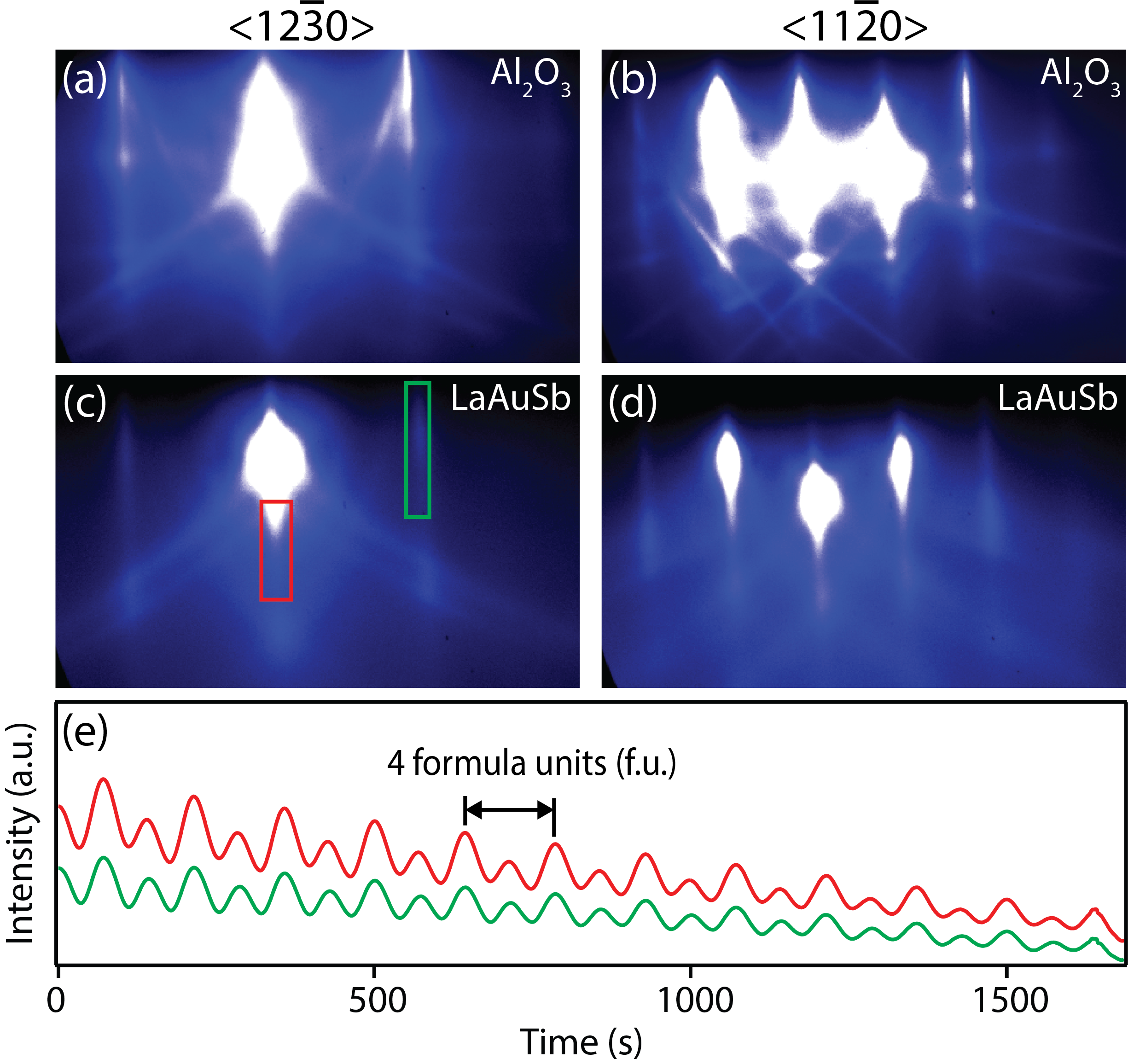
Figures 2a-d show typical RHEED patterns for the Al2O3 substrate and the LaAuSb film. The combination of sharp and streaky patterns and Kikuchi lines indicates the relatively smooth epitaxial growth with no apparent secondary phases. We observe persistent RHEED intensity oscillations throughout the entire growth, indicating a layer-by-layer growth mode. A representative example is shown in Fig. 2e, with a fundamental period of 70 s and a doubled beat period of 140 s. By comparison with the expected fluxes from QCM and RBS calibrations, this fundamental period of 70s corresponds to two formula units (f.u.) of LaAuSb (Fig. 1c).
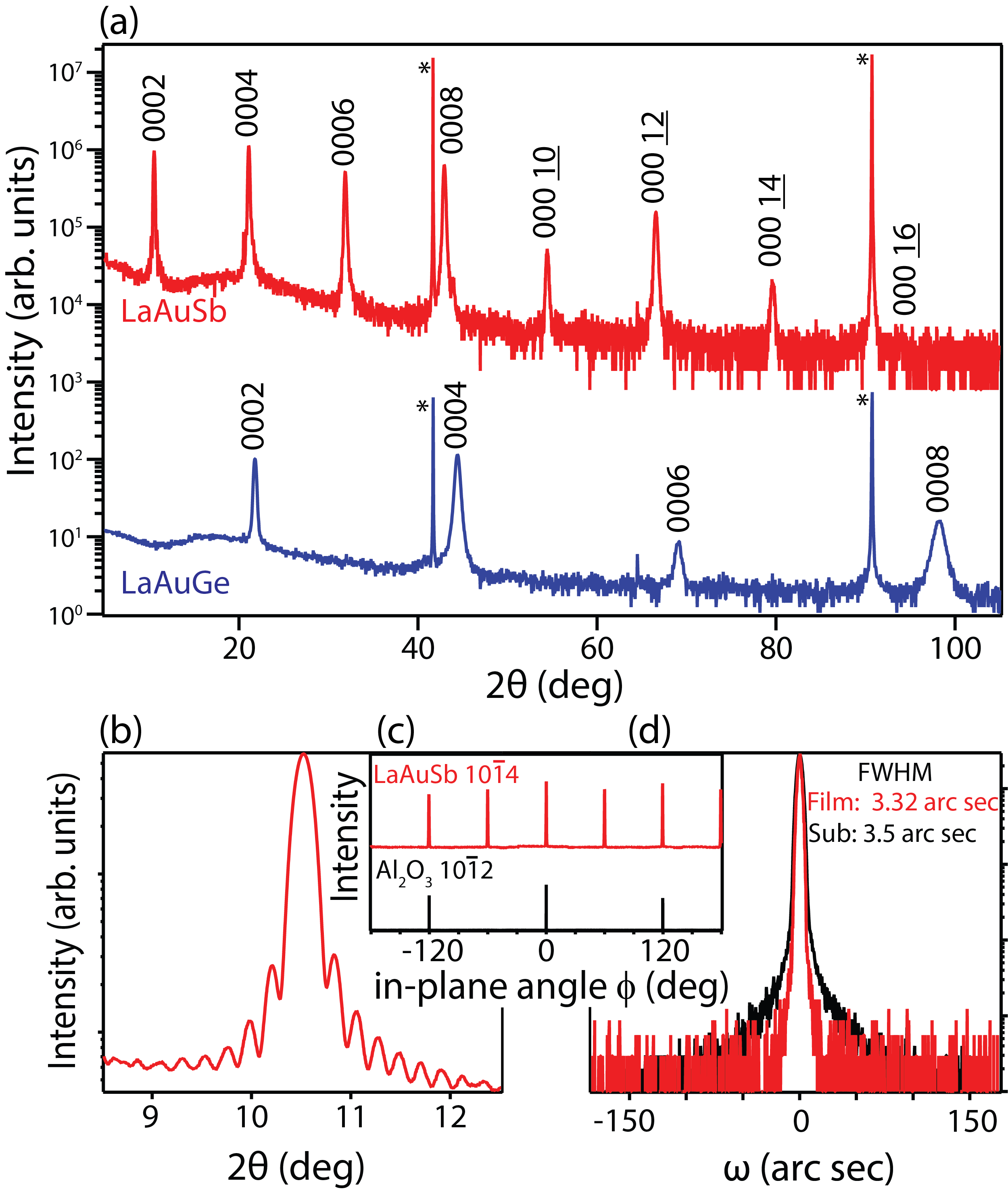
Phase purity and single-crystal quality were confirmed ex-situ by x-ray diffraction (XRD) using a Panalytical Empyrean diffractometer with Cu radiation. All scans used a quadruple-bounce Ge 220 monochromator on the incident beam. A second triple-bounce monochromator inserted in the diffracted beam path was inserted for the rocking curve measurements. Figure 3a shows the scan (red online) in which we observe only the expected sharp reflections and no secondary phases. For comparison we also plot a 2 scan of a LaAuGe film (blue online), which has 18 valence electrons and crystallizes in the undimerized LiGaGe-type structure Du et al. (2018). The presence of the 0002, 0006, 00010, and 00014 superstructure reflections in the LaAuSb confirms the doubling of the unit cell along the axis, consistent with Au-Au dimerization. For samples grown at temperatures below C, we do not observe the half-order superstructure reflections, suggesting a loss of long-range order. The superstructure-ordered sample grown at C displays sharp Kiessig fringes (Fig. 3b). The fringe spacing, averaged up to the fifth order, of 0.21 degrees corresponds to a film thickness of 41 nm, or 98 formula units, in good agreement with the 100 formula units expected from RHEED oscillations and QCM fluxes. Rocking curve widths for the film and substrate are sharp and approximately equal (3.32 and 3.5 arc seconds, respectively), indicating a high degree of in-plane ordering (Figure 3d). Pole figure measurements of the film 104 and substrate 102 reflections confirm the epitaxial relationship (Fig. 3c). From the pole figure and the measured out-of-plane lattice constant of Å, we extract an in-plane lattice constant of Å. This agrees well with the experimental powder diffraction lattice constants of Å and Å Seibel et al. (2015), indicating the 41 nm film on sapphire is nearly fully relaxed to the bulk lattice parameter.
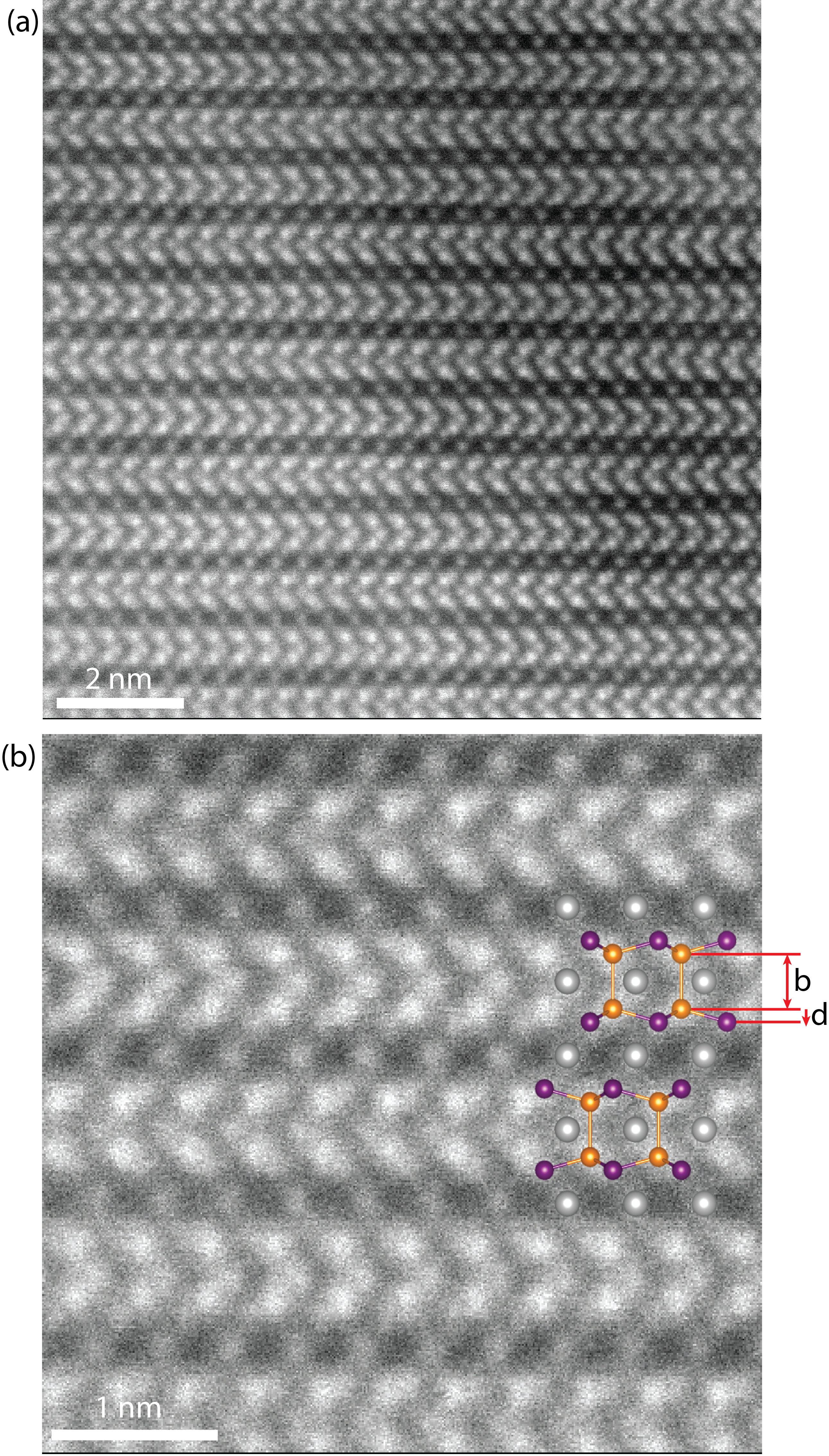
Scanning transmission electron microscopy (STEM) measurements confirm the Au-Au dimerized structure with a high degree of AuSb layer buckling. These measurements were performed using a FEI Titan STEM equipped with probe corrector using an operating voltage of 200 kV. High angle annular dark field (HAADF) STEM images were collected with a 24.5 mrad probe semi-convergence angle, 18.9 pA probe current, and HAADF detector range of 53.9-269.5 mrad. Annular bright field (ABF) images were collected simultaneously with an ABF detector range of 5.7-12.6 mrad. The sample was prepared for analysis using focused ion beam (FIB) milling. A FIB lamella was lifted out and attached to a Cu support grid prior to the final FIB milling to a thickness of nm. The final milling step was done using Ar ion milling using a Fischione Nanomill operated at 900 V, bringing the sample to a final thickness of nm before being transferred to the TEM column.
The high precision images seen in Figs. 4a and b were obtained by applying a non-rigid registration Yankovich et al. (2014) to the HAADF and ABF image series, respectively. Accurate positions of atomic sites were derived by fitting each peak on the HAADF image to a 2D Gaussian function. Sampling across 26 Au-Au pairs, we measure a Au-Au bond length of Å, which is in good agreement with the 3.12 Å expected from powder diffraction refinement Seibel et al. (2015). Averaging over 51 Au-Sb pairs, we find a planar buckling of Å also in good agreement with the 0.75 Å observed in bulk powder diffraction Seibel et al. (2015). This buckling is approximately four times larger than the bucklings observed in LiGaGe-type compounds with similar stoichiometry. In comparison, LaAuGe and LaPtSb have d of 0.180.01 Å and 0.220.01 Å, respectively Du et al. (2018).
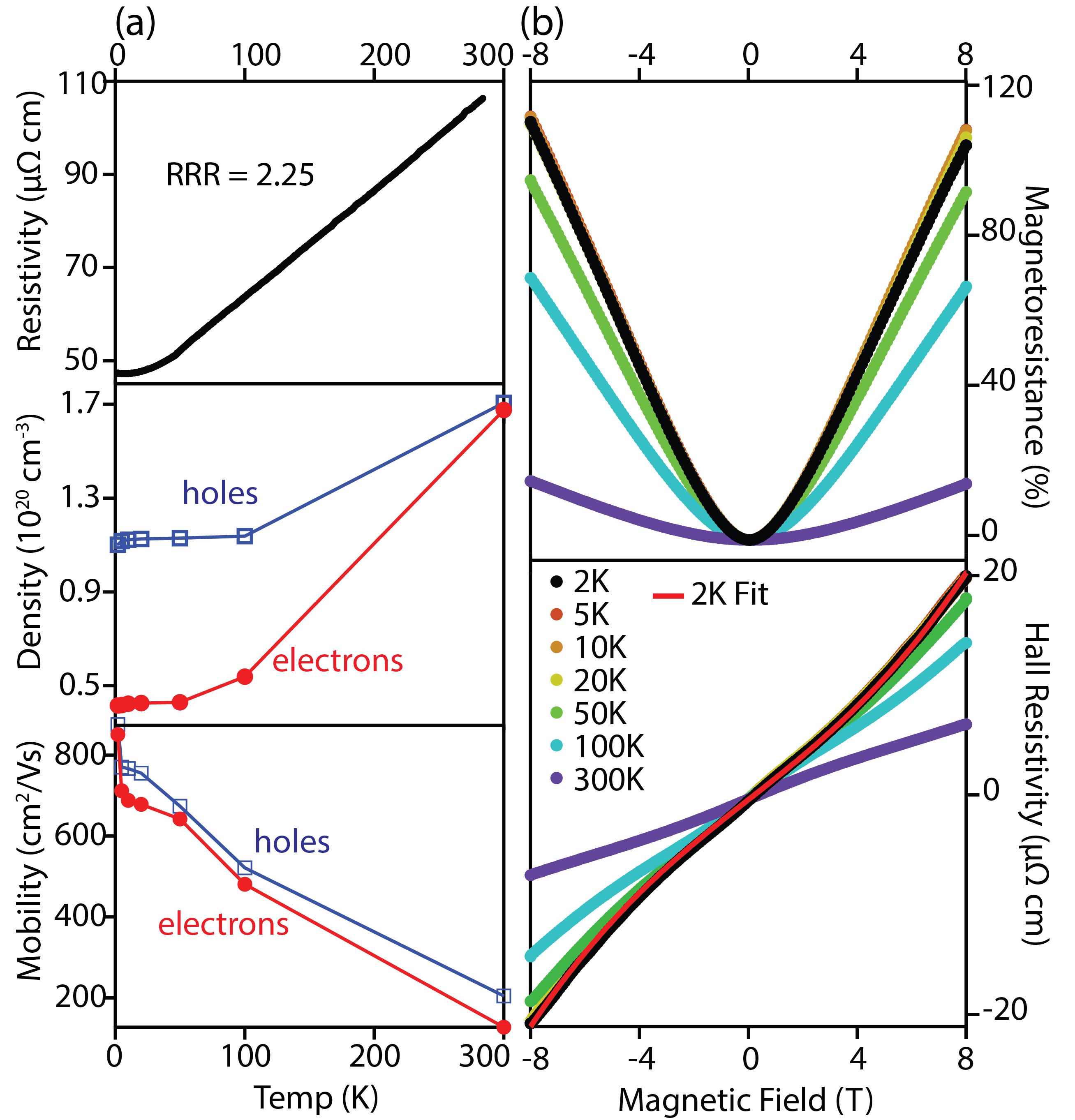
Magnetotransport properties were measured using a Quantum Design Physical Property Measurement System (PPMS). The resistivity versus temperature dependence at zero magnetic field shows strong metallic behavior with a residual resistivity ratio (RRR) of = 2.25 (Fig. 5a (top)). Longitudinal resistivity measurements as a function of out-of-plane magnetic field show magnetoresistance values of up to 109% at 2K at a field of 8T (Fig. 5b (top)). Hall effect measurements show a nonlinearity in vs B (Fig. 5b (bottom)), which we attribute to multiple carriers since LaAuSb is expected to be a semimetal. Therefore to extract the densities and mobilities we fit to a two-band model of the form Luo et al. (2015)
| (1) |
where () and () are the electron (hole) densities and mobilities, respectively. We first fit the slope of vs B in the range T to constrain the difference in carrier densities. We then adjust the concentrations and mobilities to fit (B) over the full field range, checking that that these parameters are also consistent with the zero-field resistivity .
A representative fit of at 2K is shown by the solid red curve in Fig. 5b (bottom). The extracted carrier densities and mobilities versus temperature are shown in Fig. 5a (middle) and (bottom), respectively. We find weakly varying electron and hole densities of order cm-3, consistent with expectations for a semimetal, and mobilities approaching 1000 cm2/Vs in the low temperature limit (2K).
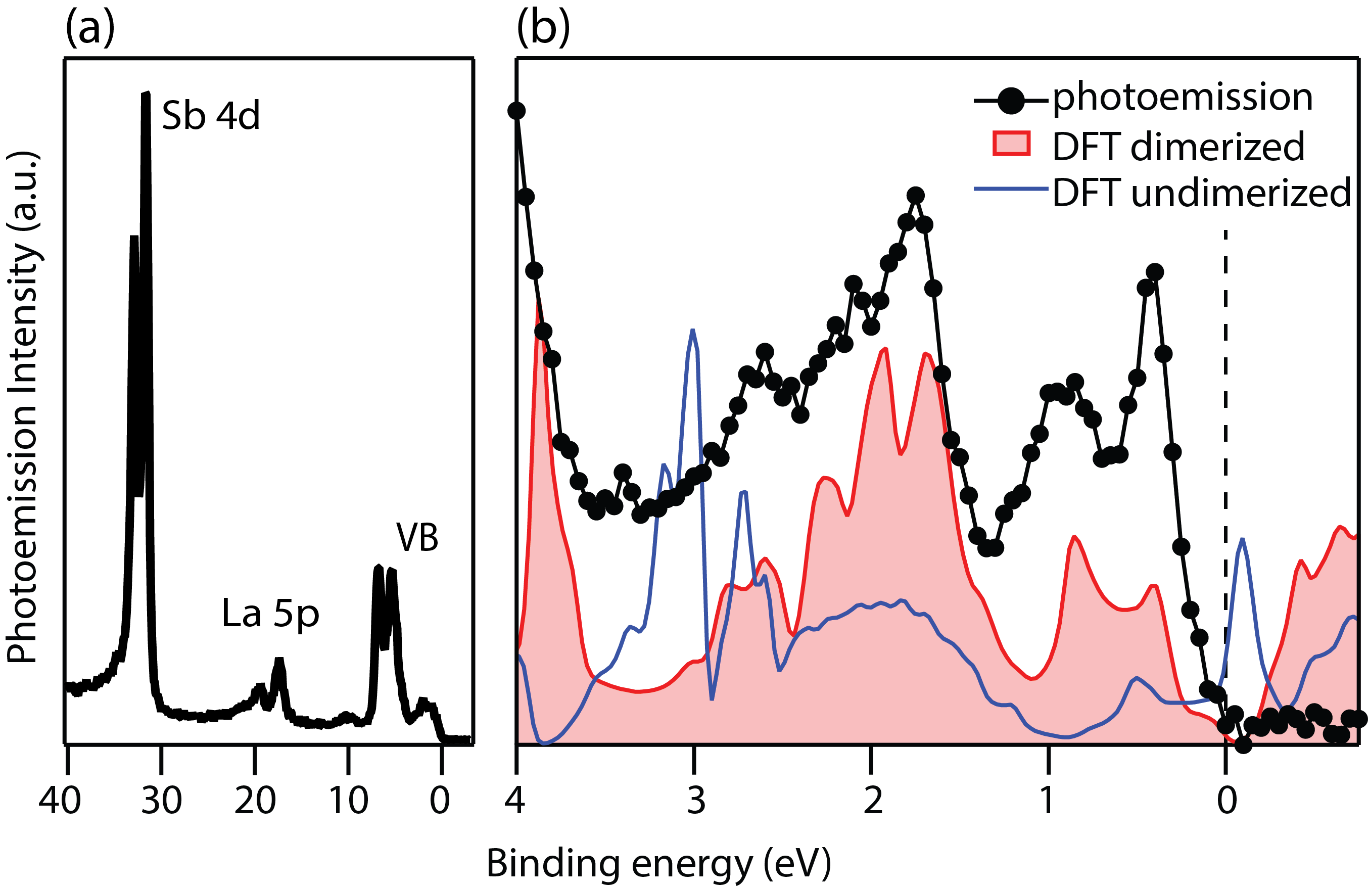
To investigate the origins of the Au dimer buckling and its relation to electronic structure, photoemission spectroscopy measurements were performed at beamline 29-ID of the of the Advanced Photon Source (APS), using a Scienta R4000 analyzer (angular acceptance angle of 14 degrees) and incident photon energies in the range 300 to 2000 eV (Fig. 6). The Fermi level was referenced measurements of a gold screw that is in electrical contact with the sample. To protect the surfaces, these samples were transported to the APS using an ultrahigh vacuum suitcase (pressure less than Torr, no Ge cap). For comparison with experiment, density functional theory calculations were performed using the Perdew - Becke - Ernzerhof (PBE) parametrization of the generalized gradient approximation including fully relativistic spin-orbit coupling effects (GGA+SO), as implemented in WIEN2k Blaha et al. (2018). Further details about the calculation parameters are found in Seibel et al. (2015). For the dimerized structure we used the bulk atomic positions as reported in Ref. Seibel et al. (2015). The calculated electronic structure is also consistent with Ref. Seibel et al. (2015).
We observe good qualitative agreement between the measured angle-integrated valence band spectrum (Fig. 6, black symbols) and GGA+SO calculation for the dimerized structure (Fig. 6b, shaded red curve). The measured valence band width is approximately 1 eV and decreases to a sharp but finite minimum at the Fermi energy, consistent with the behavior expected for a semimetal or Dirac semimetal Seibel et al. (2015).
We also compare the photoemission measurement to a GGA+SO calculation for LaAuSb in a hypothetical undimerized LiGaGe-type structure (Fig. 1b). For this hypothetical structure we fix the in-plane lattice constant and the out-of-plane functional unit spacing to that of the dimerized YPtAs-type structure, and apply the same buckling d but in a uniform direction with layer stacking sequence. We find that this structure exhibits a sharp peak in the density of states just above the Fermi energy, which is expected to be unstable (Fig. 6b, blue curve). In comparison, for the dimerized structure there is a strong suppression in the density of states resulting in a pseudo-gap at the Fermi energy. Our measurements and comparisons with theory suggest an electronic origin for the dimerization, akin to a Peierls distortion, and consistent with the formal electron count of La (Au-Au)0 Sb suggested previously by first-principles calculations Seibel et al. (2015). In this picture, the Au-Au dimerization is responsible for suppressing the density of states at .
In summary, we demonstrated the epitaxial single-crystalline growth of the 19 valence electron compound LaAuSb. Due to the strong electronic driving force for Au-Au dimerization, the resultant AuSb layer buckling is four times larger than the buckling observed in 18-electron s. Our epitaxial films exhibit relatively large mobility and magnetoresistance with carrier concentrations consistent with that of a compensated semi-metal. Lastly, we showed that our measured valence band structure is consistent with the proposed dimerized electronic structure, providing strong evidence for an electronic driving force towards Au-Au dimerization, and therefore buckling, in these 19 valence electron count compounds.
Acknowledgments. This work was supported primarily by the United States Army Research Office (ARO Award number W911NF-17-1-0254). Travel for photoemission spectroscopy measurements was supported by the CAREER program of the National Science Foundation (DMR-1752797). This research used resources of the Advanced Photon Source, a U.S. Department of Energy (DOE) Office of Science User Facility operated for the DOE Office of Science by Argonne National Laboratory under Contract No. DE-AC02-06CH11357; additional support by National Science Foundation under Grant no. DMR-0703406. We gratefully acknowledge the use of x-ray diffraction facilities supported by the NSF through the University of Wisconsin Materials Research Science and Engineering Center under Grant No. DMR-1720415. We thank Professor Song Jin for the use of PPMS facilities. We thank Mark Mangus (Eyring Materials Center, Arizona State University) and Greg Haugstad (Characterization Facility, University of Minnesota) for performing RBS measurements.
References
- Gao et al. (2018) H. Gao, Y. Kim, J. W. F. Venderbos, C. L. Kane, E. J. Mele, A. M. Rappe, and W. Ren, Phys. Rev. Lett. 121, 106404 (2018), URL https://link.aps.org/doi/10.1103/PhysRevLett.121.106404.
- Bennett et al. (2012) J. W. Bennett, K. F. Garrity, K. M. Rabe, and D. Vanderbilt, Physical review letters 109, 167602 (2012).
- Narayan (2015) A. Narayan, Phys. Rev. B 92, 220101(R) (2015), URL https://journals.aps.org/prb/abstract/10.1103/PhysRevB.92.220101.
- Casper et al. (2008) F. Casper, C. Felser, R. Seshadri, C. Sebastian, and R. Pöttgen, J. Phys. D: Appl. Phys. 41, 035002 (2008), URL stacks.iop.org/JPhysD/41/035002.
- Du et al. (2015) Y. Du, B. Wan, D. Wang, L. Sheng, C.-G. Duan, and X. Wan, Scientific Reports 5 (2015), URL https://www.nature.com/articles/srep14423.
- Seibel et al. (2015) E. M. Seibel, L. M. Schoop, W. Xie, Q. D. Gibson, J. B. Webb, M. K. Fuccillo, J. W. Krizan, and R. J. Cava, J. Am. Chem. Soc. 137, 1282 (2015).
- Du et al. (2018) D. Du, P. Strohbeen, E. Shourov, C. Zhang, P. Voyles, and J. Kawasaki, Un-published (2018).
- Benedek and Birol (2016) N. A. Benedek and T. Birol, Journal of Materials Chemistry C 4, 4000 (2016).
- Garrity et al. (2014) K. F. Garrity, K. M. Rabe, and D. Vanderbilt, Phys. Rev. Lett. 112, 127601 (2014), URL https://link.aps.org/doi/10.1103/PhysRevLett.112.127601.
- Di Sante et al. (2016) D. Di Sante, P. Barone, A. Stroppa, K. F. Garrity, D. Vanderbilt, and S. Picozzi, Phys. Rev. Lett. 117, 076401 (2016), URL https://link.aps.org/doi/10.1103/PhysRevLett.117.076401.
- Cao et al. (2017) W. Cao, P. Tang, Y. Xu, J. Wu, B.-L. Gu, and W. Duan, Phys. Rev. B 96, 115203 (2017), URL https://journals.aps.org/prb/pdf/10.1103/PhysRevB.96.115203.
- Momma and Izumi (2011) K. Momma and F. Izumi, J. Appl. Crystallogr. 44, 1272 (2011).
- Patel et al. (2014) S. J. Patel, J. K. Kawasaki, J. Logan, B. D. Schultz, J. Adell, B. Thiagarajan, A. Mikkelsen, and C. J. Palmstrøm, Applied Physics Letters 104, 201603 (2014).
- Kawasaki et al. (2014) J. K. Kawasaki, L. I. Johansson, B. D. Schultz, and C. J. Palmstrøm, Applied Physics Letters 104, 022109 (2014).
- Kawasaki et al. (2018) J. K. Kawasaki, A. Sharan, L. I. Johansson, M. Hjort, R. Timm, B. Thiagarajan, B. D. Schultz, A. Mikkelsen, A. Janotti, and C. J. Palmstrøm, Science advances 4, eaar5832 (2018).
- Yankovich et al. (2014) A. B. Yankovich, B. Berkels, W. Dahmen, P. Binev, S. Sanchez, A. Bradley, S.A. Li, I. Szlufarska, and P. M. Voyles, Nature Communications 5 (2014).
- Luo et al. (2015) Y. Luo, H. Li, Y. Dai, H. Miao, Y. Shi, H. Ding, A. Taylor, D. Yarotski, R. Prasankumar, and J. Thompson, Appl. Phys. Lett. 107 (2015).
- Blaha et al. (2018) P. Blaha, K. Schwarz, G. Madsen, D. Kvasnicka, J. Luitz, R. Laskowski, F. Tran, and L. Marks (2018).