Focused ion beam modification of non-local magnon-based transport in yttrium iron garnet/platinum heterostructures
Abstract
We study the impact of \chGa ion exposure on the local and non-local magnetotransport response in heterostructures of the ferrimagnetic insulator yttrium iron garnet and platinum. In particular, we cut the yttrium iron garnet layer in between two electrically separated wires of platinum using a \chGa ion beam, and study the ensuing changes in the magnetoresistive response. We find that the non-local magnetoresistance signal vanishes when the yttrium iron garnet film between the Pt wires is fully cut, although the local spin Hall magnetoresistance signal remains finite. This observation corroborates the notion that pure spin currents carried by magnons are crucial for the non-local magnetotransport effects observed in magnetic insulator/metal nanostructures.
Pure spin transport phenomena give access to important magnetic and magnonic properties of magnetic insulators.Althammer et al. (2013); Nakayama et al. (2013); Chen et al. (2013); Aqeel et al. (2015); Cornelissen et al. (2015); Goennenwein et al. (2015); Ganzhorn et al. (2016a); Hoogeboom et al. (2017) Taking advantage of the spin Hall effect and the inverse spin Hall effect, pure spin currents can be driven into and detected across the interface between a spin Hall active metal and a magnetic insulator.Hirsch (1999); Chen et al. (2013); Althammer et al. (2013); Zhang and Zhang (2012a, b) In particular, the spin Hall magnetoresistance (SMR) allows to probe the magnetic sublattice structure of the magnetic insulator.Althammer et al. (2013); Nakayama et al. (2013); Chen et al. (2013); Aqeel et al. (2015); Ganzhorn et al. (2016a); Hoogeboom et al. (2017) In addition, non-local experiments in nanoscale structures with several electrically separated metal wires allow to experimentally access the magnon diffusion length in the magnetic insulator.Zhang and Zhang (2012a, b); Cornelissen et al. (2015); Goennenwein et al. (2015); Bender and Tserkovnyak (2015) This non-local approach thus enables studies of the properties of magnetic excitations and their diffusion in the ferromagnetic insulator, and holds the potential for faster and more energy-efficient data processing applications.Chumak, Serga, and Hillebrands (2014); Ganzhorn et al. (2016b)
While the non-local transport experiments in magnetic insulator/metal heterostructures so far were discussed and modeled in terms of magnon diffusion, a smoking gun proof that magnons indeed are the relevant transport quantum has not been put forward. Moreover, speculations about different mechanisms surfaced recently, suggesting that angular momentum can also be carried by phonons, that couple the lattice to the magnetic system.Streib, Keshtgar, and Bauer (2018)
Additionally, the observation of non-local transport signatures in Pt wires on a paramagnetic substrate cast doubt on the importance of magnons.Oyanagi et al. (2018) Furthermore, higher order effects attributed to magnon swasing and condensation have been observed.Wimmer et al. (2018); Thiery et al. (2018); Cornelissen et al. (2018); Bender et al. (2014) In order to ascertain that magnetic excitations indeed are essential for non-local magnetotransport in magnetic insulator/metal heterostructures, it thus appears mandatory to perform a “scratch test”, i.e. , to remove the magnetic material in between the metal wires (cf. Fig. 1a)).
In this letter we use a focused ion beam (FIB) of \chGa ions to alter and remove the yttrium iron garnet (YIG) in between two platinum wires nanopatterned onto the YIG surface. By performing this nano-scale scratch test, we verify that the non-local effects indeed are suppressed when the YIG is removed. Our findings thus corroborate the notion that magnon diffusion is key for the non-local magnetotransport in magnetic insulator/metal heterostructures.
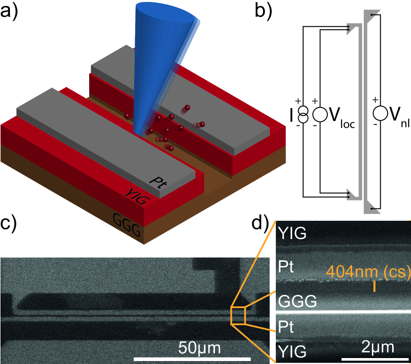
The samples were prepared starting from commercially available, thick YIG (\chY3Fe5O12) films deposited on (111)-oriented \chGd3Ga5O12 (GGG) substrates via liquid phase epitaxy. Prior to the platinum deposition, the samples were first cleaned using a Piranha solution (\chH2SO4:H2O2 in a ratio of 1:1 by volume) to remove organic constituents from the YIG surface. They were then annealed at for in vacuum in the sputtering chamber, before a thick platinum film was sputter deposited. The Pt films were subsequently patterned via optical lithography and \chAr^+ ion milling. The typical distance between our platinum wires is and their length and width is and , respectively.
To obtain the local and non-local magnetoresistive response, we use a Keithley 2450 sourcemeter to drive a DC current of along one platinum wire, referred to as the left wire for simplicity in the following. The local and non-local voltage drop is simultaneously detected by two Keithley 2182 nanovoltmeters on the left and right wire, respectively (cf. Fig. 1b)). To increase the measurement sensitivity and to allow the separation of effects related to electric and thermal magnon generation, we employ a current reversal technique:Goennenwein et al. (2015)
| (1) |
In particular, this antisymmetrization allows to investigate only the resistive response (as opposed to the thermal response observed in the symmetric signal).Avci et al. (2015); Schreier et al. (2013) A magnetic field is applied using a cylindrical Halbach arrayHalbach (1980). By rotating this diametrically magnetized Halbach array (the angle of rotation is denoted as ), we can measure the magnetotransport response as a function of the magnetic field orientation.
The FIB patterning and the scanning ion and electron microscopy experiments were conducted in a FEI Helios NanoLab DualBeam system. The aperture for the \chGa FIB was set to and the acceleration voltage was . A scanning ion image of a typical structure prior to cutting and an electron microscopy image depicting the structure after FIB patterning are shown in Fig. 1c) and d), respectively.
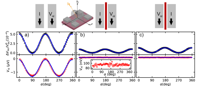
We will now turn to the discussion of the transport signatures. Prior to FIB milling, the local and non-local transport was characterized. The resulting local and non-local signal and are shown in Fig. 2a). We obtain the magnetoresistance (MR) from the raw data by using
| (2) |
This MR exhibits a modulation and was verified to show the signature of the spin Hall magnetoresistance (SMR) from rotations in three mutually orthogonal rotation planes. For further details on the fingerprint of the SMR, please refer to refs. Althammer et al. (2013); Goennenwein et al. (2015). The effect magnitude (i.e. the amplitude of the modulation) is within the typical range of values reported for YIG/Pt bilayers with of Pt deposited ex-situ via sputtering.Pütter et al. (2017); Schlitz et al. (2018)
The non-local signal also shows a modulation with an amplitude of and no offset. This is the behavior expected for the magnon mediated magnetoresistance (MMR).Goennenwein et al. (2015); Cornelissen et al. (2015) Please note, that the non-local voltage shown in Fig. 2a) has only been antisymmetrized (cf. Eq. (1)), no offset has been subtracted.
After FIB-cutting the YIG film in between the two platinum wires, removing a square with an area of and a width of to a depth of , the magnetotransport response changes significantly (cf. Fig. 2b)). While the SMR decreases by a factor of 5 to , the MMR (i.e. the modulation of the non-local voltage with magnetic field orientation) vanishes to within the experimental resolution () and thus is reduced by at least a factor 200. Please note, that the slight positive offset of is most likely a result of a cross conductivity between the two Pt strips caused by \chGa ion implantation. Assuming that the (anisotropic) magnetoresistance visible in the conductive channel is , the cross conduction will lead to a maximum modulation of , well below our resolution limit.
The absence of a non-local magnetotransport signal could be naturally explained if the right (“non-local”) Pt wire would have been destroyed or made spin Hall inactive by the FIB process. We therefore repeated the magnetotransport experiments now using the right wire as the “local” wire, and detecting the non-local voltage on the left wire (cf. Fig. 2c)). The resulting measurements show the same salient features, i.e. a clear local SMR also on the right Pt strip, along with a complete absence of the MMR. Again, the local SMR amplitude is reduced as compared to the measurement taken before the FIB cut. This demonstrates that both Pt wires still are spin Hall active, with a clear local SMR response. Since, the local SMR and the non-local MMR depend on electrically generated and detected spin transport, they both are sensitive to the square of the spin Hall angle. Thus, a reduction of the spin Hall angle of the platinum films due to the FIB process can not account for the vanishing non-local effect.Cornelissen et al. (2015); Zhang and Zhang (2012a, b); Chen et al. (2013); Althammer et al. (2013) These findings suggest that magnon transport indeed is mandatory for a finite MMR. The FIB cut removes the magnetic material in between the Pt wires and thus removes the magnetic medium mandatory for magnon transport.
Apart from magnon diffusion, another mechanism to consider for a finite non-local signal is the transport of the angular momentum by phonons. Since phonons can propagate in particular also in the substrate and not only in the YIG film, this transport channel for the non-local voltage generation should remain open even after FIB patterning of the YIG. Please note, that we do increase the diffusion distance when removing material in between the platinum wires: Upon removal of a square cross section with a width of and a depth of roughly , the effective diffusion distance is increased approximately by a factor of 2 (i.e. from 1 to ). Assuming a diffusion length of to and one dimensional diffusion, the signal would be reduced by a factor of or , respectively.Cornelissen et al. (2015); Goennenwein et al. (2015) This cannot explain our findings, even if we include the reduction of the local signal by a factor of 5. Therefore, we conclude that indeed magnons must be the transport quantum relevant for the non-local magnetotransport effect.
To further elucidate the involved mechanisms, we used a second device and performed a cut over only half the length of the platinum wire. The resulting non-local magnetoresistance measurements before and after cutting are shown in Fig. 3a) and b), respectively. In a simple picture, one would expect that the removal of half of the YIG in between the platinum wires would lead to a factor of 2 reduction of the non-local signal. In our experiment, however, the MMR is decreased by roughly a factor of three. Please note, that for this device, in contrast to the reduction to 0.2 of the initial value for the full cut device, here, the SMR is only decreased to 0.6 of the value prior to cutting.
We speculate, that either the YIG/Pt interface or the layers themselves are modified already by imaging of the device with the scanning ion beam, explaining the reduction of the magnetotransport response beyond the factor of 2 expected from the geometrical changes (YIG cut half-length). Since the penetration depth of the \chGa ions at the given acceleration voltage is in the range of , this assumption is reasonable.Moll (2018) However, more systematic \chGa ion beam irradiation experiments will be required in the future to clarify this point. Regarding the non-local signal the experimentally observed reduction of the MMR by a factor of three can be straightforwardly rationalized as follows: Considering, that half of the device can not contribute (no YIG film in between the Pt strips), the non-local signal in the functioning half of the device is decreased to roughly 0.7 of the inital amplitude upon irradiation. We thus must conclude that the ion irradiation alone cannot be sufficient to explain the absence of the non-local magnetotransport signal in the first device (cf. Fig. 2).
Finally, to also study the impact of the increased \chGa ion irradiation between the platinum wires, we investigated a third device, where the FIB cut was performed over the full length of the device but with a lower depth of 50-, i.e. less than half of the YIG thickness. The corresponding non-local magnetoresistance curves prior and after cutting are shown in Fig. 3c) and d).
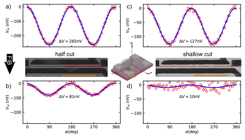
We will now try to extrapolate the non-local magnetrotransport signal based on our previous observations: We expect that the signal is decreased to about 0.7 of its initial value just because of the imaging of the device with the \chGa ions. Additionally, we have removed roughly half of the YIG layer (thickness) in the channel with the FIB. Thus, the signal should be reduced to roughly , which is approximately four times larger than the signal observed in the experiment (cf. Fig. 3d)). We therefore conclude that either \chGa ion implantation is very efficient in altering the magnonic properties of the YIG film or the constriction of the transport channel leads to additional boundary conditions for the magnon transport.Chumak, Serga, and Hillebrands (2017) This can be potentially useful in the creation of magnonic crystals necessary for single mode magnon transport, where periodic alterations of the YIG properties are crucial.Chumak, Serga, and Hillebrands (2017) Please note, that also for the shallow cut, the SMR is reduced only to 0.6 of its initial value, compared to 0.2 for the deep cut.
In conclusion, we have found that FIB patterning of the YIG film in between the two platinum wires very sensitively affects the local and non-local magnetotransport response of YIG/Pt heterostructures. Our results corroborate the notion that magnon diffusive transport is key for the observed non-local magnetotransport signatures in these nanostructures. Additionally, by studying the impact of FIB cuts to different depths and with different lengths, we conclude that YIG/Pt devices are very sensitive to \chGa ion irradiation. This opens new avenues for (periodic) modulation of the magnonic/magnetic properties of such devices.
We thank T. Schönherr and S. Piontek for technical support. We acknowledge financial support by the Deutsche Forschungsgemeinschaft via SPP 1538 (project no. GO 944/4).
References
- Althammer et al. (2013) M. Althammer, S. Meyer, H. Nakayama, M. Schreier, S. Altmannshofer, M. Weiler, H. Huebl, S. Geprägs, M. Opel, R. Gross, D. Meier, C. Klewe, T. Kuschel, J.-M. Schmalhorst, G. Reiss, L. Shen, A. Gupta, Y.-T. Chen, G. E. W. Bauer, E. Saitoh, and S. T. B. Goennenwein, Physical Review B 87, 224401 (2013).
- Nakayama et al. (2013) H. Nakayama, M. Althammer, Y.-T. Chen, K. Uchida, Y. Kajiwara, D. Kikuchi, T. Ohtani, S. Geprägs, M. Opel, S. Takahashi, R. Gross, G. E. W. Bauer, S. T. B. Goennenwein, and E. Saitoh, Physical Review Letters 110, 206601 (2013).
- Chen et al. (2013) Y.-T. Chen, S. Takahashi, H. Nakayama, M. Althammer, S. T. B. Goennenwein, E. Saitoh, and G. E. W. Bauer, Physical Review B 87, 144411 (2013).
- Aqeel et al. (2015) A. Aqeel, N. Vlietstra, J. A. Heuver, G. E. W. Bauer, B. Noheda, B. J. van Wees, and T. T. M. Palstra, Physical Review B 92, 224410 (2015).
- Cornelissen et al. (2015) L. J. Cornelissen, J. Liu, R. A. Duine, J. B. Youssef, and B. J. van Wees, Nature Physics 11, 1022 EP (2015).
- Goennenwein et al. (2015) S. T. B. Goennenwein, R. Schlitz, M. Pernpeintner, K. Ganzhorn, M. Althammer, R. Gross, and H. Huebl, Applied Physics Letters 107, 172405 (2015).
- Ganzhorn et al. (2016a) K. Ganzhorn, J. Barker, R. Schlitz, B. A. Piot, K. Ollefs, F. Guillou, F. Wilhelm, A. Rogalev, M. Opel, M. Althammer, S. Geprägs, H. Huebl, R. Gross, G. E. W. Bauer, and S. T. B. Goennenwein, Physical Review B 94, 094401 (2016a).
- Hoogeboom et al. (2017) G. R. Hoogeboom, A. Aqeel, T. Kuschel, T. T. M. Palstra, and B. J. van Wees, Applied Physics Letters 111, 052409 (2017).
- Hirsch (1999) J. E. Hirsch, Physical Review Letters 83, 1834 (1999).
- Zhang and Zhang (2012a) S. S.-L. Zhang and S. Zhang, Physical Review Letters 109, 096603 (2012a).
- Zhang and Zhang (2012b) S. S.-L. Zhang and S. Zhang, Physical Review B 86, 214424 (2012b).
- Bender and Tserkovnyak (2015) S. A. Bender and Y. Tserkovnyak, Physical Review B 91, 140402 (2015).
- Chumak, Serga, and Hillebrands (2014) A. V. Chumak, A. A. Serga, and B. Hillebrands, Nature Communications 5 (2014).
- Ganzhorn et al. (2016b) K. Ganzhorn, S. Klingler, T. Wimmer, S. Geprägs, R. Gross, H. Huebl, and S. T. B. Goennenwein, Applied Physics Letters 109, 022405 (2016b).
- Streib, Keshtgar, and Bauer (2018) S. Streib, H. Keshtgar, and G. E. W. Bauer, Physical Review Letters 121, 027202 (2018).
- Oyanagi et al. (2018) K. Oyanagi, S. Takahashi, L. J. Cornelissen, J. Shan, S. Daimon, T. Kikkawa, G. E. W. Bauer, B. J. van Wees, and E. Saitoh, arXiv e-prints:1811.11972 (2018).
- Wimmer et al. (2018) T. Wimmer, M. Althammer, L. Liensberger, N. Vlietstra, S. Geprägs, M. Weiler, R. Gross, and H. Huebl, arXiv e-prints:1812.01334 (2018).
- Thiery et al. (2018) N. Thiery, A. Draveny, V. V. Naletov, L. Vila, J. P. Attané, C. Beigné, G. de Loubens, M. Viret, N. Beaulieu, J. Ben Youssef, V. E. Demidov, S. O. Demokritov, A. N. Slavin, V. S. Tiberkevich, A. Anane, P. Bortolotti, V. Cros, and O. Klein, Physical Review B 97, 060409 (2018).
- Cornelissen et al. (2018) L. J. Cornelissen, J. Liu, B. J. van Wees, and R. A. Duine, Physical Review Letters 120, 097702 (2018).
- Bender et al. (2014) S. A. Bender, R. A. Duine, A. Brataas, and Y. Tserkovnyak, Physcial Review B 90, 094409 (2014).
- Avci et al. (2015) C. O. Avci, K. Garello, A. Ghosh, M. Gabureac, S. F. Alvarado, and P. Gambardella, Nature Physics 11, 570 EP (2015), article.
- Schreier et al. (2013) M. Schreier, A. Kamra, M. Weiler, J. Xiao, G. E. W. Bauer, R. Gross, and S. T. B. Goennenwein, Physical Review B 88, 094410 (2013).
- Halbach (1980) K. Halbach, Nuclear Instruments and Methods 169, 1 (1980).
- Pütter et al. (2017) S. Pütter, S. Geprägs, R. Schlitz, M. Althammer, A. Erb, R. Gross, and S. T. B. Goennenwein, Applied Physics Letters 110, 012403 (2017).
- Schlitz et al. (2018) R. Schlitz, A. A. Amusan, M. Lammel, S. Schlicht, T. Tynell, J. Bachmann, G. Woltersdorf, K. Nielsch, S. T. B. Goennenwein, and A. Thomas, Applied Physics Letters 112, 242403 (2018).
- Moll (2018) P. J. Moll, Annual Review of Condensed Matter Physics 9, 147 (2018).
- Chumak, Serga, and Hillebrands (2017) A. V. Chumak, A. A. Serga, and B. Hillebrands, Journal of Physics D: Applied Physics 50, 244001 (2017).